Pr. Jaume Esteve (CNM-IMB CSIC) Dr. María Aránzazu Uranga ... · participate in the EPSON’s...
241
Transcript of Pr. Jaume Esteve (CNM-IMB CSIC) Dr. María Aránzazu Uranga ... · participate in the EPSON’s...


Directors: Pr. Jaume Esteve (CNM-IMB CSIC) Dr. María Aránzazu Uranga (UAB) Dr. Pascal Nouet (LIRMM – UMR: CNRS-UM2) El professor Jaume Esteve, Professor d’Investigació del Consell Superior d’Investigacions Científiques (CSIC) al Institut de Microelectrònica de Barcelona del Centre Nacional de Microelectrònica (CNM-IMB), la doctora María Aránzazu Uranga, professora agregada del departament de Enginyeria Electrònica de la Universitat Autònoma de Barcelona a Bellaterra, i el doctor Pascal Nouet, professor a la Université Montpellier II i investigador del Laboratoire d’Informatique de Robotique et de Microélectronique de Montpellier (LIRMM), unitat mixta de recerca del Centre Nacional d’Investigacions Científiques (CNRS) i de la Université Montpellier II, CERTIFIQUEN que la present memòria titulada ‘Thin-film bulk acoustic wave resonators (FBAR): fabrication, heterogeneous integration with CMOS technologies and sensor applications’ ha estat realitzada sota la seva direcció per en Humberto Campanella Pineda Bellaterra i Montpellier, desembre 2007

Aura matutinae: nivea et bianchissima Alba del Aire, Mar, Río...
“Por eso Rafael Santos yo quiero dejarte dicho en esta canción que si te inspira ser zapatero sólo quiero que seas el mejor pues de nada sirve el doctor
si es el ejemplo malo del pueblo”
Mi muchacho, Diomedes Díaz

Thin-film bulk acoustic wave resonators – FBAR: Fabrication, heterogeneous integration with CMOS technologies and
sensor applications
Humberto Campanella
Submitted in partial fulfillment of the requirements for obtaining the Ph.D. degrees at both Université de Montpellier II (UM2) and Universitat Autònoma de Barcelona (UAB)
Abstract
The high impact of FBAR on radio-frequency and, most recently, on sensing systems has motivated the development of integrated applications. This means that the fabrication process should succeed in producing high-quality-factor resonators and, at the same time, in integrating FBARs with standard CMOS technologies. Hence, this Ph.D. thesis addresses these requirements by contributing with the design, fabrication and characterization of thin-film bulk acoustic wave resonators (FBAR); their integration with standard complementary-metal-oxide-semiconductor (CMOS) technologies; and their application to sensing systems.
The development of the FBAR’s fabrication technology has involved the set up of the deposition and micro-machining techniques of the layered structure of the resonator, which comprises an acoustic layer made of aluminum nitride (AlN). Several tests on the deposition and characterization of the AlN quality were carried out. Also, different micro-machining technologies for FBAR releasing were tested, the front-side micro-machining technique having obtained the best quality-factor results (over 2,000 at 2.4 GHz). Structural and device experimental characterization; and equivalent-circuit parameter and finite-element modeling of the FBAR were carried out. A process variation involving the design, modeling and fabrication of a temperature-compensated (TC) FBAR device was also implemented. Another remarkable result is the implementation of a post-fabrication, focused-ion-beam assisted technique for tuning of the resonance frequency of the FBAR.
Based on the foregoing-mentioned FBAR technology, a method for performing wafer-level heterogeneous integration of the FBAR with a CMOS substrate was developed. According to this method, the fabrication of a floating FBAR above standard CMOS substrates has been achieved for the first time. The method was demonstrated by integrating FBARs on the commercial AMS035 and the in-house CNM25 CMOS technologies.
On the application side, different FBAR-based sensor applications were implemented, the localized-mass detector being the most relevant, which has been demonstrated for the first time for high-frequency bulk-acoustic resonators. Experimental and modeling results have been contrasted. Also, the concept of FBAR-based mechanical sensor has been introduced. Two examples are the embedded-FBAR accelerometer and the force sensor for AFM-cantilever applications. The fabrication and characterization results of an AlN-based contact-less acoustic resonator are also reported in this thesis.

Résonateurs de couche mince à onde acoustique de volume FBAR: Fabrication, intégration hétérogène avec technologie CMOS et
applications comme capteur Humberto Campanella
Doctorat : Information, Structures, Systèmes - SYAM - Systèmes Automatiques et Microélectroniques, Université Montpellier 2 - Sciences et Techniques - du Languedoc
Génie Électronique, Universitat Autònoma de Barcelona (UAB)
Résumé
Le fort potentiel des résonateurs de couche mince à onde acoustique de volume (FBAR) dans les systèmes
radiofréquence et, plus récemment, dans des applications en tant que capteurs a initialement motivé le
développement de dispositifs intégrés avec CMOS. Idéalement, les procédés de fabrication doivent conduire à la
production de résonateurs à haut facteur de qualité et, dans le même temps, doivent permettre de co-intégrer des
technologies FBAR et CMOS standard. Dans ce contexte, cette thèse a prétendu répondre à ces défis (i) en
concevant, fabricant, et caractérisant des FBAR, (ii) en les co-intégrant avec une technologie CMOS standard, et
(iii) en proposant de nouvelles applications en tant que capteurs.
Une technologie novatrice de fabrication des FBAR a donc tout d’abord été développée : en particulier des
techniques de dépôt et de micro-mécanisation de la structure en couches du résonateur ont été mises au point.
Cette structure comprend une couche acoustique de nitrure d’aluminium (AlN) dont la qualité a été finement et
systématiquement caractérisée. En complément, une technique de libération de la structure FBAR et une
technologie de mécanisation de la face avant par voie sèche (ayant donné les meilleurs résultats de facteur de
qualité : plus de 2.000 à 2,4GHz) ont été mises en œuvre et optimisées. La modélisation électrique sous la forme
d’un circuit équivalent, la modélisation mécanique par la méthode des éléments finis (FEM), ainsi que les
caractérisations structurale et électrique des FBARs, ont été réalisées. Par ailleurs, une variation du procédé de
fabrication aboutissant à des dispositifs FBAR avec compensation de température (TC) a aussi été développée.
Un autre résultat marquant de cette thèse a été l’implémentation d’une nouvelle procédure d’ajustement de la
fréquence résonance du FBAR basée sur l’utilisation d’un faisceau d’ions focalisé (FIB).
Basée sur la technologie FBAR déjà mentionnée, une méthode permettant de réaliser l’intégration hétérogène
à niveau wafer des FBARs avec substrats CMOS a été conçue et implémentée. De cette manière, et pour la
première fois, des dispositifs FBAR localisés sur substrat CMOS ont été fabriqués avec succès. De plus, cette
méthode de co-intégration a été démontrée pour plusieurs technologies : avec une CMOS commerciale
[AMS035] mais aussi avec la CNM25, développée au CNM.
Enfin, différentes applications de dispositifs FBAR en tant que capteurs ont été proposées, la plus pertinente
étant une implémentation comme capteur de masse localisée, ce qui représente un première pour des FBARs.
Les résultats expérimentaux et de modélisation ont été confrontés. Par ailleurs, le concept de capteur mécanique
basé sur un FBAR a été introduit et expérimentalement démontré à travers deux exemples : accéléromètres
encastrés et capteurs de force pour des applications de microscopie à force atomique (AFM). Pour terminer, la
fabrication et la caractérisation d’un résonateur acoustique sans contact entre électrodes et couche mince d’AlN
ont été proposées.

Acknowledgments
Many persons have contributed to this work, and I would like to thank each one of them
for their support, collaboration and guidance. Many of them are still with us, sharing their experiences and trying to survive in this fast-changing and even more conflictive society. Others have transcended to a better life (even if they did not believe on ‘better lives’).
From all these persons, I am especially in debt with those who have trusted me and have guided me for the past few years. They taught me not only science and technology, but also invaluable life principles: patience, honesty, compassion. They did not give me answers, but questions. They did not only worry about the ‘current state’ of the project, they were also genuinely interested on my welfare, on making my life a happy experience in a new country. They transmitted me peace when I had fear, they inspired me confidence when I doubted. In summary, they have been professional and human-being models for me. Now I feel that, after completing my Ph.D. thesis, the doctorate experience was much richer than learning about MEMS, CMOS, resonators and micro-fabrication technologies. Criticism, criterion, communication, reflexive attitude, among others, are some of my most treasured lessons during the past four years.
That’s why I call them Masters, more than simply advisors, colleagues or chiefs.
First, I would like to thank my advisors. Thank you, Pr. Jaume Esteve, for inviting me to participate in the EPSON’s R434 collaboration in summer 2003. I also remember our first contact in Bogotá, in 2001, and the subsequent collaborations which brought me to Barcelona in 2002 and 2003. Thank you for your superb guidance and scientific generosity. Thank you, Dr. Arantxa Uranga, for sharing with me your expertise on circuit design and MEMS characterization, for your patience, dedication and confidence. Thank you for teaching me constancy and academic rigor. Thank you, Dr. Pascal Nouet, for having accepted to advising my thesis, for having received me and integrated me into your MEMS group at LIRMM. Thank you for expanding my vision with your teachings on system-level modeling.
This adventure would be so different, and most likely less productive, without the lucky participation of Pr. Michel Renovell at LIRMM and Pr. Nuria Barniol at UAB. Thank you, Michel, for having initiated our conversation at the DCIS2002 banquet dinner in Santander,

2002. And thank you for visiting us in Barranquilla in 2003. Those fortunate events, and your active participation on my enrolment to UM2, opened me the trip road to Montpellier. Thank you Nuria, for having made the Barcelona-Montpellier trip shorter than ever and thank you very much for your advices which greatly facilitated me the path to the Ph.D. traveling. Thank you for your active contributions to our research work as well.
I would like to thank Dr. Josep Montserrat for having shared with me some of his vast understanding of clean room’s processes. Thank you for privileging me with your patience and constant collaboration, and for teaching me some of the ‘tricks and secrets’ of micro-fabrication. I also thank Dr. Enric Cabruja, for all his commitment and close participation on developing the wafer-level-transfer technology for the heterogeneous integration of FBAR with CMOS technologies. Thank you, Dr. Lluís Terés, for giving me the chance to have an active role in the EPSON’s R434 and DELFOS projects during all these years. I would like to thank Dr. Albert Romano-Rodríguez, for giving me such a nice welcome to the ‘FIB’s world’ at the Parc Tecnològic de Barcelona facilities, and for his collaboration on developing the concept of the FBAR-based localized-mass sensor. Thank you, Dr. Emile Martincic at the Institut d’Electronique Fondamentale IEF, Paris, for your collaboration and guidance on finite-element-modeling, XRD and interferometer characterization. I would also like to express my gratitude to the Electronic Technology Group at the ETSIT of Universidad Politécnica de Madrid, and especially to Pr. Enrique Iborra, for the nice collaboration on AlN’s XRD characterization. I would also like to thank Mr. Furuhata Makoto and Dr. Masako Tanaka from SEIKO EPSON Corporation (SEC Japan), for their close collaboration on the DELFOS project, but more especially for their Japanese hospitality during my stages in Kami-Suwa. The outstanding administration of Mr. Shunji Banda of EPSON Europe Electronics GmbH has been one of the keys of the success of this project.
In memoriam: Zenón Navarro. Thank you for having taught me the difference between engineering and ‘ingenuiring’. Your words, your teachings and your lessons on photolithography will remain for ever in my heart.
I would like to thank the CNM director, Pr. Francesc Serra Mestres, for giving me the chance to work in this center. Montse: it was not easy for the first months, thanks for everything. Thanks to all my fellows and colleagues at CNM-IMB-CSIC, UAB and LIRMM, especially to all the clean room’s staff involved in the FBAR’s fabrication. Carles Mateu: thanks for your patience and dedication on the long journeys developing the magic recipe of RIE for the FBAR’s micromachining. Marta Duch: thanks for your generous smile and for your gentle collaboration on all our micro-system laboratory’s ‘inventions’. Marta Gerbolés: thanks for your nice contribution to lift-off, wet etching, confocal and all the processing of our FBARs. Dr. Gabriel Abadal at UAB: thanks for assisting me in my very first ‘mass-sensor walking’ steps. Dr. Laurent Latorre at LIRMM: thanks for your teachings on Verilog-A. Dr.

Pedro de Paco at UAB: thanks for your contributions on parameter extraction and S-parameter characterization.
Dr. José Antonio Plaza (also known as ‘el Dr. Plaza’): thanks for teaching me some intangible concepts about MEMS: symmetry, beauty, bio-like appearance of micro-structures (that’s true! How did you realize that?). Thanks for the accelerometer’s concept. Thanks for the Caribbean traveling and academic experience 2005, for sharing your expertise.
Thanks to all my colleagues at CNM: they have always had a smile for the morning’s greeting. Jose, Margie, Rodri, Sascha (in alphabetical order): my true CNM friends (I hope friends of life too). I am particularly indebted to Caesar Golden, who meticulously read the book and made valuable style reviewing of the manuscript.
Thank you Alba, my beloved wife and companion: for encouraging me; for supporting me each and every day; for dissipating my doubts; for leaving off our Caribbean Blue, following me into the ‘Ph.D. adventure’; for sharing with me this nano-piece of space-time... Thanks to our parents for suffering with love our absence, for living with joy our success.
Research and development: “the strategic opportunity of modern societies”. It’s a big responsibility for us. Where do we go, after all? Which is the right track? I remember now the tale of the fisherman and his boat, which was resting on the beach after the fishing (a friend related this tale to me once): if we enjoy our work and we are happy with our life, does it deserve to search for uncertainty and pain, only for having more and more?
No answers, just more questions… That’s research, thank you my friend.
Humberto Campanella Pineda
Barcelona and Montpellier
December 2007

CONTENTS
CHAPTER 1 INTRODUCTION 1 1.1 The FBAR concept..................................................................................................... 1 1.2 Fabrication technology............................................................................................... 5 1.3 FBAR applications ..................................................................................................... 9 1.4 MEMS-to-CMOS and FBAR-to-CMOS integration technologies .......................... 12
1.4.1 Importance and challenges of the CMOS-to-FBAR integration...................... 12 1.4.2 Integration strategies ........................................................................................ 12 1.4.3 Historical development of the FBAR-to-CMOS integration ........................... 16
1.5 Motivation and purpose of this thesis ...................................................................... 18 1.6 Outline of this thesis................................................................................................. 20 References ............................................................................................................................ 21
CHAPTER 2 DEVELOPMENT OF THE FBAR FABRICATION TECHNOLOGY 27 2.1 Process overview...................................................................................................... 27 2.2 The aluminum nitride (AlN) layer ........................................................................... 31
2.2.1 Thickness and profile ....................................................................................... 31 2.2.2 Roughness and grain size ................................................................................. 32 2.2.3 Crystal quality and orientation ......................................................................... 33
2.3 Process compatibility ............................................................................................... 37 2.3.1 AlN etching ...................................................................................................... 37 2.3.2 Metal layer patterning ...................................................................................... 39 2.3.3 Front-side reactive-ion-etching (RIE) of silicon .............................................. 39 2.3.4 Surface micromachining of a sacrificial layer.................................................. 43 2.3.5 Back-side bulk micromachining of silicon (wet etching) ................................ 45
2.4 Structure analysis ..................................................................................................... 47 2.4.1 Scanning-electron-microscopy (SEM) analysis ............................................... 47 2.4.2 Interferometer analysis..................................................................................... 48 2.4.3 Confocal microscopy........................................................................................ 49
2.5 Summary .................................................................................................................. 51 References ............................................................................................................................ 52
CHAPTER 3 FBAR DEVICES: CHARACTERIZATION AND MODELING 55 3.1 Scattering parameters and characterization setup .................................................... 55 3.2 Device description.................................................................................................... 59
3.2.1 Type I: The irregular rhomboid device ............................................................ 59 3.2.2 Type II: The decagon device with holes (“The Orange”) ................................ 60 3.2.3 Type III: The decagon device with no holes .................................................... 61 3.2.4 Type IV: The round-shaped device.................................................................. 61

3.2.5 Type V: The rectangular device (medium) ...................................................... 62 3.2.6 Type VI: The rectangular device (large) .......................................................... 63 3.2.7 Type VII: The rectangular device (extra-large) ............................................... 63 3.2.8 Type VIII: The rectangular device (small)....................................................... 64 3.2.9 Type IX: The rectangular device (extra-small) ................................................ 65
3.3 The FBAR’s equivalent-circuit-parameter model.................................................... 66 3.4 Low frequency measurements.................................................................................. 67
3.4.1 Short-open DC measurements.......................................................................... 68 3.4.2 Static capacitance and permittivity .................................................................. 69 3.4.3 Mechanical properties ...................................................................................... 70
3.5 High frequency measurements ................................................................................. 73 3.5.1 S-parameter description.................................................................................... 74 3.5.2 The quality factor ............................................................................................. 85 3.5.3 The piezoelectric coupling coefficient ............................................................. 87 3.5.4 Piezoelectric properties .................................................................................... 90 3.5.5 Transmission-line modeling of the FBAR ....................................................... 91 3.5.6 Layout effects on the high-frequency response................................................ 94 3.5.7 FBAR-based ladder-filters ............................................................................... 95
3.6 Equivalent-circuit-parameter extraction................................................................... 99 3.6.1 Parameter-extraction algorithm........................................................................ 99 3.6.2 Experimental results on the extraction of parameters .................................... 101
3.7 Process deviations and stability.............................................................................. 102 3.7.1 AlN thickness tolerance ................................................................................. 102 3.7.2 Time stability.................................................................................................. 103 3.7.3 Temperature stability and thermal coefficient factor (TCF) .......................... 104
3.8 Temperature compensation .................................................................................... 106 3.8.1 Experimental results....................................................................................... 107 3.8.2 Behavioral description and modeling of a TCFBAR..................................... 109
3.9 Tuning .................................................................................................................... 111 3.9.1 DC tuning ....................................................................................................... 112 3.9.2 Uniform-film deposition ................................................................................ 114 3.9.3 Focused-ion-beam (FIB)-assisted tuning technique....................................... 115
3.10 Summary ................................................................................................................ 126 References .......................................................................................................................... 127
CHAPTER 4 HETEROGENEOUS INTEGRATION OF FBAR AND CMOS 133 4.1 Introduction ............................................................................................................ 133 4.2 Process description................................................................................................. 137
4.2.1 FBAR and CMOS fabrication processes........................................................ 139 4.2.2 Wafer-level-transfer-based heterogeneous integration .................................. 142
4.3 Technology development and process implementation ......................................... 144 4.3.1 FBAR-device-wafer implementation ............................................................. 144 4.3.2 CMOS-substrate implementation................................................................... 145 4.3.3. Compatibility testing ...................................................................................... 146 4.3.4 FBAR and CMOS wafers integration ............................................................ 148
4.4 Characterization ..................................................................................................... 149 4.5 Technology optimization........................................................................................ 151 4.6 Summary ................................................................................................................ 154 References .......................................................................................................................... 155

CHAPTER 5 FBAR-BASED SENSOR APPLICATIONS 157 5.1 Mass sensors........................................................................................................... 157
5.1.1 Distributed-mass sensors based on FBAR ..................................................... 158 5.1.2 The localized-mass sensor.............................................................................. 162
5.2 The FBAR as a mechanical sensor......................................................................... 178 5.2.1 FBAR-based accelerometer............................................................................ 178 5.2.2 Fabrication technology................................................................................... 180 5.2.3 Low-frequency characterization and modeling.............................................. 183 5.2.4 High-frequency characterization set-up and results ....................................... 186 5.2.5 Other FBAR-based accelerometer concepts and devices............................... 188 5.2.6 FBAR-based force sensors ............................................................................. 191
5.3 The contact-free acoustic resonator concept .......................................................... 194 5.4 Summary ................................................................................................................ 200 References .......................................................................................................................... 201
CHAPTER 6 CONCLUSIONS AND FUTURE WORK 205
Annex I Instrumentation and materials for FBAR fabrication 211
Annex II Fundamentals of micro-fabrication techniques 213
Annex III Front-side, reactive-ion-etching-based process 219
Annex IV Surface-micromachining-based process 223
Annex V Back-side, bulk micromachining process 227
Annex VI Instrumentation for device and material characterization 231
Annex VII List of publications 233

CHAPTER 1
Introduction
Thin-film bulk acoustic wave resonators (FBARs) are boosting the reduction in size and power consumption of mobile radio equipment experienced by the telecommunication industry during the past few years. Due to their commercial success, the motivation for developing new, integrated applications based on FBAR has caught the attention of many industrial and academic research groups all over the world. Nowadays, this interest comes not only from the telecom industry, but also from sensing-application companies. Keeping both features in mind –CMOS integration and new applications–, the implication is that FBAR fabrication processes should be successful in producing high-quality devices and, at the same time, integrating them with standard CMOS technologies. In this sense, this thesis addresses the integration and application needs of the fast-growing market of FBAR devices, contributing a variety of technological proposals to the current art.
This chapter will focus on introducing the key concepts and state-of-the-art technologies related to FBARs, which has been the main motivation for this thesis. First, FBAR concept definitions and the physical principles behind its operation are explained in section 1.1. The chapter continues by describing the mainstream technologies involved in FBAR fabrication, in section 1.2. Next, section 1.3 is an excerpt from some of the most relevant state-of-the-art applications of FBARs. Leading-edge FBAR-to-CMOS integration technologies are presented in section 1.4. This overview of applications and technologies will help to understand the motivation and purposes behind the thesis, which are concisely explained in section 1.5. Finally, the outline of the thesis is presented in section 1.6.
1.1 The FBAR concept FBAR is one of the current technologies for fabricating bulk acoustic wave (BAW)
devices, the first device being disclosed by Lakin and Wang in 1981 [1]. BAW devices experience acoustic wave propagation through the bulk of its active layer’s structure, hence their name (Fig. 1.1(a)). This feature differentiates BAW and surface acoustic wave (SAW) devices, in which the acoustic wave propagates along the surface of the active layer, in a mixed longitudinal-shear Rayleigh mode (Fig. 1.1(b)). In both cases, the acoustic wave causes deformation of the active layer, which is typically a piezoelectric material. Thus, piezoelectric and the inverse piezoelectric effects are the actuation and detection mechanisms involved in

2 FBAR: fabrication, heterogeneous integration and sensor applications
BAW and SAW device operation. According to these principles, a voltage applied to the resonator’s electrodes induces strain of the acoustic layer, and vice versa, after mechanical strain of the acoustic layer a voltage can be read out the electrodes.
Another difference between BAW and SAW devices is their physical layout. In BAW, the acoustic layer is a component element of a stacked structure in which the acoustic wave is confined. A couple of metal layers acting as electrodes complete the structure of BAW resonators. Therefore, the BAW device is fabricated on top of a carrying substrate, typically silicon, and the acoustic layer and electrodes are located on top of said substrate. In SAW, the acoustic layer may be the carrying substrate by itself, and the two electrodes are interdigitated transducers located on top of it, both in the same plane. Typical operation frequencies for SAW range from 30 MHz to 1 GHz, whereas the central frequency of BAW can be found in the 1 to 10 GHz band (typical: 2 GHz). For both technologies, however, the value of the central frequency or the frequency-band range might be extended depending on the operating resonant mode –fundamental or overtone– and the available fabrication technologies [2].
The resonance frequency of a BAW resonator operating in fundamental, longitudinal mode is mainly determined by the thickness t of the acoustic layer from [1]:
vtf02π
θ = (1.1)
In equation (1.1) θ, v, and f are the phase, sound velocity and frequency of the acoustic wave propagating through the bulk of the acoustic layer, and t is thickness of the thin-film.
Fig. 1.1. Bulk and surface acoustic-wave propagation in (a) FBAR and (b) SAW devices, respectively.

Chapter 1. Introduction 3
At resonance (f=f0), the acoustic phase in the film is θ = π. Under these conditions and solving f in equation (1.1) it leads to:
tvf20 = (1.2)
This result is equivalent to saying that the thickness of the thin-film is equal to a half the wavelength of the acoustic wave for the first longitudinal resonance mode. However, in an electrode-piezoelectric-electrode resonator, the electrodes’ contribution to this equation must also be accounted for, since their added thickness reduces the resonance frequency [3]. Looking at Fig. 1.1, t must be half a wavelength of the acoustic wave, in order to confine the energy between the electrodes. At resonance, this energy is magnified by the quality factor Q of the device. In longitudinal-mode resonators, and due to the piezoelectric effect, an electric potential V applied to the electrodes of the resonator, induces an electric field E, and an electric density displacement D in the poling axis of the crystallographic structure, also referred to as the c-axis in Fig. 1.2. As also observed in the figure, the crystal suffers from mechanical deformation in the axis of the electric field. Nevertheless, strain in other directions may occur, depending on the crystal orientation and resonance mode. Extensional and shear-mode resonances are two examples of different operating modes of the device. According to Fig. 1.2(c), the electric field is applied in the same direction of the c-axis –i.e. the axis of crystal poling P–. Referring to the notation in the figure, the electrical field and the stress are applied in the direction “3” (or “Z”).
Fig. 1.2. (a) Electric charge displacement and poling in a BAW resonator due to an electric potential applied to its electrodes; (b) Deformation of the crystal structure after electric fields of opposite
magnitudes induced in the c-axis (after [4]: Agilent Technologies, 2001); (c) Schematic drawing of BAW devices in longitudinal-mode operation.

4 FBAR: fabrication, heterogeneous integration and sensor applications
The formalism of the piezoelectric effect describing this behavior helps to understand the mutual relationship between electric field and mechanical stress, when applied to the device:
1333166313
1336166616
×××××
×××××
⋅+⋅=
⋅+⋅=
ETdD
EdTsST
E
ε (1.3)
Here, S is the strain matrix describing the deformation of the crystal, sE is compliance matrix (reciprocal of the stiffness matrix), T is stress matrix, d is charge-form piezoelectric constant matrix, E is electric field applied to the resonator, D is electric density displacement matrix, and εΤ is permittivity of the piezoelectric material [5]. As inferred from (1.3), both electrical and mechanical forces act on the device, producing at the same time an electro-mechanical response of the structure. For the case of longitudinal-mode resonators, which is the main concern of this thesis, equation (1.3) simplifies to:
3333333
3333333
ETdD
EdTsST
E
⋅+⋅=
⋅+⋅=
ε (1.4)
This notation is consequent with that of Fig. 1.2(c), and it means that electric field and/or stress applied in the direction of the c-axis –in this case the “3-axis”, too– produces mechanical strain and electric charge displacement in the same direction. As noticed, design parameters and physical behavior of BAW devices are completely different from those of SAW devices, in which the resonance frequency is a layout-design function of the interdigitated transducers. In this case, the central frequency f0 = v/λ, where v is the acoustic velocity on the piezoelectric medium, and λ is the wave-length of the acoustic wave, which is equal to the pitch of the interdigitated transducers as depicted in Fig. 1.1(b) [6].
At the manufacturing level, the foregoing differences translate into more complex processes for the BAW device case, because acoustical isolation between the resonator and the substrate should be provided by some means. Among BAW, we find also a second kind of devices, namely solidly mounted resonators (SMR) [7]. The operation and physical principles of SMR and FBAR are the same, the only difference being the fabrication technology providing the acoustical isolation mentioned above.
Both kinds of BAW are a metal-piezoelectric-metal stack of materials. However, the FBAR exhibits a micro-machined air gap to reduce the electromechanical coupling to the carrying substrate, whereas the SMR device implements an array of reflecting materials, known as reflecting mirror or Bragg’s reflector [8] (Fig. 1.3). Careful selection of the mirror materials and configuration guarantees full impedance mismatching and improved isolation between the SMR and the substrate [2]. In both FBAR and SMR the purpose of the acoustical isolation is to obtain a high-quality factor resonator.

Chapter 1. Introduction 5
Fig. 1.3. Stacked structure of BAW devices: The acoustical isolation is provided by a micro-machined air gap in FBAR (a), and by means of a reflecting-material mirror array in SMR (b). Detail of the Bragg’s
reflector section in (c) (SEM image after [8]: R. Aigner, 2004).
Micro-machining of the FBAR takes advantage of well established technologies and processes largely implemented in micro-electro-mechanical systems (MEMS) and CMOS processes. In the following section, the main technologies involved in FBAR fabrication are explained with detail.
1.2 Fabrication technology Concerning technological aspects, fabrication technologies and processes are almost
certainly the most described matter in FBAR devices. Key-points in describing the FBAR technology are: the piezoelectric-layer deposition process, the FBAR-stack configuration and the micro-machining implementation to obtain a high-quality factor device.
The piezoelectric layer composing modern FBAR devices is usually made of aluminum nitride (AlN), zinc oxide (ZnO) or lead zirconate titanate (PZT), although other materials like magnesium zinc oxide (MgxZn1-xO) or lanthanum gallium silicate (langasite - LGS) are currently being explored [9, 10]. Its electro-mechanical and piezoelectric properties, and the possibility of CMOS compatibility, have made AlN the preferred material for FBAR implementation. According to Table 1.1 and equation (1.2), the high acoustic wave velocity

6 FBAR: fabrication, heterogeneous integration and sensor applications
of AlN allows handy fabrication of a typical device to resonate in the GHz range, for a thin-film thickness in the order of few microns or less. This feature makes FBAR to be known as “thin-film” devices. In Table 1.1 the main properties of AlN and some piezoelectric materials are compared.
The deposition technique of the piezoelectric layer is another important aspect influencing the performance of FBARs. Common fabrication techniques for achieving a good-quality piezoelectric layer are radio-frequency sputtering [11-13], epitaxial growth [14], DC sputtering [15], or combination of the same, among others. Additional post-processing techniques such as annealing of the piezoelectric-deposited wafer may be employed to improve the crystal’s quality [16]. Several parameters condition the quality of the piezoelectric layer, some of the most relevant being the deposition technique and the temperature of the substrate. Some deposition techniques like sputtering are compatible with CMOS processes, whereas others like epitaxial growth are not suitable for CMOS integration due to their processing at high temperatures over 400ºC [14].
Another critical topic influencing the quality of the piezoelectric layer is the substrate on which it is deposited, i.e. the FBAR’s bottom electrode. It is well known that some metals lead to better c-axis-oriented crystal structures than others, mainly due to crystallographic compatibility between them and the AlN layer [17, 18]. Molybdenum (Mo), tungsten (W), aluminum (Al) and platinum (Pt), among others, are some of the materials commonly employed in AlN-based FBAR fabrication.
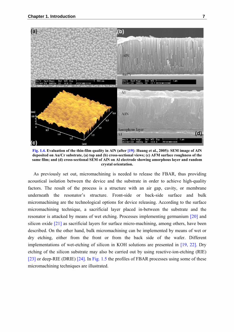
Taking the above-mentioned process parameters into consideration, the crystallographic quality of the AlN is evaluated by means of atomic force microscopy (AFM) and x-ray diffraction (XRD) characterization, among other techniques. AFM aids in measuring the granularity of the crystal, whereas XRD provides information on the preferred orientation of the crystal. Additional techniques like scanning electron microscopy (SEM) may also help in the visual inspection of the polycrystalline structure of the piezoelectric. The AFM and SEM images of Fig. 1.4(a) and Fig. 1.4(c); and Fig. 1.4(b) and Fig. 1.4(d) show surface and cross-sectional views of AlN crystals deposited on different substrates, respectively. It can be noted how different the AlN’s grain quality and the crystal orientation are when deposited under different conditions on Au/Cr (Fig. 1.4(b)) and Al (Fig. 1.4(d)) substrates [19].
Table 1.1. Electro-mechanical properties of some piezoelectric materials
Material Density (kg/m3)
Dielectric constant
Acoustic velocity
(m/s)
Acoustic impedance (106 kg/m2s)
Acoustic coupling
Acoustic loss dB/μs at 1 GHz
AlN 3270 8.5 10400 34.0 0.17 ~5 ZnO 5680 8.8 6330 36.0 0.28 8.3 CdS 4820 9.5 4465 21.5 0.15 >50
LiNbO3 4640 29 7320 30.6 0.17 0.5-0.9 LiTaO3 7450 43 6160 46.4 0.19 0.8
Chapter 1. Introduction 7
Fig. 1.4. Evaluation of the thin-film quality in AlN (after [19]: Huang et al., 2005): SEM image of AlN deposited on Au/Cr substrate, (a) top and (b) cross-sectional views; (c) AFM surface roughness of the same film; and (d) cross-sectional SEM of AlN on Al electrode showing amorphous layer and random
crystal orientation.
As previously set out, micromachining is needed to release the FBAR, thus providing acoustical isolation between the device and the substrate in order to achieve high-quality factors. The result of the process is a structure with an air gap, cavity, or membrane underneath the resonator’s structure. Front-side or back-side surface and bulk micromachining are the technological options for device releasing. According to the surface micromachining technique, a sacrificial layer placed in-between the substrate and the resonator is attacked by means of wet etching. Processes implementing germanium [20] and silicon oxide [21] as sacrificial layers for surface micro-machining, among others, have been described. On the other hand, bulk micromachining can be implemented by means of wet or dry etching, either from the front or from the back side of the wafer. Different implementations of wet-etching of silicon in KOH solutions are presented in [19, 22]. Dry etching of the silicon substrate may also be carried out by using reactive-ion-etching (RIE) [23] or deep-RIE (DRIE) [24]. In Fig. 1.5 the profiles of FBAR processes using some of these micromachining techniques are illustrated.

8 FBAR: fabrication, heterogeneous integration and sensor applications
Fig. 1.5. Different micromachining processes for releasing of FBAR: (a) surface, (b) front-side and (c) back-side bulk micromachining.
Less described is the influence of the electrodes’ layout in the FBAR’s performance. Some electrode geometries have been demonstrated to suppress or diminish spurious resonance modes better than others [25]. At the same time, the size of the electrodes has an effect on the electrical performance of FBARs [26, 27].
Tuning of FBARs is also of special interest. Due to process deviations or variation of the physical properties of the materials employed in the fabrication, the resonance frequency may be slightly different from that corresponding to the process design. Different approaches, such as electrostatic tuning [28], or mass-loading [29, 30], for example, have been conceived in order to change the resonance frequency of FBARs. Related to this topic, the temperature coefficient factor (TCF) of FBARs is also an important factor conditioning the performance of the device, especially for RF applications. Temperature-compensation strategies based on the deposition of an opposite-TCF thin-film material on the FBAR have been studied [31, 32].
The fabrication technology also conditions the final-user application of the FBAR. In the following section some of the most popular applications of FBAR are revisited.

Chapter 1. Introduction 9
1.3 FBAR applications FBAR finds application in a variety of systems ranging from radio-frequency (RF) to
sensing components. Although the telecommunication industry has been the very first engine stimulating the development of FBAR applications, new sensing applications have been demonstrated in the past few years. This can boost even more the increasing presence and importance of FBARs in the MEMS device and system markets, as reported by independent market forecasting, reproduced here in the diagram of Fig. 1.6 [33]. Nowadays, BAW devices (FBAR+SMR) represent over 90% of the RF MEMS share, which is roughly 10% of the RF MEMS market [34]. The BAW-based duplexer market is expected to grow from 300 million pieces in 2005 to a total demand of well over 900 million pieces in 2010. This represents revenues over US$1.5 billion by 2010. At this time, Agilent (FBAR) and Infineon (SMR) have market shares higher than 60% and 30%, respectively, of the total BAW device business.
Fig. 1.6. MEMS market presence trends: (a) MEMS market forecasting (after [33]: Electronics.ca Research Network, 2006); (b) RF MEMS market forecasting 2005-2009 (after [34]: WTC, 2005)
Nowadays, BAW devices (FBAR+SMR) represent over 90% of the RF MEMS share.
The demanding requirements of emerging third-generation (3G) mobile telecommunication systems have justified the search for new RF passive technologies, FBAR among them. All these systems operate in the 2 GHz frequency band, which is the typical FBAR’s resonance frequency (fabricated with a 1μm-thick AlN layer). The first RF applications of FBARs were thus devoted to supplying fully-passive components, able to compete with SAW and ceramic technologies, such as filters and duplexers. A duplexer is an RF system comprising two filters for simultaneous bidirectional communication, the first one being the transmission (TX) filter and the second one the reception (RX) filter. These components succeeded to offer lower-insertion losses, higher out-of-band rejection and a smaller size than those made with on-the-market technologies [35-41]. Also, FBAR’s temperature coefficients are in the order of -20 to -35 ppm/ºC, which is less than the typical range of -35 to -94 ppm/ºC of SAW devices. An FBAR-duplexer implementation from Agilent Technologies is shown in Fig. 1.7, where the

10 FBAR: fabrication, heterogeneous integration and sensor applications
six-FBAR layout (a), demonstration package system with two filter and assembly board (b), and insertion-loss electrical response of both TX and RX filters (c) are observed [4].
In FBAR-based sensor applications, one or more FBAR devices are the constituent elements of a system operating under piezoelectric actuation or detection mechanisms. Mass sensors, and biochemical, liquid or gas detectors, are some examples. All these applications work under the same principle of quartz crystal microbalances (QCM) [43]: mass loading of the resonator’s structure [44]. According to this principle, mass deposition on one of the FBAR electrodes gives rise to down-shifting of the resonance frequency, due to changes on the acoustic-impedance mismatching and consequent phase-shifting of the acoustic wave between the different FBAR-layer interfaces. The performance of mass-loading-based detectors is evaluated by means of mass sensitivity [Hz×cm2/ng] and the minimum detectable mass [ng/cm2]. Since the operating environment of the FBAR-based sensor determines its sensitivity and the Q-factor loading, different aspects of the fabrication process and resonance mode are considered. In this way, longitudinal or shear-mode operation is desired, depending on the sensing medium being air, gas or liquid.
Fig. 1.7. Agilent’s FBAR filter implementation (after [4, 42]: Agilent, 2001): (a) Layout of one of the six-FBAR filters of the duplexer [4]; (b) Demo package system comprising TX and RX FBAR-filters, assembly board and connectors [42]; and (c) Insertion-loss response of both TX and RX filters [4].

Chapter 1. Introduction 11
The 2GHz longitudinal-mode-FBAR biosensor system presented by Gabl et al. performs DNA and protein detection operating in a liquid environment [45]. An improved shear-mode FBAR version of the bio-detection system was also implemented by the same group. In this case, the sensor performance ruled by the smallest detectable mass attachment, is already better (2.3 ng/cm2) than that of QCMs [46]. Another electroacoustic chemical sensor based on FBAR detected low concentrations of the analyte upon exposure to H2, CO, and ethanol, with a fast and repeatable response [47]. An FBAR mass sensor at its tip, inserted into biological and chemical environments to sense various chemical-bio species, has shown to detect mercury ions in water [48]. Optical images of the sensor and schematic of the operating principle are shown in Fig. 1.8.
Based on the same metal-piezoelectric-metal structure and process of the FBAR, but operating at non-longitudinal resonance modes, different kinds of applications have recently appeared. For example, mechanically-coupled contour-mode MEMS filters using a thin-film AlN process have been demonstrated. The use of contour modes, whose frequencies are set by lithographically defined dimensions, permits the co-fabrication of multiple filters at arbitrary frequencies on the same chip, the filters having center frequencies of 40 and 100 MHz [49]. Also, a resonant mass sensor that is based on a lateral extensional mode (LEM) ZnO resonator, and has a minimum detectable mass (MDM) of 10-15g in air at room temperature, has been demonstrated by Pang et al. This resonator exhibits a quality factor higher than 1,400 at 60MHz, and mass detection uncertainty of only about 4.6×10⁻¹⁵g [50]. Some of these applications are shown in Fig. 1.9.
Fig. 1.8. Mass sensor for biological applications (after [48], Zhang et al., 2005): (a) Top and (b) bottom
view of the sensor and membrane; (c) schematic of the mercury-ion detecting principle (the ions interact with the coating gold, adding mass to the resonator and thus changing the resonance frequency).

12 FBAR: fabrication, heterogeneous integration and sensor applications
Fig. 1.9. Other FBAR-based applications (non-longitudinal resonance modes): (a) mechanically-coupled
contour-mode MEMS filters (after [49]: Stephanou et al., 2006); (b) Resonant mass sensor based on a lateral extensional mode (LEM) ZnO resonator (after [50]: Pang et al., 2006)
At this point, CMOS-integrated applications of FBARs have not been mentioned. Different integration philosophies, requirements, and fabrication processes have been conceived, and a detailed discussion about them is thoroughly presented in the following section.
1.4 MEMS-to-CMOS and FBAR-to-CMOS integration technologies
1.4.1 Importance and challenges of the CMOS-to-FBAR integration Over the last decades, CMOS has become the predominant fabrication technology for
integrated circuits (IC). Research and development efforts have been made to continuously improve process yield and reliability, while minimal feature sizes and fabrication costs continue to decrease. Nowadays, the power of CMOS technology is not only exploited for ICs but also for a variety of micro-sensors and MEMS benefiting from well established fabrication technologies and the availability of on-chip circuitry. Recently integrated micro-systems featuring calibration by digital programming, self-testing, and digital interfaces, have been implemented on-chip, demonstrating the strength of CMOS-based MEMS [51]. Nevertheless, the engineering of integration and process compatibility of MEMS to CMOS-based integrated circuit technologies is a tricky and challenging task at both technology and application levels. Several challenges like manufacturing temperature, packaging, and post-processing of MEMS, integrity of CMOS, and reliability and modeling of the MEMS-to-CMOS interface are just some of the considerations that can be mentioned [52-54].
1.4.2 Integration strategies Nowadays, hybrid and monolithic-integration are mainstream strategies in CMOS-to-
MEMS integration. More recently, heterogeneous integration has become an important evolution of the hybrid strategy in CMOS integration. According to the way in which the CMOS and the MEMS substrates are processed and interconnected, and assuming that the
Chapter 1. Introduction 13
same principles of MEMS integration are also suitable for FBAR integration, each strategy is defined as follows:
Hybrid: The MEMS chip is fabricated on a different substrate with various technological processes involving micromachining of the device’s structure, and combined with a separate standard CMOS integrated-circuit process. The integration of both processes is performed at the chip level by means of wire-bonding or soldering techniques after fabrication of both the MEMS and the CMOS chips (dicing is carried out prior to integration) [51].
Monolithic: The MEMS device and the IC are made and combined on a single substrate, according to the same standard, CMOS-compatible technology. The combination is performed using read-out circuitry to compensate for MEMS deficiencies or to provide the desired functionality. Depending on the order of fabrication, monolithic integration can be grouped into (1) Pre-CMOS (also known as “First-CMOS” or “Before-CMOS”), (2) Intermediate-CMOS (or interdigitated fabrication), and (3) Post-CMOS (add-on or “after-CMOS”) [51]:
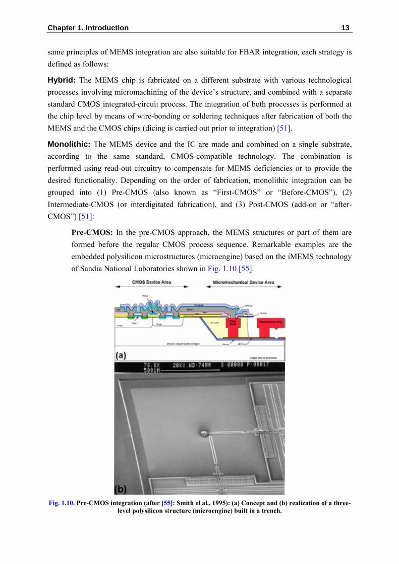
Pre-CMOS: In the pre-CMOS approach, the MEMS structures or part of them are formed before the regular CMOS process sequence. Remarkable examples are the embedded polysilicon microstructures (microengine) based on the iMEMS technology of Sandia National Laboratories shown in Fig. 1.10 [55].
Fig. 1.10. Pre-CMOS integration (after [55]: Smith el al., 1995): (a) Concept and (b) realization of a three-
level polysilicon structure (microengine) built in a trench.
14 FBAR: fabrication, heterogeneous integration and sensor applications
Intermediate CMOS: In the intermediate-CMOS approach, the CMOS process sequence is interrupted for additional thin-film deposition or micromachining steps. This approach is commonly exploited to implement surface micromachined polysilicon structures in CMOS technology. Either the standard gate polysilicon or an additional low-stress polysilicon layer is used as structural material. Examples of commercially available microsensors relying on intermediate process steps are the Infineon’s pressure-sensor integrated circuits [56].
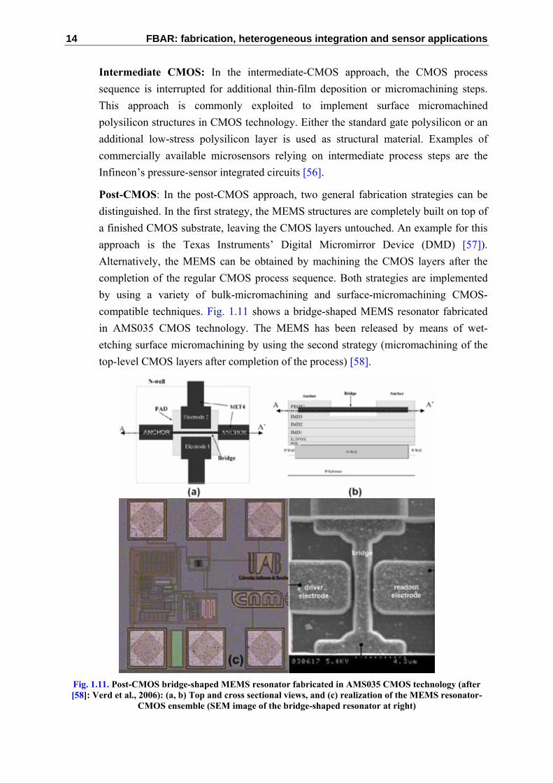
Post-CMOS: In the post-CMOS approach, two general fabrication strategies can be distinguished. In the first strategy, the MEMS structures are completely built on top of a finished CMOS substrate, leaving the CMOS layers untouched. An example for this approach is the Texas Instruments’ Digital Micromirror Device (DMD) [57]). Alternatively, the MEMS can be obtained by machining the CMOS layers after the completion of the regular CMOS process sequence. Both strategies are implemented by using a variety of bulk-micromachining and surface-micromachining CMOS-compatible techniques. Fig. 1.11 shows a bridge-shaped MEMS resonator fabricated in AMS035 CMOS technology. The MEMS has been released by means of wet-etching surface micromachining by using the second strategy (micromachining of the top-level CMOS layers after completion of the process) [58].
Fig. 1.11. Post-CMOS bridge-shaped MEMS resonator fabricated in AMS035 CMOS technology (after [58]: Verd et al., 2006): (a, b) Top and cross sectional views, and (c) realization of the MEMS resonator-
CMOS ensemble (SEM image of the bridge-shaped resonator at right)
Chapter 1. Introduction 15
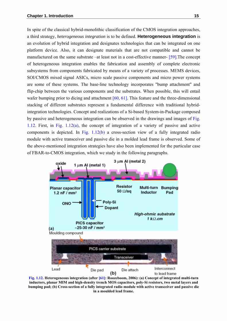
In spite of the classical hybrid-monolithic classification of the CMOS integration approaches, a third strategy, heterogeneous integration is to be defined. Heterogeneous integration is an evolution of hybrid integration and designates technologies that can be integrated on one platform device. Also, it can designate materials that are not compatible and cannot be manufactured on the same substrate –at least not in a cost-effective manner- [59].The concept of heterogeneous integration enables the fabrication and assembly of complete electronic subsystems from components fabricated by means of a variety of processes. MEMS devices, SOI/CMOS mixed signal ASICs, micro scale passive components and micro power systems are some of these systems. The base-line technology incorporates "bump attachment" and flip-chip between the various components and the substrates. When possible, this will entail wafer bumping prior to dicing and attachment [60, 61]. This feature and the three-dimensional stacking of different substrates represent a fundamental difference with traditional hybrid-integration technologies. Concept and realizations of a Si-based System-in-Package composed by passive and heterogeneous integration can be observed in the drawings and images of Fig. 1.12. First, in Fig. 1.12(a), the concept of integration of a variety of passive and active components is depicted. In Fig. 1.12(b) a cross-section view of a fully integrated radio module with active transceiver and passive die in a molded lead frame is observed. Some of the above-mentioned integration strategies have also been implemented for the particular case of FBAR-to-CMOS integration, which we study in the following paragraphs.
Fig. 1.12. Heterogeneous integration (after [61]: Roozeboom, 2006): (a) Concept of integrated multi-turn inductors, planar MIM and high-density trench MOS capacitors, poly-Si resistors, two metal layers and bumping pad; (b) Cross-section of a fully integrated radio module with active transceiver and passive die
in a moulded lead frame.

16 FBAR: fabrication, heterogeneous integration and sensor applications
1.4.3 Historical development of the FBAR-to-CMOS integration The integration of FBAR has a relatively short history, compared to other MEMS devices.
As a high-Q factor device, FBARs have also attracted the attention of RF integrated-circuit and sensor-application designers. Recent developments in FBAR-to-CMOS integration have stimulated the conception of integrated applications in which FBAR is a key component, whose IC integration is a requirement for proper functionality of the system. Hybrid and monolithic integration strategies have been investigated and implemented so far.
In the case of hybrid integration, the FBAR and IC chips are bonded to their corresponding circuit nodes. Examples of this integration approach are the oscillators presented in [62-64], where the FBAR performs the crystal-like functionality in the system. In Fig. 1.13 the UC Berkeley-Agilent’s implementation of a Pierce oscillator is shown. Double and short wire-bonding between both chips ensures reduction of losses and parasitic inductances. Area restrictions, added parasitic capacitances due to the bonding, and batch processing of the integrated devices are some of the limitations of the hybrid integration approach.
In the current art of monolithic integration, the FBAR has been placed above the circuit using a post-CMOS strategy, thus saving die area. This approach was disclosed in 1993 [65], and a system integrating FBAR and radio circuitry was conceived in 2001 [66]. However, it was as late as 2005 when the first monolithic FBAR-above-IC RF systems were demonstrated by the Martina consortium. Using a 0.25 μm BiCMOS process, this group implemented double-lattice filters [67], filtering LNAs comprising two broadband amplifiers and one FBAR filter [68], and a 5GHz FBAR-based low-phase noise oscillator [69], among others, as shown in Fig. 1.14.
Fig. 1.13. Hybrid integration of FBAR with low-power CMOS oscillator (after [62]: Otis and Rabaey,
2003)

Chapter 1. Introduction 17
The interest in monolithic integration of FBAR has not been limited to fully-active ICs, but also to passive components like CMOS inductors [70]. On the other hand, CMOS-integrated MEMS, NEMS and SAW resonators have already been demonstrated as well [71-73]. In spite of the elegance of monolithic integration, its complexity, compatibility issues, costs and technology-specific nature are some of the main challenges of this approach.
Fig. 1.14. Post-CMOS monolithic integration of FBAR (after [68]: Carpentier el al., 2005): (a) Martina’s concept of the FBAR-above-IC integration; (b) Filtering LNA comprising two broadband amplifiers and
differential-lattice filter.

18 FBAR: fabrication, heterogeneous integration and sensor applications
1.5 Motivation and purpose of this thesis The review made in previous sections shows that considerable effort has been made to
develop FBAR fabrication technologies and their applications and, at the same time, to define FBAR-to-CMOS integration processes compatible with standard CMOS technologies. Thus, from previous art some remarks can be made:
1. FBAR fabrication technologies have reached a phase of maturity and are well established at the industrial manufacturing level. Recent development of FBARs has been more oriented to refining the fabrication processes, in order to produce devices with enhanced spurious-mode rejection, lower temperature coefficients, and tuning capability, among other features.
2. Hybrid and monolithic integrations of FBARs to CMOS integrated-circuit technologies have already been demonstrated. In the case of monolithic integration, this has only been achieved in the context of specific developments for the involved CMOS technology. In other words, the process conditions required for this achievement are not necessarily applicable for the general case of a variety of CMOS processes. No prior FBAR-CMOS heterogeneous integration has been reported.
3. Mainly due to RF applications, FBARs have conquered a big share of the MEMS market. Agilent Technologies and Infineon AG are the main manufacturing companies of FBAR-based filters and duplexers. More recently, efforts are being made by these companies to develop integrated, FBAR-based commercial oscillators. On the other hand, sensor applications of FBARs have emerged, in spite of the RF application dominance. Concept demonstration of the FBAR as a mass, fluid or gas detector has proven to be attractive for sensing systems. Most of these systems are in early stages of their development. New sensing applications are still to be developed.
Taking the previous remarks into account, FBAR development has still a long technological way to go. Three aspects have been the main motivation for me to initiate this thesis:
1. In spite of the maturity of FBAR technology, there is still more space for research work on the optimization of the FBAR manufacturing technology. This implies that the details of the “standard” FBAR fabrication process should be known before opening new research avenues. Materials, fabrication processes and physical principles behind FBAR are interesting study topics in themselves. Among these topics, for example, novel tuning procedures can be mentioned.
2. The convergence of MEMS, electronics and other technologies demands a reduction in size and power consumption of application systems. FBAR-to-CMOS integration is a requirement for further development of the system-on-a-chip concept. Although very

Chapter 1. Introduction 19
sophisticated, current-art integration techniques are still technology-specific, complex and costly.
3. The high Q-factors and mass-sensitivity of FBARs justify the exploration of new, state-of-the-art applications, specifically in the growing field of FBAR-based sensing systems. Therefore, FBAR should be a key technology towards the nano-bio-info convergence (NBIC).
Previous experiences of CNM-CSIC, UAB and LIRMM in MEMS-to-CMOS fabrication, integration, and modeling, have also motivated a thesis on the FBAR field. Furthermore, EPSON has gotten involved in the development of MEMS-to-CMOS integration as an industrial partner of the CNM and UAB. Beginning with the “R434 project”, which was intended for monolithic MEMS-CMOS integration towards 434MHz systems [74, 75], the collaboration rapidly evolved to the development of the FBAR technology at CNM.
With regard to acoustic resonator and crystal technologies, EPSON is a well-recognized world player in quartz-based and SAW devices. Nowadays, they intend to strengthen their position in the BAW-FBAR market. For that reason, a new path of research collaboration aiming to the development of the FBAR’s technology was created through the DELFOS project, which was funded by Seiko EPSON Corporation and EPSON Europe Electronics GmbH. At the same time, this collaboration allowed CNM to develop the AlN deposition, compatibility and patterning technologies, which were not available prior to the launch of the DELFOS project. The main goals of the CNM-UAB-EPSON collaboration within this project were: 1) to develop the FBAR’s fabrication technology; 2) to study the FBAR’s materials and process providing CMOS compatibility; and 3) to develop on-system applications of FBAR.
In regard to the foregoing experiences and motivation, the contributions of this thesis have been mainly focused on the development of:
1. The FBAR fabrication technology and characterization techniques, thus exploring the piezoelectric layer deposition, the piezoelectric-to-CMOS compatibility, and the micromachining techniques, among others.
2. More flexible, versatile, cheap and technology-open FBAR-to-CMOS heterogeneous integration strategies, through the implementation of a variety of principles and fabrication techniques towards the FBAR-CMOS compatibility.
3. New applications of FBARs, mainly in the sensing-system field. These applications are based on the above-mentioned FBAR technology.
Regarding the first contribution, additional efforts on process and layout-design in order to improve the FBAR’s performance must also be accounted for. This optimization concerns the design and fabrication of devices with reduced temperature coefficients, for example. Also,

20 FBAR: fabrication, heterogeneous integration and sensor applications
the exploration of novel tuning techniques is a relevant contribution from the technological point of view.
1.6 Outline of this thesis This thesis addresses the development of the FBAR fabrication technology in order to
propose new applications and reduce the complexity of FBAR-to-CMOS integration.
In Chapter 2, the technological aspects of FBAR fabrication are covered. The AlN deposition technology on metal substrates and the micromachining techniques are described, and the fabrication compatibility of the metal and AlN patterning is discussed. Also, the design and fabrication of temperature-compensated FBARs are studied. Different characterization techniques like AFM, XRD, SEM, and Confocal, have been used in the analysis of AlN and the FBAR’s structure, and they are described in this chapter.
Experimental and simulation works on device characterization, modeling and optimization are presented in Chapter 3. Fundamental concepts and experimental set-up of RF electrical characterization of FBAR are defined. Characterization results are presented and contrasted with equivalent-circuit modeling for a variety of devices with different layout and sizes. On the modeling side, a parameter-extraction algorithm was developed, and its implementation details are explained in this chapter. Last but not least, a novel focused-ion-beam-assisted technique for tuning of FBAR is introduced in this section too.
Chapter 4 deals with the technology development of the heterogeneous integration of FBAR with CMOS technologies. Since this is a central topic of the thesis, special attention has been given to presenting the method, fabrication process and materials, and characterization results of the FBAR-CMOS integrated system in detail. Compared to previous art achievements, a discussion on the key contributions and challenges of this technology is initiated. Heterogeneous FBAR-to-CMOS-integration represents one of the main contributions of this work.
In Chapter 5 various FBAR-based sensor applications are introduced to the reader. The chapter begins with an explanation of the principles and performance of a distributed-mass sensor, to continue more in depth with the description and analysis of a novel, FBAR-based localized-mass sensor. Different aspects regarding the superiority of this technology compared to other mass-detection systems are covered. Also, acoustic and finite-element modeling of the sensor is proposed and the characterization and modeling results are contrasted. Mechanical sensors based on FBAR and, more specifically, accelerometer and force sensors are the second group of applications contributed by this work. A detailed description of the additional fabrication processes of the technology is given. A new kind of contact-free piezoelectric resonator is the third application presented in this work. This device is based on a surface micro-machining process, and the main aspects involving its layout and performance are discussed.
Chapter 1. Introduction 21
Finally, Chapter 6 concludes with a summary of the activities and achievements of the thesis. Research lines for future work on the FBAR field are suggested.
References 1 K. M. Lakin and J. S. Wang, “Acoustic bulk wave composite resonators”, Applied Physics Lett. 38
(1981) 125-127.
2 G.V. Tsarenkov, “10+ GHz BAW resonators based on semiconductor multilayer heterostructures”, in Proc. IEEE Intl. Ultrason. Symp. 1999, Oct. 17-19, 1999, Caesars Tahoe, NV, USA, 939-942.
3 M.-C. Chao, Z.-N. Huang, S.-Y. Pao, Z. Wang, and C.S. Lam, “Modified BVD-equivalent circuit of FBAR by taking electrodes into account”, in Proc. IEEE Intl. Ultrason. Symp. 2002, Oct. 8-12, 2002, Munich, Germany, 973-976.
4 W. Mueller, “A brief overview of FBAR technology”, Agilent Technologies (technical report AB-WCM200701a), July 20, 2001.
5 ANSI/IEEE Std. 176-1987, “IEEE Standard on Piezoelectricity”. The Institute of Electrical and Electronics Engineers, Inc, 1988, New York, NY, USA.
6 EPSON Toyocom, “SAW device principles”. Available on-line (accessed November 2007): http://www.epsontoyocom.co.jp/english/tech/tech_set.html
7 K.M. Lakin, G.R. Kline, and K.T. McCarron, “Development of miniature filters for wireless applications”, IEEE T. Microwave Theory Techniques 43 (1995) 2933-2939.
8 R. Aigner, "Volume manufacturing of BAW-filters in a CMOS fab", in Proc. Second International Symposium on Acoustic Wave Devices for Future Mobile Communication Systems, 3-5 March 2004, Chiba, Japan, 129-134.
9 N.W. Emanetoglu, S. Muthukumar, P. Wu, R. Wittstruck, and Y. Lu, “MgxZn1-xO: A New Piezoelectric Material”, in Proc. IEEE Intl. Ultrason. Symp. 2001, 1, 7-10 October, 2001, Atlanta, GA, USA, 253-256.
10 H. Fritze, and H. L. Tuller, “Langasite for high-temperature bulk acoustic wave applications”, Appl. Physics Lett. 78, 7 (2001) 976-977.
11 F. Engelmark, G.F. Iriarte, I.V. Katardjiev, M. Ottosson, P. Muralt, and S. Berg, “Structural and electroacoustical studies of AlN thin films during low temperature radio frequency sputtering deposition”, J. Vac. Sci. Technol. A 19 (2001) 2664-2669.
12 T. Shiosaki, T. Yamamoto, T. Oda, K. Harada, and A. Kawabata, “Low temperature growth of piezoelectric films by RF reactive planar magnetron sputtering”, Jap. J. Appl. Phys. 20 (1981) 149-152.
13 S. Uchiyama, Y. Ishigami, M. Ohta, M. Niigaki, H. Kan, Y. Nakanishi, and T. Yamaguchi, “Growth of AlN films by magnetron sputtering”, J. Crystal Growth 189-190 (1998), 448-451.
14 R. D. Vispute, Hong Wu, and J. Narayan, “High quality epitaxial aluminum nitride layers on sapphire by pulsed laser deposition”, Appl. Physics Lett. 67, 11 (1995) 1549-1551.
15 M.-A. Dubois and P. Muralt, “Stress and piezoelectric properties of aluminum nitride thin films deposited onto metal electrodes by pulsed direct current reactive sputtering”, J. Appl. Physics 89, 11 (2001) 6389-6395.
16 L. Shen, R.K. Fu, and P.K. Chu, “Synthesis of aluminum nitride films by plasma immersion ion implantation–deposition using hybrid gas–metal cathodic arc gun”, Rev. Scient. Instrum.75 (2004) 719-724.

22 FBAR: fabrication, heterogeneous integration and sensor applications
17 J.-B. Lee, J.-P. Jung, M.-H. Lee, and J.-S. Park, “Effects of bottom electrodes on the orientation of AlN films and the frequency responses of resonators in AlN-based FBARs”, Thin Solid Films 447 –448 (2004) 610-614.
18 M. Akiyama, K. Nagao, N. Ueno, H. Tateyama, and T. Yamada, “Influence of metal electrodes on crystal orientation of aluminum nitride thin films”, Vacuum 74 (2004) 699-703.
19 C.-L. Huang, K.-W. Tay, and L. Wu, “Fabrication and performance analysis of film bulk acoustic wave resonators”, Mater. Lett. 59 (2005) 1012-1016.
20 M. Hara, J. Kuypers, T. Abe, and M. Esashi, “Surface micromachined AlN thin film 2 GHz resonator for CMOS integration”, Sens. Actuator A-Phys. 117 (2005) 211-216.
21 S. Saravanan, E. Berenschot, G. Krijnen, and M. Elwenspoek, “A novel surface micromachining process to fabricate AlN unimorph suspensions and its application for RF resonators”, Sens. Actuator A-Phys. 130–131 (2006) 340-345.
22 W. Pang, H. Zhang, and E.S. Kim, “Micromachined acoustic wave resonator isolated from substrate”, IEEE T. Ultrason. Ferroelectr. Freq. Control 52 (2005) 1239-1246.
23 G. Piazza, P.J. Stephanou, J.P. Black, R.M. White, and A.P. Pisano, “Single-chip multiple-frequency RF microresonators based on aluminum nitride contour-mode and FBAR technologies”, in Proc. IEEE Intl. Ultrason. Symp. 2005, Sept. 18-21 2005, Rotterdam, The Netherlands, 1187-1190.
24 Y. Satoh, T. Nishihara, T. Yokoyama, M. Iwaki, and T. Miyashita, “Development of 5GHz FBAR Filters for Wireless Systems”, in Proc. Second International Symposium on Acoustic Wave Devices for Future Mobile Communication Systems, 3-5 March 2004, Chiba, Japan, 141-144.
25 D. Rosén, J. Bjursttröm, and I. Katardjiev, “Suppression of spurious lateral modes in thickness-excited FBAR resonators”, IEEE T. Ultrason. Ferroelectr. Freq. Control 52 (2005) 1189-1192.
26 Y.-D. Kim, K.-H. Sunwoo, S.-C. Sul, J.-H. Lee, D.-H. Kim, I.-S. Song, S.-H. Choa, and J.-G. Yook, “Highly Miniaturized RF Bandpass Filter Based on Thin-Film Bulk Acoustic-Wave Resonator for 5-GHz-Band Application”, IEEE T. Microw. Theory Tech. 54 (2006) 1218-1228.
27 Q. Su, P. Kirby, E. Komuro, M. Imura, Q. Zhang, and R. Whatmore, “Thin-film bulk acoustic resonators and filters using ZnO and lead–zirconium–titanate thin films”, IEEE T. Microw. Theory Tech. 49 (2001) 769-778.
28 W. Pan, P. Soussan, B. Nauwelaers, and H.A.C. Tilmans, “A surface micromachined electrostatically tunable film bulk acoustic resonator”, Sens. Actuator A-Phys. 126 (2006) 436-446.
29 R. C. Ruby and P. P. Merchant, “Tunable thin film acoustic resonators and method for making the same”, U.S. Patent No. 5587620, 24 Dec. 1996.
30 M. A. Ylilammi, “Method for performing on-wafer tuning of thin film bulk acoustic wave resonators (FBARS)”, U.S. Patent No. 6051907, 18 Apr. 2000.
31 F. Vanhelmont, P. Philippe, A.B.M. Jansman, R.F. Milsom, J.J.M. Ruigrok, and A. Oruk, “A 2 GHz Reference Oscillator incorporating a Temperature Compensated BAW Resonator”, in Proc. IEEE Intl. Ultrason. Symp. 2006, Oct. 3-6 2006, Vancouver, Canada, 333-336.
32 J.D. Larson III, “Acoustic wave resonator and method of operating the same to maintain resonance when subjected to temperature variations”, US Patent no. 6,420,820, July 16, 2002.
33 Susie Inouye, Electronics.ca Research Network, 2006 MicroElectroMechanical Systems (MEMS) (Research Report # DB2563), p. 1-48, November 2006.
34 WTC Wicht Technologie Consulting, "RF MEMS Market II, 2005-2009", 2005.
Chapter 1. Introduction 23
35 P. Bradley, R. Ruby, J. Larson III, Y. Oshymanky, and D. Figueredo, "A Film Bulk Acoustic Resonator (FBAR) duplexer for USPCS handset applications", in IEEE International Microwave Symp. MTT-S 2001 Digest of Tech. Papers, May 20-25 2001, Phoenix, AZ, USA, pp. 367-370.
36 R. Ruby, P. Bradley, J. Larson III, Y. Oshmyanski, and D. Figueredo, “Ultra-Miniature High-Q Filters and Duplexers Using FBAR Technology”, in IEEE Intl. Solid-State Circuits Conf. Dig. of Tech. Papers, Feb. 5-7 2001, San Francisco, CA, USA, 120-121.
37 K.M. Lakin, J.R. Belsick, J.P. McDonald, K.T. McCarron, and C.W. Andrus, "Bulk Acoustic Wave Resonators And Filters For Applications Above 2 GHz", in IEEE International Microwave Symp. MTT-S 2002 Digest of Tech. Papers, Jun. 3-7 2002, Seattle, WA, USA, 3, 1487-1490.
38 M. Ylilammi, J. Ella, M. Partanen, and J. Kaitila, "Thin Film Bulk Acoustic Wave Filter", IEEE T. Ultrason. Ferroelectr. Freq. Control 49, 4 (2002) 535-539.
39 T. Nishihara, T. Yokohama, T. Miyashita, and Y. Satoh, “High Performance and Miniature Thin Film Bulk Acoustic Wave Filters for 5 GHz”, in Proc. IEEE Intl. Ultrason. Symp. 2002, Oct. 8-12, 2002, Munich, Germany, 969-972.
40 H. Morkner, R. Ruby, M. Frank, and D. Figueredo, "An integrated FBAR filter and PHEMT switched-amp for wireless applications", in IEEE International Microwave Symp. MTT-S 1999 Digest of Tech. Papers, Jun. 13-19 1999, Anaheim, CA, USA, 4, 1393-1396.
41 D. Feld, K. Wang, P. Bradley, A. Barfknecht, B. Ly, and R. Ruby, "A high performance 3.0 mm x 3.0 mm x 1.1 mm FBAR full band Tx filter for US PCS handsets", in Proc. IEEE Intl. Ultrason. Symp. 2002, Oct. 8-12, 2002, Munich, Germany, 913-918.
42 Applications Engineering Team, Personal Systems Division, “Using the HPMD-series and QPMD-series CDMA duplexers”, in Design Tip (technical report), Agilent Technologies, 12 April 2002.
43 C. S. Lu, “Applications of Piezoelectric Quartz Crystal Microbalance”, Elsevier, London, 1984.
44 G.Z. Sauerbrey, Verwendung von Schwingquarzen zur Wägung dünner Schichten und Microwägung, Z. Phys. 155 (1959) 206–222.
45 R. Gabl, H.-D. Feucht, H. Zeininger, G. Eckstein, M. Schreiter, R. Primig, D. Pitzer, and W. Wersing, “First results on label-free detection of DNA and protein molecules using a novel integrated sensor technology based on gravimetric detection principles”, Biosens. Bioelectron. 19 (2004) 615–620.
46 J. Weber, W.M. Albers, J. Tuppurainen, M. Link, R. Gabl, W. Wersing, and M. Schreiter, “Shear mode FBARs as highly sensitive liquid biosensors”, Sens. Actuator A-Phys. 128 (2006) 84–88.
47 M. Benetti, D. Cannat`a, F. Di Pietrantonio, V. Foglietti, and E. Verona, “Microbalance chemical sensor based on thin-film bulk acoustic wave resonators”, Appl. Phys. Lett. 87 (2005) 173504.
48 H. Zhang, M.S. Marma, E.S. Kim, C.E. McKenna, and M.E. Thompson, “A film bulk acoustic resonator in liquid environments”, J. Micromech. Microeng. 15 (2005) 1911–1916.
49 P.J. Stephanou, G. Piazza, C.D. White, M.B.J. Wijesundara and A.P. Pisano, “Mechanically coupled contour mode piezoelectric aluminum nitride MEMS filters”, in Proc. IEEE Intl. Conf. MEMS 2006, Istambul, Turkey, 22-26 January 2006, 906-909.
50 W. Pang, L. Yan, H. Zhang, H. Yu, E.S. Kim, and W.C. Tang, “Ultrasensitive mass sensor based on lateral extensional mode (LEM) piezoelectric resonator”, in Proc. IEEE Intl. Conf. MEMS 2006, Istambul, Turkey, 22-26 January 2006, 78-81.
51 H. Baltes, O. Brand, A. Hierlemann, D. Lange, and C. Hagleitner, "CMOS MEMS – Present and future", Proc. IEEE Intl. Conf. MEMS 2002, 220-24 January 2002, Las Vegas, NV, USA, 459-466.

24 FBAR: fabrication, heterogeneous integration and sensor applications
52 N. H. Tea, V. Milanovic, C. A. Zincke, J. S. Suehle, M. Gaitan, M. E. Zaghloul, and J. Geist, “Hybrid postprocessing etching for CMOS-compatible MEMS”, J. Microelectromech. Syst. 6 (1997) 363-372.
53 L. Latorre, P. Nouet, Y. Bertrand, P. Hazard, and F. Pressecq, “Characterization and modeling of a CMOS-compatible MEMS technology,” Sens. Actuator A-Phys. 74 (1999) 1-3, 143-147.
54 J. L. Lund, C. V. Jahnes, H. Deligianni, L. Paivikki Buchwalter, J. M. Cotte, P. Andricacos, D. E. Seeger, and J. H. Magerlein, “A low temperature Bi-CMOS compatible process for MEMS RF resonators and filters”, in Proc. Solid-State Sensor, Actuator and Microsystems Workshop 2002, Hilton Head Island, South Carolina, June 2-6, 2002, 38-41.
55 J.H. Smith, S. Montague, J.J. Sniegowski, J.R. Murray and P.J. McWhorter, “Embedded micromechanical devices for the monolithic integration of MEMS with CMOS”, In Proc. IEEE Intl. Electron Devices Meeting IEDM 1995, Dec. 10-13 1995, Washington, DC, USA, 609-612.
56 C. Hierold, “Intelligent CMOS sensors”, in Proc. IEEE Intl. Conf. MEMS 2000, 23-27 January 2000, Miyazaki, Japan, 1-6.
57 J. M. Florence, and L.A. Yoder, “Display system architectures for digital micromirror device (DMD)-based”, in Proc. SPIE Projection Displays II, Jan. 29 1996, San Jose CA, USA, 2650, 193-208.
58 J. Verd, A. Uranga, J. Teva, J. L. López, F. Torres, J. Esteve, G. Abadal, F. Pérez-Murano, and N. Barniol, “Integrated CMOS–MEMS with on-Chip readout electronics for high-frequency applications”, IEEE Electron Dev. Lett. 27 (2006), 495-497.
59 IBM Zurich Research Laboratory. “Device Integration”. Available on-line (accessed November 2007): http://www.zurich.ibm.com/st/server/microdevice.html
60 J. Geske, Y.L. Okuno, J.E. Bowers, and V. Jayaraman, “Vertical and lateral heterogeneous integration”, Appl. Phys. Lett. 79 (2001) 1760-1762.
61 F. Roozeboom, A.L.A.M. Kemmeren, J.F.C. Verhoeven, F.C. van den Heuvel, J. Klootwijk, H. Kretschman, T. Frič, E.C.E. van Grunsven, S. Bardy, C. Bunel, D. Chevrie, F. LeCornec, S. Ledain, F. Murray and P. Philippe, “Passive and heterogeneous integration towards a Si-based System-in-Package concept”, Thin Solid Films 504 (2006), 391-396.
62 B. P. Otis, and J. M. Rabaey, “A 300-μW 1.9-GHz CMOS oscillator utilizing micromachined resonators”, IEEE J. Solid-State Circuits 38 (2003) 1271-1274.
63 Y. H. Chee, A. M. Niknejad, and J. M. Rabaey, “An ultra-low-power injection locked transmitter for wireless sensor networks”, IEEE J. Solid State Circuits 41 (2006) 1740-1748.
64 H. Zhang, J. Kim, W. Pang, H. Yu, and S. Kim, “5GHz low phase-noise oscillator based FBAR with low TCF”, in Proc. 13th International Conference on Solid-State Sensors, Actuators and Microsystems Transducers 2005, Jun. 5-9 2005, Seoul, Korea, 1100-1101.
65 W. C. Dunn, H. Ming Liaw, L. Ristic, and R. M. Roop, “Monolithic circuit with integrated bulk structure resonator”, U.S. patent no. 5,260,596, Nov. 1993.
66 K. Lee, Y. S. Eo, and S. Hyun, “Single-chip radio structure with piezoelectric crystal device integrated on monolithic integrated circuit and method of fabricating the same”, U.S. patent no. 6,285,866, Sep. 2001.
67 M.-A. Dubois, C. Billard, C. Muller, G. Parat, and P. Vincent, “Integration of high-Q BAW resonators and filters above IC”, in IEEE Intl. Solid-State Circuits Conf. Dig. of Tech. Papers, 2005, Feb. 6-10 2005, San Francisco CA, USA, 392-393.
68 J.F. Carpentier, A. Cathelin, C. Tilhac, P. Garcia, P. Persechini, P. Conti, P. Ancey, G. Bouche, G. Caruyer, D. Belot, C. Arnaud, C. Billard, G. Parat, J.B. David, P. Vincent, M.A. Dubois, and C. Enz, "A SiGe:C BiCMOS WCDMA zero-IF RF front-end using an above-IC BAW filter", in

Chapter 1. Introduction 25
IEEE Intl. Solid-State Circuits Conf. Dig. of Tech. Papers, 2005, Feb. 6-10 2005, San Francisco CA, USA, 394-395.
69 M. Aissi, E. Tournier, M. A. Dubois, C. Billard, H. Ziad, and R. Plana, "A 5 GHz above-IC FBAR low phase noise balanced oscillator", in Proc. IEEE Radio Frequency Integrated Circuits Symposium RFIC-2006, Jun. 11-13, 2006, San Francisco CA, USA, 1, 25-28.
70 D. Figueredo, R. C. Ruby, Y. Oshmyansky, and P. Bradley, “Thin film bulk acoustic resonator (FBAR) and inductor on a monolithic substrate and method of fabricating the same”, U.S. patent no. 6,710,681, Mar. 2004.
71 M. Furuhata, A. Yajima, K. Goto, H. Sato, T. Funasaka, S. Kawano, S. Fujii, T. Higuchi, M. Ueno, “Development of Monolithic CMOS-SAW Oscillator”, in Proc. IEEE Intl. Ultrason. Symp., 2005, Sept. 18-21, 2005, Rotterdam, The Netherlands, 4, 2194-2197.
72 E. Forsen, G. Abadal, S. Ghatnekar-Nilsson, J. Teva, J. Verd, R. Sandberg, W. Svendsen, F. Perez-Murano, J. Esteve, E. Figueras, F. Campabadal, L. Montelius, N. Barniol, and A. Boisen, “Ultrasensitive mass sensor fully integrated with complementary metal-oxide-semiconductor circuitry”, Appl. Phys. Lett. 87 (2005) 043507-1-3.
73 B. Ilic, H. G. Craighead, S. Krylov, W. Senaratne, C. Ober, and P. Neuzil, “Attogram detection using nanoelectromechanical oscillators”, J. Appl. Phys. 95 (2004) 3694-3703.
74 A. Uranga, H. Campanella, N. Barniol, J. Esteve, L. Terés, Z. Davis. “A Read-Out Strategy and Circuit Design for High Frequency MEMS Resonators”, in Proc. IEEE International Symposium on Circuits and Systems 2005 ISCAS 2005, May 23-26, 2005, Kobe, Japan, 5361-5364.
75 H. Campanella, A. Uranga, Z. Davis, J. Esteve, L. Terés, N. Barniol. “Band-pass transimpedance read out circuit for UHF MEMS resonator applications”, in Proc. SPIE Symposium on Microtechnologies for the New Millennium 2005, Sevilla, Spain, May 9-11, 2005, 5837, 300-309.

CHAPTER 2
Development of the FBAR fabrication technology
The main processes involved in the fabrication of FBARs are the piezoelectric layer and metal
layers deposition and patterning, and the micro-machining technology for resonator’s releasing. Nowadays, various technological options and combinations can be employed for implementing these processes in order to obtain high-quality factor devices. In this chapter, the development of the fabrication technology of FBAR devices within the in-house CNM25 process is presented.
First, an overview of the FBAR’s fabrication processes implemented by this work is presented in section 2.1. In section 2.2 the aluminum nitride (AlN) layer deposition technology and material’s characterization results are described. Next, in section 2.3 the experiments and testing to obtain a compatible technology between deposition, etching, lift-off and micromachining of the different process layers are explained. As a result of the compatibility development, fully-released devices have been fabricated. By using scanning-electron-microscope (SEM), interferometer and confocal inspection techniques, the FBAR’s structural analysis was carried out. The implementation of these techniques and the conclusions of the analysis are discussed in section 2.4.
2.1 Process overview Three different processes were designed for implementing the FBAR fabrication. The
micromachining technology and the materials of the electrodes and passivation layers are the main variations differentiating each process. By means of the in-house CNM25 process, FBARs were implemented as a sandwiched aluminum nitride (AlN) membrane (1μm-thick), sputtered on top of a platinum (Pt) layer (150nm-thick), and fabricated on a silicon (Si) substrate. Devices were released by one of three micromachining techniques in order to obtain a free-moving device. Both the top and bottom electrodes were fabricated using Pt of the same thicknesses, although an extra metal layer is added to allow proper adhesion of the Pt. Depending on the micromachining technique, the adhesive metals may be titanium (Ti) or chromium (Cr), which were typically implemented with thickness of 30nm. Additionally, a passivation layer was deposited on top of the silicon substrate, prior to bottom electrode’s deposition. The passivation layer provides a window for etching and reduces the electrical
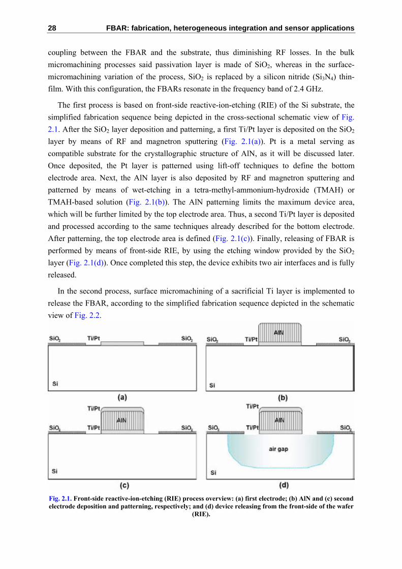
28 FBAR: fabrication, heterogeneous integration and sensor applications
coupling between the FBAR and the substrate, thus diminishing RF losses. In the bulk micromachining processes said passivation layer is made of SiO2, whereas in the surface-micromachining variation of the process, SiO2 is replaced by a silicon nitride (Si3N4) thin-film. With this configuration, the FBARs resonate in the frequency band of 2.4 GHz.
The first process is based on front-side reactive-ion-etching (RIE) of the Si substrate, the simplified fabrication sequence being depicted in the cross-sectional schematic view of Fig. 2.1. After the SiO2 layer deposition and patterning, a first Ti/Pt layer is deposited on the SiO2 layer by means of RF and magnetron sputtering (Fig. 2.1(a)). Pt is a metal serving as compatible substrate for the crystallographic structure of AlN, as it will be discussed later. Once deposited, the Pt layer is patterned using lift-off techniques to define the bottom electrode area. Next, the AlN layer is also deposited by RF and magnetron sputtering and patterned by means of wet-etching in a tetra-methyl-ammonium-hydroxide (TMAH) or TMAH-based solution (Fig. 2.1(b)). The AlN patterning limits the maximum device area, which will be further limited by the top electrode area. Thus, a second Ti/Pt layer is deposited and processed according to the same techniques already described for the bottom electrode. After patterning, the top electrode area is defined (Fig. 2.1(c)). Finally, releasing of FBAR is performed by means of front-side RIE, by using the etching window provided by the SiO2 layer (Fig. 2.1(d)). Once completed this step, the device exhibits two air interfaces and is fully released.
In the second process, surface micromachining of a sacrificial Ti layer is implemented to release the FBAR, according to the simplified fabrication sequence depicted in the schematic view of Fig. 2.2.
Fig. 2.1. Front-side reactive-ion-etching (RIE) process overview: (a) first electrode; (b) AlN and (c) second electrode deposition and patterning, respectively; and (d) device releasing from the front-side of the wafer
(RIE).

Chapter 2. Development of the FBAR fabrication technology 29
First, a SiO2 layer is deposited on top of the Si substrate and, subsequently a Si3N4 layer is also deposited and patterned on top of the SiO2 layer (Fig. 2.2(a)). The Si3N4 layer will serve as passivation layer and its etched region will contain the sacrificial Ti layer, which is deposited and patterned in the next step of the process (Fig. 2.2(b)). At its time, the SiO2 is a buffer layer for the micromachining process (between the sacrificial layer and the substrate). Next, a first Cr/Pt layer is deposited on the Si3N4 layer by means of RF and magnetron sputtering (Fig. 2.2(c)). In this process, Cr replaces Ti as adhesive layer, due to its selectivity to HF etching. As done in the RIE fabrication sequence, the AlN layer is also deposited by RF and magnetron sputtering and patterned by means of wet-etching in TMAH or TMAH-based solution (Fig. 2.2(d)). Next, the second Cr/Pt layer is deposited and processed, according to the same techniques already described (Fig. 2.2(e)). In the last step, the sacrificial Ti layer is removed when the wafer is immersed in a buffered HF solution (Fig. 2.2(f)). As in the first process, the device exhibits two air interfaces and is fully released at this point.
Fig. 2.2. Surface-micromachining-based FBAR processing: (a) buffer and mask layers deposition and etching, (b) sacrificial Ti layer deposition and patterning, (c) first electrode, (d) AlN , and (e) second electrode deposition and patterning, respectively; (f) etching of the sacrificial layer (in HF solution)
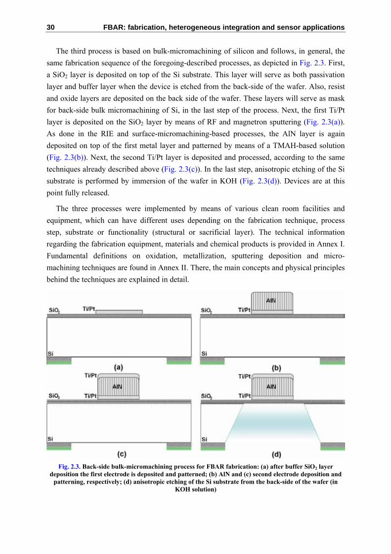
30 FBAR: fabrication, heterogeneous integration and sensor applications
The third process is based on bulk-micromachining of silicon and follows, in general, the same fabrication sequence of the foregoing-described processes, as depicted in Fig. 2.3. First, a SiO2 layer is deposited on top of the Si substrate. This layer will serve as both passivation layer and buffer layer when the device is etched from the back-side of the wafer. Also, resist and oxide layers are deposited on the back side of the wafer. These layers will serve as mask for back-side bulk micromachining of Si, in the last step of the process. Next, the first Ti/Pt layer is deposited on the SiO2 layer by means of RF and magnetron sputtering (Fig. 2.3(a)). As done in the RIE and surface-micromachining-based processes, the AlN layer is again deposited on top of the first metal layer and patterned by means of a TMAH-based solution (Fig. 2.3(b)). Next, the second Ti/Pt layer is deposited and processed, according to the same techniques already described above (Fig. 2.3(c)). In the last step, anisotropic etching of the Si substrate is performed by immersion of the wafer in KOH (Fig. 2.3(d)). Devices are at this point fully released.
The three processes were implemented by means of various clean room facilities and equipment, which can have different uses depending on the fabrication technique, process step, substrate or functionality (structural or sacrificial layer). The technical information regarding the fabrication equipment, materials and chemical products is provided in Annex I. Fundamental definitions on oxidation, metallization, sputtering deposition and micro-machining techniques are found in Annex II. There, the main concepts and physical principles behind the techniques are explained in detail.
Fig. 2.3. Back-side bulk-micromachining process for FBAR fabrication: (a) after buffer SiO2 layer
deposition the first electrode is deposited and patterned; (b) AlN and (c) second electrode deposition and patterning, respectively; (d) anisotropic etching of the Si substrate from the back-side of the wafer (in
KOH solution)

Chapter 2. Development of the FBAR fabrication technology 31
2.2 The aluminum nitride (AlN) layer In the previous section, the concepts of sputtering-based AlN deposition were introduced.
Here, the implementation and characterization results of AlN deposition are discussed.
The AlN piezoelectric layer was deposited by means of RF sputtering on top of a Ti/Pt substrate. Different substrates were considered for AlN deposition. After process compatibility and crystallographic analysis, Pt was adopted as substrate layer for AlN and as material for the electrodes of FBAR. Pt provides good crystallographic compatibility with the c-axis orientation of the AlN film (sputtered AlN crystal presents a hexagonal structure, with preferred orientation in the c-axis, also known as the (002) orientation according to the Miller index notation). Although Al exhibits better CMOS compatibility than Pt, the latter offers improved crystallographic quality and grain size of the AlN film. Atomic force microscopy (AFM) and X-ray diffraction (XRD) characterization were carried-out in order to analyze the crystallographic orientation and quality of the AlN grain for both Al and Pt substrates. Different AlN deposition conditions were tested, the sputtering parameters of Table 2.1 being selected for thickness of 1,000 nm. Annealing or multiple-step depositions were not considered for the establishment of the sputtering setup of Table 2.1.
2.2.1 Thickness and profile No layer planarization was performed in any step of the process, including the AlN
deposition. For this reason, low uniformity of the AlN thickness was expected. In order to evaluate the variation of the AlN layer uniformity, the thickness profile was measured by means of a Nanospec system implementing standard spectrographic techniques with angstrom resolution (Nanospec AFT-200 from Nanometrics). The topographic profile of Fig. 2.4 shows how the thickness of the AlN layer changes as a function of the distance of the measured point to the center of the 100-mm wafer (the sputtering conditions were adjusted to the same values of Table 2.1). According to these results, the standard deviation of thickness is of 74nm for the scanned devices, which corresponds to a variation of around 10% (taken a mean value of 853 nm).
Table 2.1. AC/Magnetron sputtering AlN deposition conditions.
Sputtering parameter
Setup value
RF power 1kW
Ar/N2 concentration 50%-50%
Chamber pressure 1×10⁻² mbar
Estimated substrate temperature
250-300 ºC
Deposition rate 6-7 nm/min.

32 FBAR: fabrication, heterogeneous integration and sensor applications
Fig. 2.4 AlN thickness profile measured by means of the Nanospec AFT-200 system (distance is measured
from the center of the wafer).
2.2.2 Roughness and grain size Atomic force microscopy (AFM) was implemented to perform a detailed analysis of the
surface roughness of AlN film. Samples with different substrate configuration were prepared in order to compare the roughness and grain size. Fig. 2.5(a) to Fig. 2.5(c) present statistical analysis results of the surface roughness of AlN films deposited onto Si, Al and Pt bottom electrodes, respectively. The scanning area on the surface of each sample was of 5×5 μm2. For each case, the roughness was measured at root-mean square (RMS) values of 12, 8.7 and 31.9 nm, respectively. These results are a first indicator of the quality of the AlN film, taking into account that higher grain sizes prompts to higher crystallographic quality in the preferred (002) orientation, for a given deposited material [1]. In these examples, the best grain size –and presumably best crystal quality– is obtained for the AlN film deposited on Pt substrate.
Fig. 2.5. AFM analysis of the AlN surface roughness for different substrates: (a) Si; (b) Al; and (c) Pt.
Chapter 2. Development of the FBAR fabrication technology 33
2.2.3 Crystal quality and orientation In order to determine the actual quality of the AlN crystals, x-ray diffraction (XRD)
analysis was initiated in the Pt-deposited AlN sample, by measuring of the full-width-half maximum (FWHM) aperture angle 2θ/ω of the diffraction pattern, for the set of materials expected to be in the tested wafer.
Diffraction occurs as waves interact with a regular structure whose repeat distance is about the same as the wavelength. It happens that X-rays have wavelengths on the order of a few angstroms, the same as typical inter-atomic distances in crystalline solids. That means X-rays can be diffracted from minerals which, by definition, are crystalline and have regularly repeating atomic structures. When certain geometric requirements are met, X-rays scattered from a crystalline solid can constructively interfere, producing a diffracted beam. In 1912, W. L. Bragg recognized a predictable relationship among several factors [2]:
1. The distance between similar atomic planes in a mineral (the inter-atomic spacing) which is called the d-spacing and measure in angstroms.
2. The angle of diffraction which is called the theta angle and measure in degrees. For practical reasons the diffractometer measures an angle twice that of the theta angle. Not surprisingly, we call the measured angle '2-theta' (2θ).
3. The wavelength of the incident X-radiation, symbolized by the Greek letter lambda (λ).
These factors are combined in Bragg’s law:
θλ sin2dn =⋅ (2.1)
For the case of copper, which is the target material of the X-ray radiation, λ=1.54, and n is assumed to be equal to 1.
A diffractometer, a goniometer, and a scintillation counter for measurement of the X-ray intensity, among other setup elements, are used to make a diffraction pattern of the samples. The goniometer is motorized and moves through a range of 2θ angles. Because the scintillation counter is connected to the goniometer we can measure the X-ray intensity at any angle to the specimen. That is how the 2θ angles for Braggs's Law are determined (see Fig. 2.6).

34 FBAR: fabrication, heterogeneous integration and sensor applications
Fig. 2.6. X-ray diffraction measurement: simplified setup including X-ray source, target material, sample
wafer, goniometer and counter.
In Fig. 2.7(a) to Fig. 2.7(d) the 2θ/ω diffraction peak intensity is plotted for different AlN crystal orientations, including the (002), c-axis orientation. The 2θ angles for each orientation are 33.24 (100), 36.12 (002), 37.94 (101), and 59.40 (110) degrees. As observed in Fig. 2.7, the intensity of the (002)-peak is several orders of magnitude more intense than for the (101), (100) and (110) AlN orientations, being the relationship of 40, 48, and 54 dB, respectively. This means that the AlN crystal exhibits a highly orientation in the c-axis.
Fig. 2.7. X-ray diffraction peak intensity: (a) global XRD pattern (biggest peak: (002) AlN). Detail of (b)
(100) AlN (33.24º), (c) (101) AlN (37.94), and (d) (110) AlN (59.40º) peaks.

Chapter 2. Development of the FBAR fabrication technology 35
Assuming a hexagonal crystal structure and that each 2θ−angle peak corresponds to a specific crystal orientation, the network parameters of the AlN crystal can be calculated. Network parameters are the dimensions and distances of the crystal-plane structure in a certain coordinate space. All lattice planes and lattice directions of the crystal are described by a mathematical description known as a Miller Index [3]. This allows the specification, investigation, and discussion of specific planes and directions of a crystal. In the hexagonal lattice system, the direction [hkl] defines a vector direction normal to the surface of a particular plane or facet, where h, k and l are coordinate axes. Referring to lattice’s d-spacing in equation (2.1), the value of each network parameter is given by:
22221⎟⎠⎞
⎜⎝⎛+⎟
⎠⎞
⎜⎝⎛+⎟
⎠⎞
⎜⎝⎛=⎟
⎠⎞
⎜⎝⎛
cl
bk
ah
d (2.2)
Where a, b and c are the corresponding network parameters. In Fig. 2.8(a) the hexagonal structure of the AlN crystal is depicted. According to this geometry and using equations (2.1) and (2.2), the values of a, b, c and d are calculated to be 2.837, 2.941, 4.973 and 2.487 Ǻ, respectively. These results are very close to 3.084, 3.084, 4.948 and 2.474 Ǻ, which are reference values for hexagonal AlN crystals [4]. The SEM image of Fig. 2.8(b) shows the columnar structure of the CNM25-deposited AlN layer. The columnar-crystal orientation is often associated with good piezoelectric properties (adequate poling is also necessary condition).
Additional information concerning the AlN quality can be extracted from the XRD analysis. The Full Width Half Maximum (FWHM) aperture angle is also an important parameter to evaluate the quality of the crystal: the narrower the angle, the higher the orientation in a certain axis. FWHM is measured in relation to reference materials and its aperture angle depends on width dispersion values for the different planes of the crystalline structure (network parameters of crystal). As a rule of thumb, values less than 1 degree are expected for crystalline materials, strongly oriented in a specific axis.
Fig. 2.8. AlN crystal orientation: (a) Hexagonal lattice structure of AlN; (b) SEM image of CNM25-
processed AlN layer
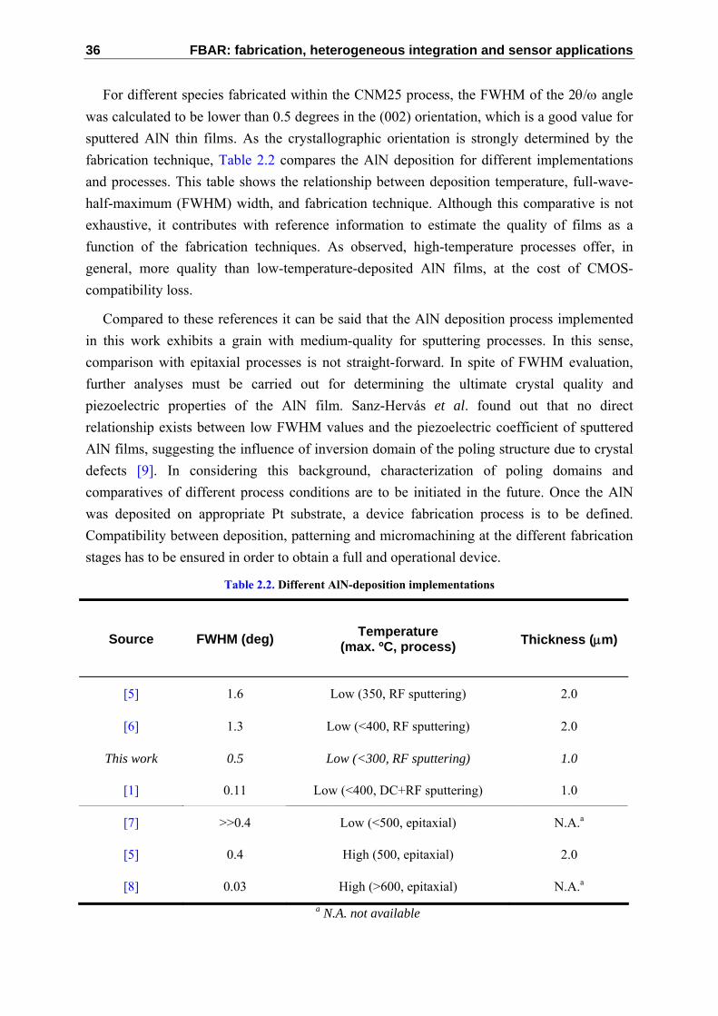
36 FBAR: fabrication, heterogeneous integration and sensor applications
For different species fabricated within the CNM25 process, the FWHM of the 2θ/ω angle was calculated to be lower than 0.5 degrees in the (002) orientation, which is a good value for sputtered AlN thin films. As the crystallographic orientation is strongly determined by the fabrication technique, Table 2.2 compares the AlN deposition for different implementations and processes. This table shows the relationship between deposition temperature, full-wave-half-maximum (FWHM) width, and fabrication technique. Although this comparative is not exhaustive, it contributes with reference information to estimate the quality of films as a function of the fabrication techniques. As observed, high-temperature processes offer, in general, more quality than low-temperature-deposited AlN films, at the cost of CMOS-compatibility loss.
Compared to these references it can be said that the AlN deposition process implemented in this work exhibits a grain with medium-quality for sputtering processes. In this sense, comparison with epitaxial processes is not straight-forward. In spite of FWHM evaluation, further analyses must be carried out for determining the ultimate crystal quality and piezoelectric properties of the AlN film. Sanz-Hervás et al. found out that no direct relationship exists between low FWHM values and the piezoelectric coefficient of sputtered AlN films, suggesting the influence of inversion domain of the poling structure due to crystal defects [9]. In considering this background, characterization of poling domains and comparatives of different process conditions are to be initiated in the future. Once the AlN was deposited on appropriate Pt substrate, a device fabrication process is to be defined. Compatibility between deposition, patterning and micromachining at the different fabrication stages has to be ensured in order to obtain a full and operational device.
Table 2.2. Different AlN-deposition implementations
Source FWHM (deg) Temperature (max. ºC, process) Thickness (μm)
[5] 1.6 Low (350, RF sputtering) 2.0
[6] 1.3 Low (<400, RF sputtering) 2.0
This work 0.5 Low (<300, RF sputtering) 1.0
[1] 0.11 Low (<400, DC+RF sputtering) 1.0
[7] >>0.4 Low (<500, epitaxial) N.A.a
[5] 0.4 High (500, epitaxial) 2.0
[8] 0.03 High (>600, epitaxial) N.A.a a N.A. not available

Chapter 2. Development of the FBAR fabrication technology 37
2.3 Process compatibility Different issues have to be considered in order to achieve compatibility between the
different steps of the FBAR fabrication process:
1. AlN etching with no significant metal electrode etching
2. Metal layer patterning with no co-lateral (undesired) AlN etching
3. Si etching with no significant damage to the FBAR’s structure (bulk micromachining) and Si etching selectivity (against SiO2 and AlN)
4. Sacrificial-layer etching selectivity (surface micromachining)
Different strategies for achieving process compatibility at each one of the foregoing issues have been developed, and are discussed below. To implement these strategies, a group of testing wafers with the FBAR’s composing materials was implemented. These wafers were processed according to the expected process sequence and etchants. Process variations to the sequence and etchants were carried out when the compatibility requirements had demanded it.
2.3.1 AlN etching The AlN layer is patterned by means of wet etching, after immersion of wafers on
determined etchant solutions. Different chemical solutions are commercially available to accomplish this purpose. In considering the Si/SiO2/metal-bottom/AlN/metal-top structure of the FBAR, AlN patterning has to be completed with no damage of the bottom-electrode metal and the SiO2 layers, i.e. the etchant is to be selective to AlN.
In this way, several experiments were carried out, by taking wafer samples with different metal composition and resist configuration, and by etching them with different chemical solutions. The goal of the experiments was to determine which metal-resist configurations were able to survive to etching and which ones were destroyed after immersion in the etchant. Three different commercial etchants were employed: KOH, TMAH and OPD-4262, which is a TMAH-like solution. Metallization made of Al, Ti, Pt, Au, Ni, and combinations of the same were tested. In all the cases, Ti was adhesive metal for Pt, Au, or Ni (candidate substrates for AlN deposition). Also, different etching times were tested on quarter-wafer-sized samples. Table 2.3 shows the results of the AlN compatibility testing. OPD-4262 was selected as etchant solution for AlN with Ti/Pt substrate. This combination ensures reasonable etching times for a 1,000nm-thick AlN layer –between 15-30 min. at etching rates of 500-1,000Ǻ/min– and, at the same time preserves the metallic substrate. Additionally, lateral AlN etching of 1,000-2,000nm is negligible compared to the size of FBAR (tens of micrometers). Etching rates and etch-stop times were determined after visual inspection and profile measurements of the sample.
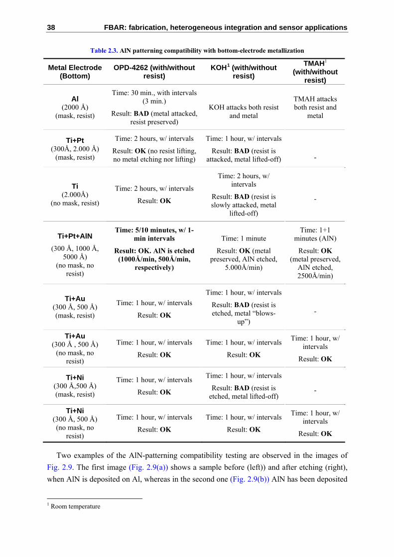
38 FBAR: fabrication, heterogeneous integration and sensor applications
Table 2.3. AlN patterning compatibility with bottom-electrode metallization
Metal Electrode (Bottom)
OPD-4262 (with/without resist)
KOH1 (with/without resist)
TMAH1 (with/without
resist)
Al (2000 Å)
(mask, resist)
Time: 30 min., with intervals (3 min.)
Result: BAD (metal attacked, resist preserved)
KOH attacks both resist
and metal
TMAH attacks both resist and
metal
Ti+Pt (300Å, 2.000 Å)
(mask, resist)
Time: 2 hours, w/ intervals
Result: OK (no resist lifting, no metal etching nor lifting)
Time: 1 hour, w/ intervals
Result: BAD (resist is attacked, metal lifted-off)
-
Ti (2.000Å)
(no mask, resist)
Time: 2 hours, w/ intervals
Result: OK
Time: 2 hours, w/ intervals
Result: BAD (resist is slowly attacked, metal
lifted-off)
-
Ti+Pt+AlN (300 Å, 1000 Å,
5000 Å) (no mask, no
resist)
Time: 5/10 minutes, w/ 1-min intervals
Result: OK. AlN is etched (1000Å/min, 500Å/min,
respectively)
Time: 1 minute
Result: OK (metal preserved, AlN etched,
5.000Å/min)
Time: 1+1 minutes (AlN)
Result: OK (metal preserved,
AlN etched, 2500Å/min)
Ti+Au (300 Å, 500 Å) (mask, resist)
Time: 1 hour, w/ intervals
Result: OK
Time: 1 hour, w/ intervals
Result: BAD (resist is etched, metal “blows-
up”)
-
Ti+Au (300 Å , 500 Å)
(no mask, no resist)
Time: 1 hour, w/ intervals
Result: OK
Time: 1 hour, w/ intervals
Result: OK
Time: 1 hour, w/ intervals
Result: OK
Ti+Ni (300 Å,500 Å) (mask, resist)
Time: 1 hour, w/ intervals
Result: OK
Time: 1 hour, w/ intervals
Result: BAD (resist is etched, metal lifted-off)
-
Ti+Ni (300 Å, 500 Å) (no mask, no
resist)
Time: 1 hour, w/ intervals
Result: OK
Time: 1 hour, w/ intervals
Result: OK
Time: 1 hour, w/ intervals
Result: OK
Two examples of the AlN-patterning compatibility testing are observed in the images of Fig. 2.9. The first image (Fig. 2.9(a)) shows a sample before (left)) and after etching (right), when AlN is deposited on Al, whereas in the second one (Fig. 2.9(b)) AlN has been deposited
1 Room temperature

Chapter 2. Development of the FBAR fabrication technology 39
on Ti/Pt (after etching observed). Both samples were etched with OPD-4262. Although AlN remains in both samples according to the etch-mask, it can be seen how the metallization has disappeared from the first sample (still the underlying Al –in white–, protected by the etched AlN, can be seen). In Fig. 2.9(b) the Ti/Pt layer corresponds to light areas. In both images AlN is the transparent purple area.
2.3.2 Metal layer patterning From previous AlN-patterning testing, Al was discarded as suitable metal layer (regarding
OPD-4262 patterning and AFM analysis). Thus, metal-layer patterning analysis was performed on Pt, Au and Ni metallization (all of them implementing Ti as adhesive layer). These metals were patterned by means of lift-off after immersion of samples in acetone. Additional ultrasound shaking further increased the efficiency of the resist removal. Table 2.4 shows how the Ti/Pt combination achieved the best lift-off results with no damage of previous layers (including AlN for the FBAR’s top-electrode patterning).
2.3.3 Front-side reactive-ion-etching (RIE) of silicon Once the structural layers of the FBAR have been deposited and patterned, the last but
most critical step of dry etching is to be initiated. In this process, Si is etched by means of RIE. This process entails several compatibility challenges to the process, mainly due to selectivity with respect to other materials in the FBAR’s structure, especiallly to SiO2 and AlN.
The size of devices and the etching rate is the first issue to be considered. Since some anisotropy is found in RIE, vertical and lateral etching rate have to be measured. The etching-stop time is a manufacturing decision based on the lateral size of devices in the wafer. Also, RIE selectivity to other materials and size of devices can affect or mask the etching-rate measurements.
Fig. 2.9. AlN compatibility testing results: (a) AlN deposited on Al, before (left) and after (right) wet etching with OPD-4262 (the Al layer in white has disappeared after etching, insight down). (b) AlN
deposited on Ti/Pt (the metal remains on the wafer after AlN etching, insight down)

40 FBAR: fabrication, heterogeneous integration and sensor applications
Table 2.4. Compatibility testing for metal-layer patterning
Metal Electrode (Bottom) Lift-off
(only wafers with resist, acetone)
Ti+Pt (300Å, 2.000 Å)
(mask, resist)
Time: 10 minutes
Result: OK
Ti+Au (300 Å, 500 Å) (mask, resist)
Time: 10 minutes
Result: FAIR-POOR. Resist lifted-off for small patterns (max. 50%), and for bigger
ones (~50%)
Ti+Ni (300 Å,500 Å) (mask, resist)
Time: 10 minutes, w/ intervals
Result: BAD (metal did not lift-off)
In our particular case, the width of pattern sizes for deciding the etching-stop time was defined to be 50-100 μm. SEM, Nanospec profile-meter and visual inspection of wafers were employed to evaluate vertical and lateral etching rates. The SEM images of Fig. 2.10(a) and Fig. 2.10(b) shows cross-sectional-view of sample profiles after RIE. Etching-windows were opened in a protective, metallic layer deposited on top of the Si layer. Looking into Fig. 2.10(a), the lateral versus vertical etching rate can be estimated to be between 1:3 and 1:4. In this case, the vertical etching is around 100 μm, whereas the lateral under-etching is around 30-35 μm. Lateral-etching rate was calculated to be 1,500–1,600 Å/min. On the other hand, the small-windowed structure of Fig. 2.10(b) reveals a lower lateral-to-vertical aspect ratio, the same being in the order of 1:2. However, the etching rate was also reduced for this case. Thus, it was found that the size of the window influences not only the aspect ratio but also the etching rate. In such a way, the size of devices and etching-windows should be carefully designed in order to find the best combination: small-windows make more efficient the layout design, but reduce the etching-rate, so as bigger windows increase the etching-rate at the cost of bigger under-etching areas. According to calculated lateral-etching areas, releasing of a 50μm-wide device would require a minimum etching time of around 3 hours.

Chapter 2. Development of the FBAR fabrication technology 41
Fig. 2.10. RIE profile and etching rate evaluation (SEM images)
A second topic important for developing the etching technology is the RIE selectivity. Although extensive testing demonstrated that no significant etching of AlN or metal layers occurred for long exposures to etching plasma, the SiO2 suffered from important etching. This means that for typical etching times of around 3-4 hours, the SiO2 layer disappeared before the complete release of a 50μm device. Actually, the etching rate was estimated to be of 250-350 Ǻ/min, which leads to complete etching of a 8,000 Ǻ-thick SiO2 layer in about 25-30 min. Since the metal electrodes of FBAR are deposited on top of the SiO2 layer, high under-etching of Si leads to instability of the oxide and metal layers. Also, the SiO2 passivation functionality is lost due to full etching of it along the non-covered areas. The SEM image of Fig. 2.11(a) shows the aspect of metal layer after RIE. Due to lateral under-etching of both the Si substrate and the SiO2 layer, the metal layer (in light) loses its support, and begins to bend and release from the substrate (the grey areas are “flying” metal with no SiO2 support). In Fig. 2.11(b) the upper-view confocal image of the same structure is observed. Here, the (clear) areas in gold are metal, the rough regions in blue are etched Si, and the dark, black areas bordering the gold (clear) are also bent metal with no underlying SiO2. Longer etching times lead to complete destruction of the electrode structure.
Fig. 2.11. Silicon dioxide under-etching: (a) SEM image of test structure showing the effects of RIE on the metal structure (gray areas are bent metal). (b) Confocal image of the same structure (the black borders
correspond to bent metal areas)

42 FBAR: fabrication, heterogeneous integration and sensor applications
There are two ways for reaching compatibility of RIE with SiO2 layer. The trivial one, but not feasible, is to reduce the etching time of Si. The second option is to protect the wafer with a material selective to the Si etching’s recipe, which can be Al, for example. If such a protective layer can be deposited, still providing an etching-window to etch the Si substrate, processing can take an arbitrary time (from the point of view of SiO2 selectivity).
Thus, using the same mask of the etching-window, a protective Al/Cu layer was deposited and patterned in order to cover the whole front-side surface of the wafer (exception for the areas in which Si is to be etched). Fig. 2.12 shows sample FBARs and co-planar test structures with the Al/Cu cushion (light region) covering the ensemble. The dark area around the device is the Si substrate looked through the etching-window. The corrugated region around the window is the under-etched SiO2 area (no underlying Si is supporting the device’s structure, so a SiO2 membrane is created around the device).
Once finished the RIE, the Al/Cu cushion is removed by means of a wet-etching process, in order to provide a fully released device. At this stage, the fabrication process is finished and the device can be characterized. The optical images of Fig. 2.13 show full FBARs at the end of the process. The under-etched area underneath the SiO2 is observed in purple. Some traces of the Al/Cu still remain on this region, close to the etching-window. The light area is the Ti/Pt metallization, the green area is SiO2 on Si, and the AlN layer is the purple, transparent rectangular region in the center of the image. The detailed, step-by-step description of this process can be found in Annex III (“Front-side, reactive-ion-etching-based process for FBAR fabrication”).
Fig. 2.12. Al/Cu cushion covering rectangular (a) and rhomboidal (b) FBAR devices for SiO2 protection
during RIE

Chapter 2. Development of the FBAR fabrication technology 43
Fig. 2.13. Fully-released FBARs after Al/Cu cushion removing.
2.3.4 Surface micromachining of a sacrificial layer A second process based on surface-micromachining of a Ti sacrificial layer was
implemented. This approach has the main advantage to be much faster than RIE-based processes. In this implementation, the Ti sacrificial layer is etched using HF with a concentration of 49%. Because the bottom electrode is in contact with the sacrificial layer, Cr replaces Ti as the adhesive layer for Pt, which is used to fabricate both bottom and top electrodes of the resonator (otherwise the bottom electrode would lift-off due to etching of the adhesive layer). Typical etching times for a 50 μm-sized structure are 5–10 minutes, leading to an etching rate in the order of 35,000–70,000 Å/min, which is more than 40 times the estimated rate for dry-etching (RIE). Cross-sectional view of the process before sacrificial layer etching is shown in Fig. 2.14. As observed in the illustration, a SiO2 layer is deposited on top of Si. After this layer, a passivation layer is now made of Si3N4, which is patterned to open a window to the Ti sacrificial layer. Also, the SiO2 layer is partially attacked during wet etching, and is deposited to alleviate the sacrificial-layer thickness requirements.
Fig. 2.14. Surface micromachining process before etching of the sacrificial layer

44 FBAR: fabrication, heterogeneous integration and sensor applications
Selectivity and compatibility testing of the different layers was performed prior to final-device fabrication. Evaluation of etching rates and integrity of the device were the main goal of this testing. For this purpose a set of test wafers with different layer configurations were prepared. Hence, the etching rates for Ti, Cr, SiO2 and Si3N4 were measured. With this information, the etching times were adjusted to obtain a released device with minimum damage and the shortest processing times. On the other hand, since AlN and Pt are highly selective to HF, they did not suffer from significant damage during testing.
First, the selectivity of Cr to HF etching and the etching rate of Ti were evaluated. A test wafer with Si/Ti/Cr configuration, and etching-mask providing etch-windows in the Cr layer was prepared (Ti and Cr thicknesses of 1,000 and 400nm, respectively). In this way, HF penetrated through the holes in the Cr layer to etch the underlying Ti layer. Fig. 2.15(a) shows the mask layout with openings in light color, whereas Fig. 2.15(b) shows a detailed view of the mask with pattern and under-etching dimensions after 12 min. of etching. Thus, for this specimen, the Ti etching rate is calculated to be of 40,000 Å/min. No change in the dimensions or shape of the Cr layer was observed. However, slight differences in the Ti etching rate were observed when measuring the size of different patterns. In considering the window-size factor and after several measurements, the etching rate range was determined to be of 35,000–70,000 Å/min.
Once the integrity of Cr was verified, the SiO2 etching rate was measured. Therefore, a second wafer with Si/SiO2/Cr layer configuration and the same etch-mask used in the previous experiment was prepared. The thicknesses of SiO2 and Cr are 1,000 and 200nm, respectively. In this case and for a 9-min. etching time, the under-etched area underneath the Cr augmented, obtaining an etching rate of around 120,000 Å/min, as observed in Fig. 2.16(a) and Fig. 2.16(b). This rate is more than twice the etching rate value found for Ti.
Fig. 2.15. Ti/Cr etching-selectivity testing: (a) sample with Si/Ti/Cr configuration (opening windows in
light color showing underlying Ti layer); (b) detailed view of the etch window with under-etching observed underneath the Cr layer.

Chapter 2. Development of the FBAR fabrication technology 45
Fig. 2.16. SiO2/Cr etching-selectivity testing: (a) sample with Si/ SiO2/Cr configuration (opening windows
in light color showing underlying SiO2 layer); (b) detailed view of the etch window with under-etching observed underneath the Cr layer.
In this testing, the etching times were selected in considering the final-device dimensions –width of 50-100μm–. According to these results and to the FBAR process layout depicted in Fig. 2.14, and considering the FBAR size and same or similar thicknesses for the Ti and SiO2 layers, an air-gap resulting from total etching of the sacrificial Ti layer and partial etching of the buffer SiO2 layer is expected. In Fig. 2.17 a completely-released FBAR device is observed. The light-gray area around the device is Si, after Ti and SiO2 etching. The dark-gray area is the passivation Si3N4 layer. The detailed, step-by-step description of this process can be found in Annex IV (“Surface-micromachining-based process for FBAR fabrication”).
2.3.5 Back-side bulk micromachining of silicon (wet etching) The last etching process studied in this work is based on bulk micro-machining of Si,
which has been used for long time in fabricating FBARs. This process has the advantage to be auto-controlled, in the sense that the etching stops when reaching a specific angle in the crystallographic structure of Si. This advantage can be exploited if a proper mask is designed to make the desired pattern size being coincident with the stopping angle.
Fig. 2.17. Surface-micromachined FBAR device after wet-etching of the sacrificial layer: (a) Illustration of
the cross-sectional layout; (b) Optical microscope image (up view)

46 FBAR: fabrication, heterogeneous integration and sensor applications
On the other hand, this feature is independent of the disparity in size for different devices on the same wafer, the thickness of the wafer and the etching rate being the main control parameters. In this approach the front-side RIE mask has to be replaced by the back-side mask to perform the wet etching. The bulk micro-machined FBAR implementation of this work is represented in the schematic drawing of Fig. 2.18. The SiO2 layer has a thickness of 4,000 Ǻ and serves as protective means for the structural layers of the FBAR, thus preventing further etching of its composing materials. The metal electrodes are made of Ti/Pt and have the same thickness of previous processes. The wet-etching is performed by submersion of the wafer in a buffered KOH solution.
Structural testing was performed after deposition and patterning of each layer. According to the layout of Fig. 2.18, test wafers were fabricated. First, the bottom electrode processing was carried out. The front-side and back-side of the wafer after deposition of the first metal layer and Si etching are observed in Fig. 2.19(a) and Fig. 2.19(b), respectively. Here, the square-shaped membrane appears in light color around the rounded metal electrode (lightest color, center). No appreciable stress or membrane fractures are evident after this testing.
Different situation is found when additional layers are deposited. The accumulated stress on subsequent layers is thus transmitted to the SiO2 membrane. After AlN deposition, the first membrane fractures and metal bending began to be evident, as shown in Fig. 2.20. With the aim of improvement of the fabrication yield, careful measurement of the etching time was carried out in order to avoid excessive etching times. Although successful fabrication of complete devices was accomplished, electrical characterization and visual inspection demonstrated a low fabrication-yield. The detailed, step-by-step description of this process can be found in Annex V (“Back-side, bulk-micromachining process for FBAR fabrication”).
Fig. 2.18. Cross-sectional view schematics of the bulk micromachining FBAR process

Chapter 2. Development of the FBAR fabrication technology 47
Fig. 2.19. Structural testing after first metal deposition: (a) front-side, and (b) back-side of the wafer. The
light-color squared area around the central device is the SiO2 membrane on top of the cavity, after Si under-etching.
Fig. 2.20. Structural testing after AlN deposition: (a) front-side, and (b) back-side of the wafer. The first
fractures in the SiO2 membrane begin to be evident.
The main technology development aspects have been discussed in previous sections. As commented above, the detailed, step-by-step descriptions of each process can be found in Annex III (RIE-based process), Annex IV (surface micromachining process) and Annex V (back-side, bulk micromachining process).
2.4 Structure analysis In this section, the device structure is analyzed. Scanning-electron-microscopy,
interferometer and confocal microscopy techniques have been implemented to study the structural composition and process results of the fabricated FBAR devices.
2.4.1 Scanning-electron-microscopy (SEM) analysis SEM has been one of the main characterization tools implemented in this work for
supervision of the FBAR’s structure. Based on several inspection and measurements, the overall device structure and the details of each layer were analyzed. In previous sections, some SEM images illustrated the results of AlN deposition and technology compatibility. In this section we will focus on analyzing the final-device FBAR’s layer configuration.

48 FBAR: fabrication, heterogeneous integration and sensor applications
The layout of a complete device comprising top and bottom electrodes, AlN and passivation layer is observed in the SEM image of Fig. 2.21(a). Under the etch-window (dark region) the Si substrate is found. Appropriate processing of the layer structure of the FBAR allows the evaluation of the quality and thickness of each layer in the FBAR’s stack. In Fig. 2.21(b) the layout configuration of a focused-ion-beam-milled FBAR is shown. The metal-AlN-metal sequence is observed. Applying a correction factor of the vertical scale –due to the set-up tilting of the electron-beam– the thickness of the composing materials can be measured (given the topographic scale, annotated in the image). In this example, tilting angle is 52º, the metal-AlN-metal layers having thicknesses of 180nm, 1,000nm and 180nm, respectively. Also, the air cavity underneath the structure is observed. In partially-released devices some Si still remains underneath the bottom electrode, as seen in Fig. 2.21(c). In this case, further processing by longer RIE times is required to finish the FBAR fabrication.
2.4.2 Interferometer analysis Interferometer analysis is also a useful technique to evaluate the structure of fabricated
devices. Specifically, stress levels and etching-releasing of device can be studied from the interferometer images. In Fig. 2.22(a) and Fig. 2.22(b) we can see interferometer images of two different devices and the effects of fabrication and etching on their structure.
Fig. 2.21. FBAR structure after fabrication: (a) Overall layout; (b) Insight into the layered metal-AlN-
metal structure (tilting angle of 52º, thicknesses of Pt, AlN and AlN of 180, 1,000 and 180nm, respectively); and (c) Partially-released device (Si substrate is still observed underneath the device)

Chapter 2. Development of the FBAR fabrication technology 49
Fig. 2.22. Interferometer analysis of the FBAR structure: (a) partially-released, cantilever-type device
(partial bending and non-homogeneous interferometer bands are observed); (b) fully-released, beam-type resonator (homogeneous bands and topographic levels all along the device)
First, a partially-released cantilever is shown in Fig. 2.22(a), where interferometer bands (down) are observed only in the released region of the device (area near the border of the electrode). This observation is corroborated with the topographic image (up), where bending of the device due to residual stress can be deduced from the higher-scale levels near the border of the device (red to yellow). The central region in blue is still clamped to the Si substrate.
On the other hand, the FBAR of Fig. 2.22(b) exhibits relatively-homogeneous scale levels (up) and interferometer bands (down). In this case, the square-shaped, beam-type device has been fully released from the substrate, thus vibrating at its natural mechanical frequency (MHz) all along its structure. However, considerable stress in the beam can be observed, when contrasting the topographic levels at the center and lateral regions, where one of the clamped electrodes is found (at left). Both devices –cantilever and beam– were fabricated according to the RIE-based process.
2.4.3 Confocal microscopy Confocal microscopy allows getting additional details on the structure of certain processes,
specifically for thin-film devices like FBAR [10-11]. Typically, flatness, stress, or sticking of the structure can be analyzed. Also, the etching status of a micromachining process can be supervised. In Fig. 2.23(a) the conformation of FBAR with co-planar structure is shown. From this confocal image we can evaluate the dimensions of big layer-steps and the integrity of the device, especially for very thin layers like the Ti/Pt metal electrodes. Increasing or reducing of the thickness of said layers can be decided according to this analysis. In this case, the top electrode in yellow –180nm– is a higher-topographic layer, due to its deposition on top of the AlN (1,000nm). No discontinuity is observed near the FBAR-to-pad interface (Fig. 2.23(b)), or in the central region of the resonator (Fig. 2.23(c)).

50 FBAR: fabrication, heterogeneous integration and sensor applications
Fig. 2.23. Confocal microscope images for FBAR fabrication monitoring: (a) Overview of FBAR with co-planar testing structure; (b) FBAR-to-testing pad interface detailing the top electrode step (top electrode
in yellow); and (c) Central region of the device, detailing the resonator.
After micromachining, the structure or the contour regions of the device may suffer from damage or deformation due to residual stress after releasing. In Fig. 2.24 two devices fabricated within RIE and surface micromachining processes are compared. In Fig. 2.24(a), accumulated stress in the SiO2 membrane is observed around the region with no underlying Si (in blue, after Si under-etching). Such stress is evidenced as deformation and, in some parts, cracking of the membrane (around the etch-window in black). The situation of a surface-micro-machined device is rather different, as shown in the confocal image of Fig. 2.24(b). First, lower processing times and less fabrication steps alleviate induced stress. Roughly, a relatively flat structure is achieved, if compared to that obtained by the first process. The top electrode’s step is depicted in red (along the rose-colored path). A quasi-flat topographic profile of the same device along the A-A’ axis can be seen in Fig. 2.24(c). According to previous description of the surface-micromachining-based process, the 1.5μm-thick sacrificial layer has already disappeared. The top electrode and the overall FBAR structure have also an almost-flat conformation.

Chapter 2. Development of the FBAR fabrication technology 51
Fig. 2.24. Stress and flatness confocal-supervision: (a) RIE-based FBAR (accumulated stress in the SiO2 membrane is observed); (b) Surface-micromachined FBAR (sacrificial-layer cavity after etching in dark
blue); and (c) Topographic profile of the device (along the A-A’ axis)
2.5 Summary The FBAR technology has been developed within the CNM25 process. Three different
micro-machining processes have been designed and FBARs fabricated. Different characterization techniques have been implemented in order to evaluate the main steps of the process. Also, the complete, layered FBAR structure has been studied using SEM, interferometer and confocal microscopy. Although a variety of parameters should be considered, Table 2.5 attempts to compare the different aspects concerning FBAR-related micro-machining. Advantages and challenges of each technology should be sought in considering the possibilities and limitations of the technology available to the designer. In our case, the process based on front-side micro-machining of silicon represents a good trade-off between quality of final devices and fabrication parameters. Hence, in the following chapters, this thesis deals with the performance and applications of FBAR, in considering the RIE-based implementation.

52 FBAR: fabrication, heterogeneous integration and sensor applications
Table 2.5. Micromachining implementations in the fabrication of FBAR
Fabrication issue
RIE of Si (Front-side bulk micromachining)
Ti sacrificial layer(Surface
micromachining)
KOH etching of Si (Back-side bulk
micromachining)
Design complexity
4-mask set, including RIE mask
4-mask set, including sacrificial
layer mask
5-mask set, including additional back-etching mask
Fabrication complexity
High metal step (top and bottom)
Sticking, critical etch. time (to avoid
metal lift-off)
Front-to-back mask alignment, residual silicon on back side
Etching rate 1,500 Å/min >35,000 Å/min ~3,300 Å/min
Etching time (50μm × 50μm, wafer: 500 μm)
240 min. 5-10 min. 1,500 min. (~ 24 h.)
Cleanness More clean Less clean Less clean
Residual stress Medium Low High
Etching control Time-supervised Time-supervised Self-controlled
Wafer area required
Under-etching of non-FBAR regions Less than RIE More than RIE
Quality Factor High (>700) Low (<100) Low (<100)
References 1 M. Clement, L. Vergara, J. Olivares, E. Iborra, J. Sangrador, A. Sanz-Hervás, Z. Zinck, “SAW and
BAW response of c-axis AlN thin films sputtered on platinum”, in Proc. IEEE Intl. Ultrason. Symp. 2004, Aug. 24-27 2004, Montreal, Canada, 1367-1370.
2 M. F. Perutz, “How W. L. Bragg invented X-ray analysis”, Acta Cryst. A 46 (1990) 633-643.
3 Neil W. Ashcroft and N. David Mermin, Solid State Physics (Harcourt: New York, 1976).
4 A.F. Wright, and J.S. Nelson, “Consistent structural properties for AlN, GaN, and InN”, Phys. Rev. B: Condens. Matter 51 (1995) 7866-7869.
5 F. Engelmark, G.F. Iriarte, I.V. Katardjiev, M. Ottosson, P. Muralt, and S. Berg, “Structural and electroacoustical studies of AlN thin films during low temperature radio frequency sputtering deposition”, J. Vac. Sci. Technol. A 19 (2001) 2664-2669.
6 M. Hara, J. Kuypers, T. Abe, and M. Esashi, “Surface micromachined AlN thin film 2 GHz resonator for CMOS integration”, Sens. Actuator A-Phys. 117 (2005) 211-216.
7 T. Shiosaki, T. Yamamoto, T. Oda, K. Harada, and A. Kawabata, “Low temperature growth of piezoelectric films by RF reactive planar magnetron sputtering”, Jap. J. Appl. Phys. 20 (1981) 149-152.
8 S. Uchiyama, Y. Ishigami, M. Ohta, M. Niigaki, H. Kan, Y. Nakanishi, and T. Yamaguchi, “Growth of AlN films by magnetron sputtering”, J. Crystal Growth 189-190 (1998), 448-451.

Chapter 2. Development of the FBAR fabrication technology 53
9 A. Sanz-Hervás, M. Clement, E. Iborra, L. Vergara, J. Olivares, and J. Sangrador, “Degradation of the piezoelectric response of sputtered c-axis AlN thin films with traces of non-(0002) x-ray diffraction peaks”, Appl. Phys. Lett. 88 (2006) 161915.
10 D. Semwogerere and E.R. Weeks, “Confocal Microscopy”, published in the Encyclopedia of Biomaterials and Biomedical Engineering, Taylor & Francis (2005).
11 V. Prasad, D. Semwogerere, and E.R. Weeks, “Confocal microscopy of colloids”, J. Phys.: Cond. Mat. 19 (2007) 113102.

CHAPTER 3
FBAR devices: characterization and modeling
Characterization and modeling of FBARs comprise different methods and techniques, and are performed through successive measurement stages. Material and equivalent-circuit parameter extractions enable for a complete description of the device, which can be used to design specific FBAR-based applications. On the other hand, since frequency and temperature stability are also required to achieve competitive performance of the resonator in sensor and RF applications, further characterization and design optimization is required.
In section 3.1 different measurement setups are described and the main concepts behind S-parameter characterization are presented. The main devices designed and fabricated in the context of this thesis, are also presented in section 3.2. The equivalent-circuit-parameter model of FBARs is introduced in section 3.3, for the particular case of our process, thus including parasitic and substrate-related circuit elements. Two characterization approaches based on S-parameter analysis are discussed. In the first one, the low-frequency measurement results are presented in section 3.4, thus discussing the mechanical and electrical parameter extraction, the fundamental resonance modes, and other properties of FBARs as micro-mechanical structures. In the second one, high-frequency analysis of each device is detailed in section 3.5. The quality factor, the electro-mechanical coupling and the piezoelectric constants of AlN are discussed along this section. In section 3.6 an algorithm for the automated extraction of equivalent-circuit parameters is described. Some applications of this tool are also proposed in this section.
After ‘ideal-device’ characterization, process deviations and stability issues are studied in section 3.7, including time stability and thermal coefficients evaluation.. Next, in section 3.8 a temperature-compensated implementation and the corresponding characterization results are presented. Post-fabrication tuning of the FBAR’s resonance frequency is studied in section 3.9. Thus, a novel, low-impact tuning technique based on focused-ion-beam is introduced in this section. The complete list of instrumentation and resources utilized for device characterization is provided in Annex VI.
3.1 Scattering parameters and characterization setup Transmission and reflection measurements are the best way to describe the electrical
response of FBAR devices working in the GHz frequencies. In particular, the scattering-parameter representation –or S-parameters– is very useful to explain the impedance and energy relationships of the RF system comprised by an FBAR, the transmission line

56 FBAR: fabrication, heterogeneous integration and sensor applications
connecting said device to the measurement system, and the probing pads at which the test instrumentation is connected to the circuit. S-parameters are used to evaluate microwave circuits and come from the two-port circuit representation shown in Fig. 3.1, where two sets of ingoing (ai) and outgoing (bi) waves are generated. The indices i = 1, 2 stand for the input and output port, respectively.
Fig. 3.1. Two-port circuit representation with scattering parameters
These four quantities are related together by the scattering matrix S:
⎥⎦
⎤⎢⎣
⎡⎥⎦
⎤⎢⎣
⎡=⎥
⎦
⎤⎢⎣
⎡
2
1
2221
1211
2
1
aa
SSSS
bb
(3.1)
The individual S-parameters are found by setting one of the independent variables to zero:
01
111 2== aa
bS
02
112 1== aa
bS (3.2)
01
221 2 == aa
bS
02
222 1== aa
bS
Each parameter is thus defined as [1]:
• S11: Reflection coefficient at port-1 when port-2 is terminated with a matched load (S11 is related to the input impedance)
• S12: Reverse transmission coefficient when port-1 is terminated with a matched load • S21: Forward transmission coefficient when port-2 is terminated with a matched load • S22: Reflection coefficient at port-2 when port-1 is terminated with a matched load
(S22 is related to the output impedance)
Typically, the transmission line can be a co-planar waveguide (CPW), which we do actually implement in our systems to connect FBARs to the measurement system. In this way, the S-parameters can also be defined in terms of the circuit and CPW electrical characteristics [2]:
( )( )LZZZS
inS
in
λ++=
1211 (3.3)
( )( )LZZZSinS
S
λ++=
122
21
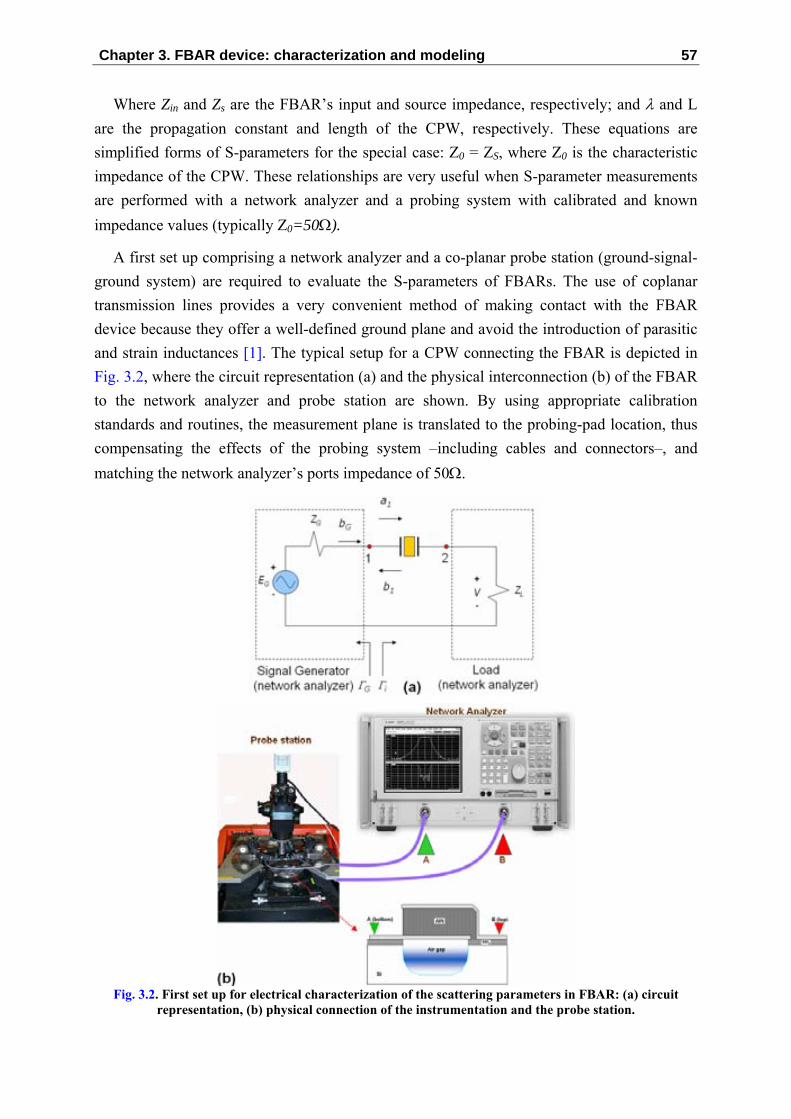
Chapter 3. FBAR device: characterization and modeling 57
Where Zin and Zs are the FBAR’s input and source impedance, respectively; and λ and L are the propagation constant and length of the CPW, respectively. These equations are simplified forms of S-parameters for the special case: Z0 = ZS, where Z0 is the characteristic impedance of the CPW. These relationships are very useful when S-parameter measurements are performed with a network analyzer and a probing system with calibrated and known impedance values (typically Z0=50Ω).
A first set up comprising a network analyzer and a co-planar probe station (ground-signal-ground system) are required to evaluate the S-parameters of FBARs. The use of coplanar transmission lines provides a very convenient method of making contact with the FBAR device because they offer a well-defined ground plane and avoid the introduction of parasitic and strain inductances [1]. The typical setup for a CPW connecting the FBAR is depicted in Fig. 3.2, where the circuit representation (a) and the physical interconnection (b) of the FBAR to the network analyzer and probe station are shown. By using appropriate calibration standards and routines, the measurement plane is translated to the probing-pad location, thus compensating the effects of the probing system –including cables and connectors–, and matching the network analyzer’s ports impedance of 50Ω.
Fig. 3.2. First set up for electrical characterization of the scattering parameters in FBAR: (a) circuit
representation, (b) physical connection of the instrumentation and the probe station.

58 FBAR: fabrication, heterogeneous integration and sensor applications
The calibration standards used in this setup are coplanar TOSL structures fabricated on printed-circuit substrates provided by Cascade. The name TOSL stands for Thru, Open, Short, and Load (50Ω in our case). These are the standards traditionally used with an automatic network analyzer and are suitable for calibration routines limited to coaxial transmission lines in the frequency range from DC to 6 GHz. To perform the calibration, the standard kit implements two components: the printed-circuit TOSL substrate and the standard software, against the measurements are compared during calibration.
In a second set up, a printed circuit board (PCB) replaces the co-planar probe station. In this PCB a CPW is designed in order to connect the FBAR die to the measurement instrumentation. The FBAR die is attached to the PCB and connected to the PCB-made transmission lines by means of wire-bonding. For this purpose, the PCB’s CPW design has to guarantee impedance matching to the 50Ω value of the port impedance of the network analyzer (appropriate PCB design and careful selection and knowledge of the dielectric constants of the PCB’s laminate are required). The circuit representation of this setup is the same already depicted in Fig. 3.2(a). A schematic representation of an exemplary PCB-FBAR system is depicted in Fig. 3.3(a), and the physical set up comprising the PCB and the network analyzer is shown in Fig. 3.3(b). The calibration standards used in this setup are co-planar TOSL structures implemented as coaxial connectors fabricated by Agilent Technologies.
Fig. 3.3. Second set up for electrical characterization in FBAR: (a) schematic representation of the PCB-
FBAR system, (b) physical interconnection of the PCB and the network analyzer.

Chapter 3. FBAR device: characterization and modeling 59
The PCBs were fabricated using laminates made of the high-frequency dielectric material Rogers 3010®, which is a ceramic-filled PTFE composite with low dielectric loss and application up to 10GHz [3]. The network analyzer Agilent E5100A was employed in both measurement systems; whereas a MicroTec probe station (Süss) and a custom-designed PCB were used in the co-planar-probe set up and in the packaged-system set up, respectively. A complete list of the measurement instrumentation and calibration kits is provided in Annex VI.
3.2 Device description In chapter 2 the FBAR’s fabrication technology and processes were described. According
to these processes, devices with layout variety were designed and fabricated, all the devices being suitable for fabrication upon the three micromachining technologies already presented. In this section, we explain the particularities of the main FBAR geometries that have been implemented in this work.
3.2.1 Type I: The irregular rhomboid device The irregular rhomboid device is a tetragon-shaped FBAR having different dimensions for
each one of its sides and no parallelism between them. This design has been intended for lateral-mode resonance suppression, said type of layout being referred to as the apodized resonator by some authors [4]. Irregular rhomboid devices have dimensions of 150×130 μm2, and different versions, including a through-hole version, were implemented. RIE-based, surface and back-side bulk micro-machined implementations of the irregular rhomboid device were fabricated. The layout and dimensions of this kind of FBARs are drawn in the top-view schematic of Fig. 3.4(a). A realization of said device is observed in the SEM image of Fig. 3.4(b). As it will be analyzed later, this device exhibits reduced lateral-mode resonances and the best insertion-loss and quality-factor performance among all the FBARs implemented by our group.
Fig. 3.4. Irregular rhomboid FBAR (type I): (a) schematic view; (b) “classical” device with no holes
(SEM); (c) modification with reduced AlN borders (SEM); (d) through-hole version (SEM)

60 FBAR: fabrication, heterogeneous integration and sensor applications
However, due to its size, the time required for releasing its structure is among the highest of the designed devices, being over 6 hours for the RIE-based process.
3.2.2 Type II: The decagon device with holes (“The Orange”) The decagon device with holes is a decagon-shaped FBAR having been designed in two
different versions of the same size (the difference is the layout of the through-holing of the structure). Again, the main idea of this design was to reduce the lateral-mode resonances. The through-hole version of this device is intended for etching-time reduction and due to its layout we refer to it as the Orange FBAR. Surface and front-side RIE-micro-machined devices were fabricated and characterized. The layout and 130μm-sided dimensions of this kind of FBARs are drawn in the top-view schematic of Fig. 3.5(a). Different realizations of said device are observed in the optical and SEM images of Fig. 3.5(b) to Fig. 3.5(d).
This device also exhibits reduced lateral-mode resonances and good insertion-loss and quality-factor performance. However, its structure demonstrated to be fragile to processing and susceptible to bending, surely due to inadequate stress-loading distribution along its geometry.
Fig. 3.5. Decagon FBAR with holes – The Orange (type II): (a) schematic view; (b) round-shaped holes
version (optical); (c) top view of the device, “wheel-shaped” holes (optical) and (d) bird’s eye view of the “wheel-shaped”-hole device (SEM)

Chapter 3. FBAR device: characterization and modeling 61
3.2.3 Type III: The decagon device with no holes The decagon device without holes is a decagon-shaped FBAR having the same layout and
purposes of the Orange resonator, the only difference with the former being the absence of through-holing. Again, the main idea of this design was to reduce the lateral-mode resonances. However, the absence of through-holes increased the etching time, compared to the through-holed Orange FBAR. Devices fabricated according to the three micromachining processes described in chapter 2 were characterized. The layout and dimensions of this kind of FBARs are the same of the through-holed device and are drawn in the top-view schematic of Fig. 3.6(a). A realization of said device is observed in the optical image of Fig. 3.6(b).
Fig. 3.6. Decagon FBAR with no holes (type III): (a) schematic view; (b) “classical” device with no holes
(optical)
This device also exhibits reduced lateral-mode resonances and, compared to the Orange, better insertion-loss and quality-factor performance. This is due to its increased electrode area, which is the difference between the holed and non-holed regions of this device and that of the type II. However, its structure also demonstrated to be fragile to processing, surely due to inadequate stress-loading distribution along its geometry.
3.2.4 Type IV: The round-shaped device The round-shaped FBAR has a geometry intended for lateral-mode resonance reduction.
Two versions of this device were designed: the small one and the big one, the difference being the radius of the circle limiting the electrode’s area (50μm and 75 μm for the small and big, respectively). Front-side RIE and back-side bulk micromachining processes were implemented in the fabrication of round FBAR devices. The layout and dimensions of this kind of FBARs are drawn in the top-view schematic of Fig. 3.7(a). A realization of said device is observed in the optical image of Fig. 3.7(b).
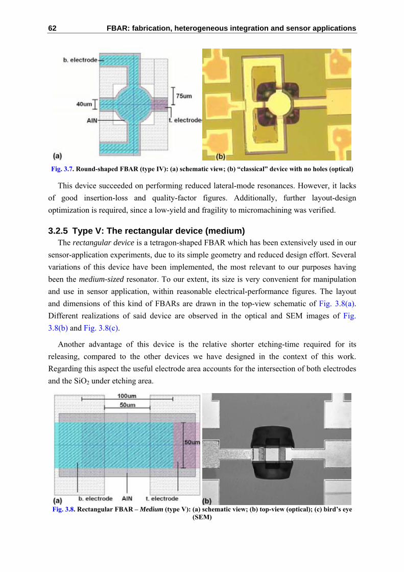
62 FBAR: fabrication, heterogeneous integration and sensor applications
Fig. 3.7. Round-shaped FBAR (type IV): (a) schematic view; (b) “classical” device with no holes (optical)
This device succeeded on performing reduced lateral-mode resonances. However, it lacks of good insertion-loss and quality-factor figures. Additionally, further layout-design optimization is required, since a low-yield and fragility to micromachining was verified.
3.2.5 Type V: The rectangular device (medium) The rectangular device is a tetragon-shaped FBAR which has been extensively used in our
sensor-application experiments, due to its simple geometry and reduced design effort. Several variations of this device have been implemented, the most relevant to our purposes having been the medium-sized resonator. To our extent, its size is very convenient for manipulation and use in sensor application, within reasonable electrical-performance figures. The layout and dimensions of this kind of FBARs are drawn in the top-view schematic of Fig. 3.8(a). Different realizations of said device are observed in the optical and SEM images of Fig. 3.8(b) and Fig. 3.8(c).
Another advantage of this device is the relative shorter etching-time required for its releasing, compared to the other devices we have designed in the context of this work. Regarding this aspect the useful electrode area accounts for the intersection of both electrodes and the SiO2 under etching area.
Fig. 3.8. Rectangular FBAR – Medium (type V): (a) schematic view; (b) top-view (optical); (c) bird’s eye
(SEM)

Chapter 3. FBAR device: characterization and modeling 63
In principle, the medium-sized rectangular device has dimensions of 50×50 μm2, but depending on the etching time the same can reach a maximum of 50×90 μm2 (this feature applies only for the RIE-based technology, due to etching anisotropy and Si under-etching). A drawback of this geometry is the important presence of high-energy lateral-mode resonances, which are reinforced due to its parallel-side geometry. Nevertheless, this inconvenient can be easily overcome with slight modifications to the basic rectangular geometry (border rounding, for example).
3.2.6 Type VI: The rectangular device (large) The large-sized rectangular device is also a tetragon-shaped FBAR, with identical design
to the previous device, but increased lateral dimensions. The layout and dimensions of this kind of FBARs are drawn in the top-view schematic of Fig. 3.9(a), and a realization of said device is observed in the optical image of Fig. 3.9(b).
The advantages of this device are mainly based on its size, 100×100 μm2, which improves the electrical performance and Q factor. However, the drawbacks are essentially the same of the medium FBAR, taking into account the increased etching time too.
Fig. 3.9. Rectangular FBAR – Large (type VI): (a) schematic view; (b) top-view (optical)
3.2.7 Type VII: The rectangular device (extra-large) The extra-large device is another version of the rectangular-shaped FBAR. Two versions
were designed and fabricated, the first one with holes and the second one without holes. Again, the through-hole design was intended for reducing the etching time. The layout and dimensions of this kind of FBARs are drawn in the top-view schematic of Fig. 3.10(a). Two realizations of this device can be seen in the optical and SEM images of Fig. 3.10(b) and Fig. 3.10(d).

64 FBAR: fabrication, heterogeneous integration and sensor applications
Fig. 3.10. Rectangular FBAR – Extra-large (type VII): (a) schematic view; (b) non-holed device (optical);
(c) through-holed device (optical); (d) detail of the holes (SEM)
Although the holes were designed to diminish the etching time, no appreciable reduction of the processing period was achieved in practice. Furthermore, due to interlayer-alignment issues during fabrication, some short-circuit occurred between the top and bottom electrodes (in some cases). This limitation contributed to obtaining a very low fabrication yield of the through-holed device. Since the extra-large FBAR is the biggest device in the designed set with dimensions 150×150 μm2, it required the highest release times. Its quality factor is among the average of the fabricated devices.
3.2.8 Type VIII: The rectangular device (small) The small device is still another version of the rectangular-shaped FBAR. Its reduced size
(20×20 μm2) makes it very practical from the fabrication point of view. Furthermore, as in the medium-sized device case, the under-etching causes the real size of the device become bigger than the designed opening window, reaching a maximum of 20×60 μm2 (only applies for the RIE process). The layout and dimensions of this device are drawn in the top-view schematic of Fig. 3.11(a). Two realizations of this device can be seen in the optical and SEM images of Fig. 3.11(b) and Fig. 3.11(d).

Chapter 3. FBAR device: characterization and modeling 65
Fig. 3.11 Rectangular FBAR – Small (type VIII): (a) schematic view; (b) top view (optical)
The etching times for the small device are very handy, although the processing-time reduction is no linear regarding its dimensions. This can be explained to the also-smaller etching-window which, compared to the windows of bigger devices, makes it more difficult for the etchant to penetrate fore to the substrate or sacrificial layer.
3.2.9 Type IX: The rectangular device (extra-small) The extra-small device is one more version of the rectangular-shaped FBAR. Its
dimensions are among the most reduced of clamped-clamped beam resonators that we have designed and fabricated (10×10 μm2), although they can reach a maximum of 10×40 μm2 due to under-etching of the Si substrate during the RIE-based process. The layout and dimensions of this kind of FBARs are drawn in the top-view schematic of Fig. 3.12(a). An optical image of this resonator can be seen in Fig. 3.12(b).
As expected, the etching times for this device are very short, compared to other FBARs in the set. However, as it occurred with the small one, this FBAR is not of easy releasing due to its smallest etching window, which can be appreciated in context to the under-etching area around the device.
Fig. 3.12. Rectangular FBAR – Extra-small (type IX): (a) schematic view; (b) top view (optical)
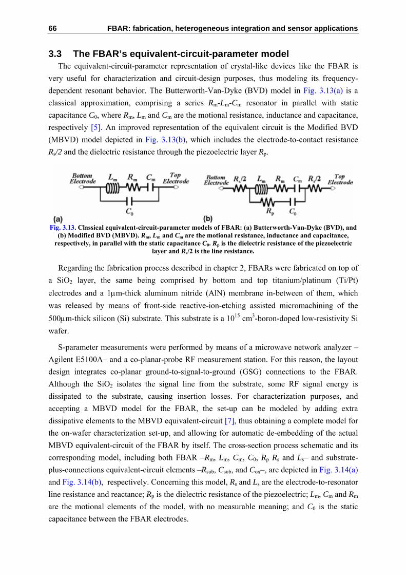
66 FBAR: fabrication, heterogeneous integration and sensor applications
3.3 The FBAR’s equivalent-circuit-parameter model The equivalent-circuit-parameter representation of crystal-like devices like the FBAR is
very useful for characterization and circuit-design purposes, thus modeling its frequency-dependent resonant behavior. The Butterworth-Van-Dyke (BVD) model in Fig. 3.13(a) is a classical approximation, comprising a series Rm-Lm-Cm resonator in parallel with static capacitance C0, where Rm, Lm and Cm are the motional resistance, inductance and capacitance, respectively [5]. An improved representation of the equivalent circuit is the Modified BVD (MBVD) model depicted in Fig. 3.13(b), which includes the electrode-to-contact resistance Rs/2 and the dielectric resistance through the piezoelectric layer Rp.
Fig. 3.13. Classical equivalent-circuit-parameter models of FBAR: (a) Butterworth-Van-Dyke (BVD), and
(b) Modified BVD (MBVD). Rm, Lm and Cm are the motional resistance, inductance and capacitance, respectively, in parallel with the static capacitance C0. Rp is the dielectric resistance of the piezoelectric
layer and Rs/2 is the line resistance.
Regarding the fabrication process described in chapter 2, FBARs were fabricated on top of a SiO2 layer, the same being comprised by bottom and top titanium/platinum (Ti/Pt) electrodes and a 1μm-thick aluminum nitride (AlN) membrane in-between of them, which was released by means of front-side reactive-ion-etching assisted micromachining of the 500μm-thick silicon (Si) substrate. This substrate is a 1015 cm3-boron-doped low-resistivity Si wafer.
S-parameter measurements were performed by means of a microwave network analyzer –Agilent E5100A– and a co-planar-probe RF measurement station. For this reason, the layout design integrates co-planar ground-to-signal-to-ground (GSG) connections to the FBAR. Although the SiO2 isolates the signal line from the substrate, some RF signal energy is dissipated to the substrate, causing insertion losses. For characterization purposes, and accepting a MBVD model for the FBAR, the set-up can be modeled by adding extra dissipative elements to the MBVD equivalent-circuit [7], thus obtaining a complete model for the on-wafer characterization set-up, and allowing for automatic de-embedding of the actual MBVD equivalent-circuit of the FBAR by itself. The cross-section process schematic and its corresponding model, including both FBAR –Rm, Lm, Cm, C0, Rp Rs and Ls– and substrate-plus-connections equivalent-circuit elements –Rsub, Csub, and Cox–, are depicted in Fig. 3.14(a) and Fig. 3.14(b), respectively. Concerning this model, Rs and Ls are the electrode-to-resonator line resistance and reactance; Rp is the dielectric resistance of the piezoelectric; Lm, Cm and Rm are the motional elements of the model, with no measurable meaning; and C0 is the static capacitance between the FBAR electrodes.

Chapter 3. FBAR device: characterization and modeling 67
Fig. 3.14. Equivalent-circuit-parameter model of the FBAR including substrate loss and reactance
elements: (a) Cross-section processes schematic with model; (b) Equivalent-circuit model; (c) Characterization set-up detailing GSG probes; and (d) Equivalence between actual devices and model
parameters.
Fig. 3.14(c) shows the GSG connections to a sample FBAR, and the optical micrograph of Fig. 3.14(d) relates the equivalent-circuit parameters with the FBAR’s layout.
3.4 Low frequency measurements Low frequency measurements are intended to verify appropriate functionality of the device
and, at the same time, to extract basic electrical and mechanical parameters of the materials composing the FBAR. We define “low-frequency” as the frequency range comprised between DC to a few MHz, namely the frequencies in which the first mechanical modes of the FBAR are found. First, the integrity of the device is verified by DC short-open measurements, which allow the evaluation of the pad and transmission line DC resistance (Rs/2). Next, the static capacitance C0 is measured in fully-operable devices, i.e. those resonators in which the short-circuit condition is not verified (between bottom and top electrodes). The static permittivity ε value is then extracted from the measured C0 value, given that the device-layout dimensions are known (electrode area A and thickness t of the AlN layer). On the other hand, low-frequency measurement of the fundamental electro-mechanical resonance frequency provides useful information for the extraction of purely-mechanical AlN parameters. A complete list of the instrumentation used in the low-frequency measurements is provided in Annex VI.

68 FBAR: fabrication, heterogeneous integration and sensor applications
3.4.1 Short-open DC measurements Short and open-circuit measurements allowed analyzing the integrity and proper
functionality of the resonator, and were performed using a Micro Tec DC probe station (Karl Süss) and a semiconductor parameter analyzer (Hewlett-Packard 4155B). A fully-functional device must accomplish both short and open-circuit conditions. For I/V testing and set up, a saturation current was defined for the short-circuit measurement. Also, we used I(V) plots to evaluate the line resistance: a high resistance prompts for the open-circuit verification, whilst low-resistance values are indicative of the short-circuit condition (line resistance in the units of ohm).
The short-circuit condition was verified by connecting two DC probes at different points of a given electrode, as shown in Fig. 3.15(a) and Fig. 3.15(b). Due to the fabrication process and to the device’s layout, it was of special interest to check out this condition on the top electrode: since high steps of this layer arise between the devices and transmission-line-to-pad areas, the risk of open-circuit had to be evaluated. Hence, the short-circuit condition is verified if the electrode shows current-continuity between the points where the two probes are located on. The experimental I/V plot for a device verifying the condition is shown in Fig. 3.15(c). According to these measurements and to a current-limitation value of 100mA, the line resistance Rs/2 was estimated to be 12 Ω. It is to be noted that the location in which the probe touches the electrode has not been systematically controlled. Hence, this experiment was conceived only to give a rough estimation of the magnitude of Rs/2. Its value depends on the transmission line’s dimensions and fabrication materials. In our process, the line is made of Pt with thickness of 150nm, widths between 30-100μm and lengths between 50-200μm, which explains the high value of Rs/2, compared to Mo or Al implementations (Rs/2 less than 1Ω). Since Pt is a high resistivity material, compared to Al or Mo, for example, relatively short transmission lines lead to Rs/2 values of units of ohms. Thus, with appropriate layout and process optimization Rs/2 may be significantly reduced.
Fig. 3.15. Set up and connections for verification of the short-circuit condition: (a) side-view schematic of the probe location; (b) top-view optical photograph of fabricated FBAR indicating the probe location; (c)
I/V plot for a typical device (line resistance Rs/2 of 12 Ω).

Chapter 3. FBAR device: characterization and modeling 69
Open-circuit measurements were carried out by connecting one probe to the bottom electrode and the other one to the top electrode. In Fig. 3.16(a) and Fig. 3.16(b) the measurement configuration and connections are observed. Verification of the open-circuit condition guarantees that both electrodes are isolated between them, i.e. no electrical contact occurs, thus keeping the static-capacitance behavior of the device at low frequencies. Mask misalignment during the fabrication process could derive into electrode contacting and short-circuiting of them. The open-circuit condition is thus verified if current-discontinuity is observed between the two probing points. In Fig. 3.16(c) I/V plot for a device verifying the open-circuit condition is shown (the current was also limited to 100mA). Calculating the mean value and standard deviation of the current, the DC through-resistance was estimated to be between 25-90 GΩ (or open-circuit condition).
Fig. 3.16. Verification of the open-circuit condition: (a) side-view schematic of FBAR with probe location; (b) top-view optical photograph of fabricated FBAR indicating the probe location; (c) I/V plot for a device
verifying the condition (min. through-resistance of 25 GΩ, i.e. open-circuit condition).
3.4.2 Static capacitance and permittivity Once a device has passed both the open and short-circuit conditions, static capacitance C0
measurements allow evaluating the dielectric properties of the acoustic AlN layer. For this purpose, two-probe measurements were performed using a capacitance meter (Hewlett-Packard 4280A) and a MicroTec probe station (Süss). After measuring of the C0 value of various device geometries, the permittivity value can be estimated. The absolute permittivity ε, also known as dielectric constant, is defined as the dielectric displacement per unit electric field. Using the same notation defined in section 1.1, the first subscript gives the direction of the dielectric displacement; the second gives the direction of the electric field, among them:
εT11 [F/m]: is the permittivity for the dielectric displacement and electric field in
direction 1 under conditions of constant stress, and
εS33 [F/m]: is the permittivity for the dielectric displacement and electric field in
direction 3 under conditions of constant strain

70 FBAR: fabrication, heterogeneous integration and sensor applications
The permittivity can be evaluated by means of the following characterization procedure [8], given that the static capacitance C0 formed by the electrodes and piezoelectric is measured:
a. Low frequency capacitance (C0) measurement b. Thickness (t) measurement (by means of Profile-meter or SEM) [9] c. Capacitor area (A): determined from the resonator’s layout d. Calculation of Permittivity (ε) by means of the following relation:
AtCr
ST00
/33/11 =⋅= εεε (3.4)
The evaluation of εT11 or εS
33 depends on the test structure to be chosen. In our case, we have evaluated εS
33 by using the parallel-plate structure of fabricated FBARs. Including the effects of under-etching in the layout of the device –bigger resonator area than that defined by the etching mask–, the characterization results of C0 and ε are shown in Table 3.1.
Table 3.1. Static capacitance and permittivity extraction
FBAR shape (rectangular,
dimensions include under-etching area)
C0 [pF] (theoretical)
C0 [pF] (experimental)
Permittivity ε (theoretical: 7.8×10⁻¹¹)
X-Large (250×190μm2) 3.74 4.50 9.74×10⁻¹¹
Large (200×140μm2) 2.21 2.60 9.29×10⁻¹¹
Medium (100×90μm2) 0.71 0.73 8.11×10⁻¹¹
Small (45×60μm2) 0.21 0.29 10.7×10⁻¹¹
X-Small (45×50μm2) 0.18 0.22 9.78×10⁻¹¹ Average value 8.96×10⁻¹¹ Standard deviation 7.38×10⁻¹²
Given an average εS33 value of 8.96×10⁻¹¹ F/m, the difference between extracted/measured
and theoretical values of C0 and ε is around 15%. These differences may find explanation on process and layout deviations. First, the thickness of the AlN is not uniform, its standard deviation being of around 10%, as previously analyzed in section 2.2.1. Also, the under-etching area estimation has considered a regular, rectangular shape, which may not be necessarily the case in the actual implementation. Anyway, the difference is one order of magnitude lower than the nominal values, which is a good starting point for further refinement of the parameters.
3.4.3 Mechanical properties The FBAR performance is mainly determined by the acoustic and mechanical properties of
the AlN layer. In this section, we show the characterization results on the elastic stiffness (or Young’s modulus), mass density and sound velocity of AlN. In order to extract these properties, the FBAR’s low-frequency mechanical resonance is estimated from the analytical

Chapter 3. FBAR device: characterization and modeling 71
model of the clamped-clamped beam resonator depicted in Fig. 3.17 and compared with finite-element-modeling (FEM) and experimental data from a network analyzer.
Assuming thin-metal electrodes, the resonance frequency of the clamped-clamped beam structure shown in Fig. 3.17 mainly depends on the thickness t and length l of the AlN beam, and is calculated by [5]:
ρπ 12273.4
2
2
0c
ltf ⋅= (3.5)
Measuring the fundamental resonance frequency f0, the quotient of the stiffness constant c and the mass density ρ can be determined. Assuming the value of one of these constants, the other one can be extracted. Two independent measurements performed on beams of different dimensions allow the complete the evaluation of this quotient. Specifically, we took two rectangular beams with identical thickness t of 1μm and different lengths l of 60 and 90 μm.
Fig. 3.17. Clamped-clamped beam resonator with dimensions
The layout of each device is observed in the insets of Fig. 3.18, where the fundamental and subsequent resonance frequencies of each one are plotted. As observed in Fig. 3.18(a), the 90μm-long device exhibits a fundamental frequency of 800 kHz. On the other hand, the 60μm-long device resonates at the higher frequency of 1.5 MHz, as shown in Fig. 3.18(b), which is explained by its more reduced dimensions. These results are in good agreement with the theoretical expectations of the clamped beam model described by equation (3.2) and with the results of FEM simulations in ANSYS ®.
In regard of the results of the three characterization methods, the resonance frequencies are found to be very similar within small error (%). In Table 3.2 the values of the first resonance modes obtained by experimental, ANSYS ® and analytical methods are compared. Using these results and solving c and ρ in equation (3.5), the AlN stiffness and density values are estimated to be between 180-220 GPa and 3.0-3.7 g/cm3, respectively. With these results at hand, the sound velocity can be derived through the well-known relationship [6]:

72 FBAR: fabrication, heterogeneous integration and sensor applications
Fig. 3.18. Mechanical resonances of the beam-shaped FBARs in the insets: (a) length of 90 μm, and (b)
length of 60 μm (thickness is 1μm for both devices).
ρυ c
= (3.6)
According to the extracted stiffness and density values, the sound velocity of the AlN implemented in this process is in the range of 7,000-8,500 m/s, which is below from the 9,500-10,500 m/s reference values. This reduction is explained by the characterized stiffness values, which are lower than the 300-360 GPa reference values. As it will be studied later, the acoustic velocity affects the high-frequency resonant behavior of the device, although other electro-mechanical parameters have to be also accounted for.

Chapter 3. FBAR device: characterization and modeling 73
Table 3.2. Low-frequency characterization of FBAR, comparing experimental; finite-element-modeling (ANSYS®) and analytical calculations for a clamped-clamped beam resonator
Device Experimental (S-parameter data)
Finite-element-modeling (ANSYS ®)
Analytical (equation 3.2)
Medium Rectangular (width: 50μm, length:
90μm, thickness: 1μm)
1st mode (fundamental): 800 kHz
2nd mode: 1.3 MHz
3rd mode: 2.2 MHz
1st mode (fundamental): 877 kHz
2nd mode: 1.46 MHz
3rd mode: 2.47 MHz
1st mode (fundamental): 885 kHz
Small Rectangular (width: 50μm, length:
60μm, thickness: 1μm)
1st mode (fundamental): 1.5 MHz
2nd mode: 2.75 MHz
1st mode (fundamental): 1.98 MHz
2nd mode: 2.65 MHz
1st mode (fundamental): 1.9 MHz
3.5 High frequency measurements High-frequency measurements are intended for evaluation of the frequency response of the
resonator above several hundreds of MHz and the GHz bands. In this high-frequency range band the resonant behavior of the FBAR is described by equation (1.2), for longitudinal-mode propagation of the acoustic wave through the bulk of the resonator.
In this work, high-frequency characterization of the FBAR was focused on S-parameter measurements and analysis. As previously studied, the resonant behavior at these frequencies is mainly determined by the mechanical and piezoelectric properties of the active layer (AlN), and by the process implementation (thickness of the AlN and metal-electrode layers). In this section, the S-parameters of various types of FBARs are described. From this description, the quality factor, electro-mechanical coupling coefficients and piezoelectric constants were extracted. The effects of the device’s layout in the electrical response and generation of lateral, spurious resonance modes is also discussed. The electrical response and fabrication process is analyzed for FBAR-based ladder filters as well, which were fabricated after the RIE-assisted process described in the previous chapter. A complete list of the high-frequency measurement instrumentation is provided in Annex VI.

74 FBAR: fabrication, heterogeneous integration and sensor applications
3.5.1 S-parameter description For each one of the devices of section 3.2, high-frequency S-parameter measurements were
performed. Where fabrication results have allowed, some devices were implemented using more than one micro-machining technology. Also, slight process variations were introduced in selected devices, mainly on the thicknesses of the electrodes and the AlN layer.
Type I: The irregular rhomboid device
The irregular rhomboid device was implemented according to the three processes described in chapter 2. The curves of Fig. 3.19(a) compare the frequency response of the S21 parameter of different devices released by front-side RIE, surface, and back-side bulk micromachining. The electrodes are made of Ti/Pt (30nm/150nm) and the AlN layer has a thickness of 1μm. With this configuration, the studied FBARs resonate at 2.3 GHz, although differences in the frequency response are observed between them. As evidenced, the RIE-based process provides a device with much better electrical response and quality factor. It can be noted the differences on the resonance frequency between the RIE-based (front-side) and the KOH-released (back-side) devices, which is explained in part for the location in the wafer of the tested devices. This makes the AlN layer to be of different thicknesses in such cases due to non-planarization of the process, as explained in chapter 2. Other explanation is the added thickness of the FBAR-stack in the back-side etching case (a Si3N4 membrane underneath the first electrode prevents the FBAR structure to be damaged by the KOH attack). This difference is a constant for all the KOH-etched devices presented in this work. Also, we compared the performance of FBARs with electrodes made of different adhesive metals. For this purpose we prepared two wafers, one with Pt deposited on Ti, and the second one with Pt deposited on Cr. Both wafers were processed by means of back-side wet etching in KOH solution.

Chapter 3. FBAR device: characterization and modeling 75
Fig. 3.19. S-parameter characterization of the Irregular rhomboid FBAR (type I): (a) three micro-
machining processes are compared, the RIE-based one achieving the best electrical response. The FBAR configuration and layer thicknesses are: AlN (1μm), Ti/Pt (30nm/150nm); (b) Influence of the electrode
composition in the frequency response (Cr/Pt against Ti/Pt, 30nm/150nm each)
The curves of Fig. 3.19(b) show that for the Cr/Pt (30nm/150nm) electrodes strong spurious resonances appear, whereas in the Ti/Pt (30nm/150nm) case only the main longitudinal-mode resonance is observed. The reason for this difference is unknown, although a modification in the Pt substrate (due to its adhesive metal) may have induced a variation in the AlN’s crystallographic configuration. Also, it could happen that different etching conditions affecting the final thickness of the Si3N4 membrane leaded to modification of the phase conditions through the stack and allow the generation of these resonances to appear. This could also explain the differences in the resonance frequency. This subject is to be further studied.
Further process variations were also tested on these devices. For example, the thicknesses of the AlN and of the electrodes layers were changed, in order to achieve higher resonance frequency values. In the plot of Fig. 3.20(a) the S21 parameter of an FBAR made with an AlN membrane of thickness 500nm (Ti/Pt thicknesses are the same as for the previous device). It can be observed an increase in the resonance frequency, the same being 3.1 GHz. Also, the electrode metallization was compared for the 500nm-thick AlN. The same metal configurations studied in the previous case (Ti/PT and Cr/Pt, 30/150nm) were implemented. The curves of Fig. 3.20(b) show again that strong spurious resonances appear for the Cr/Pt electrode case.

76 FBAR: fabrication, heterogeneous integration and sensor applications
Fig. 3.20. S-parameter characterization of the Irregular rhomboid FBAR (type I): with thinner AlN layer
(500nm-thick): (a) RIE vs KOH processes showing a resonance frequency of 3.1 GHz (thicknesses of Ti/Pt: 30nm/150nm); (b) Influence of the electrode composition in the frequency response (Cr/Pt against
Ti/Pt, 30nm/150nm each)
In another experiment the electrode-thickness influence was analyzed for the 500nm-thick-AlN devices. As observed in Fig. 3.21, the thicker-electrode device resonates around 3 GHz, whereas the thin-Cr/Pt-electrode (30nm/50nm) exhibits high-frequency harmonics, the main resonance appearing to be located around 4.5-5.0 GHz (no data available for the first case above 3.5 GHz).

Chapter 3. FBAR device: characterization and modeling 77
Fig. 3.21. S-parameter characterization of the Irregular rhomboid FBAR (type I) with metal electrodes of
different thicknesses (Ti/Pt, 30nm/150nm vs. 30nm/50nm)
Type II: The decagon device with holes (“The Orange”)
The decagon device with holes was implemented according to the three processes described in chapter 2. However, for the back-side KOH-etching process, the layout of this device appears to be too fragile for the device to be characterized. The curves of Fig. 3.22 compare the frequency response of the S21 parameter of different devices released by front-side RIE and surface micromachining. The electrodes are made of Ti/Pt (30nm/150nm) and the AlN layer has a thickness of 1μm. With this configuration, the studied FBARs resonate at 2.3 GHz, although differences in the frequency response are observed between them. As evidenced, the RIE-based process provides a much better device. The low performance of the surface-based device could be due to incomplete release of it.
Fig. 3.22. S-parameter characterization of the Decagon FBAR with holes – The Orange (type II): RIE vs.
surface-micro-machined devices showing a resonance frequency of 2.3 GHz (thicknesses of Ti/Pt: 30nm/150nm)

78 FBAR: fabrication, heterogeneous integration and sensor applications
Type III: The decagon device with no holes
The decagon device without holes was also implemented according to the same three processes described in chapter 2. Although it has the same shape of the Orange, it demonstrated less fragility, surely due to its more compact structure (no holes weakening the structure). The curves of Fig. 3.23 compare the frequency response of the S21 parameter of different devices released by front-side RIE and surface micromachining. The electrodes are made of Ti/Pt (30nm/150nm) and the AlN layer has a thickness of 1μm. With this configuration, the studied FBARs resonate at 2.3 GHz, although differences in the frequency response are observed between them. Again, the RIE-based process exhibits the best performance.
Fig. 3.23. S-parameter characterization of the Decagon FBAR with no holes (type III): RIE vs. surface-micro-machined devices showing a resonance frequency of 2.3 GHz (thicknesses of Ti/Pt: 30nm/150nm)
Type IV: The round-shaped device
The round-shaped FBAR was also implemented according to the same three processes described in chapter 2. Devices released by surface-micromachining were not available for characterization. The curves of Fig. 3.24 compare the frequency response of the S21 parameter of two different devices released by front-side RIE and back-side bulk micromachining. The electrodes are made of Ti/Pt (30nm/150nm) and the AlN layer has a thickness of 1μm and the resonance frequency is 2.3 GHz. In the general case, the RIE-based process exhibits the best performance.

Chapter 3. FBAR device: characterization and modeling 79
Fig. 3.24. S-parameter characterization of the Round-shaped FBAR (type IV): RIE vs. back-side bulk-micro-machined devices showing a resonance frequency of 2.3 GHz (thicknesses of Ti/Pt: 30nm/150nm)
Type V: The rectangular device (medium)
The rectangular device was among the FBARs exhibiting one of the best electrical performances. Two device implementations were characterized; the first one based on front-side RIE and the second one on surface micromachining. As observed in Fig. 3.25, the S21 magnitude of the RIE implementation exhibits big resonance peaks, although strong lateral resonances are observed. This can happen due to the presence of an under-etched SiO2 membrane supporting the device (it does not occur in the surface-based device). Although it has a low quality-factor, the surface micro-machined device can be released after few minutes immersed on the buffered HF solution (<5 minutes). Due to its good electrical response, this device was implemented in the sensor applications that are explained in chapter 5.
Fig. 3.25. S-parameter characterization of the Rectangular FBAR – Medium (type V): RIE vs. surface-micro-machined devices showing a resonance frequency of 2.3 GHz (thicknesses of Ti/Pt: 30nm/150nm)
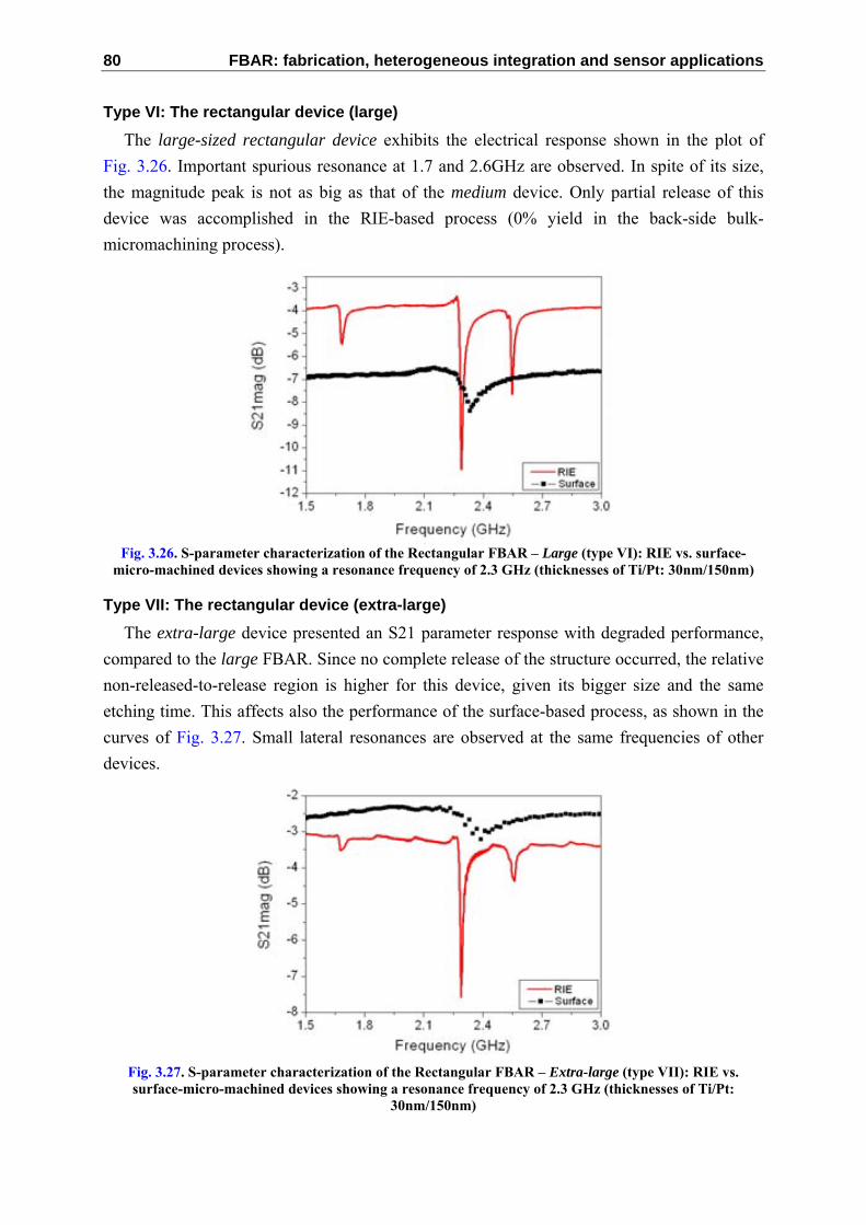
80 FBAR: fabrication, heterogeneous integration and sensor applications
Type VI: The rectangular device (large)
The large-sized rectangular device exhibits the electrical response shown in the plot of Fig. 3.26. Important spurious resonance at 1.7 and 2.6GHz are observed. In spite of its size, the magnitude peak is not as big as that of the medium device. Only partial release of this device was accomplished in the RIE-based process (0% yield in the back-side bulk-micromachining process).
Fig. 3.26. S-parameter characterization of the Rectangular FBAR – Large (type VI): RIE vs. surface-
micro-machined devices showing a resonance frequency of 2.3 GHz (thicknesses of Ti/Pt: 30nm/150nm)
Type VII: The rectangular device (extra-large)
The extra-large device presented an S21 parameter response with degraded performance, compared to the large FBAR. Since no complete release of the structure occurred, the relative non-released-to-release region is higher for this device, given its bigger size and the same etching time. This affects also the performance of the surface-based process, as shown in the curves of Fig. 3.27. Small lateral resonances are observed at the same frequencies of other devices.
Fig. 3.27. S-parameter characterization of the Rectangular FBAR – Extra-large (type VII): RIE vs. surface-micro-machined devices showing a resonance frequency of 2.3 GHz (thicknesses of Ti/Pt:
30nm/150nm)

Chapter 3. FBAR device: characterization and modeling 81
Type VIII: The rectangular device (small)
The small device is an interesting case for comparative analysis of the processes. Probably due to its reduced size, similar S-parameter response was observed for this resonator, when fabricated within the RIE and the surface micromachining processes.
As observed in Fig. 3.28, the size of the main resonances is very similar in both cases. The high fabrication yield within the surface-based process allowed characterization of enough devices, and due to the low etching-times (less than three minutes) less impact in the structure was observed. In contrast, the RIE-based device was released after 240 minutes, due to in-parallel processing with bigger devices. An additional advantage of the small’s surface-based realization is the absence of significant spurious resonances. Geometry optimization would contribute to reduce even more the smaller undesired resonances.
Fig. 3.28. S-parameter characterization of the Rectangular FBAR – Small (type VIII): RIE vs. surface-micro-machined devices showing a resonance frequency of 2.3 GHz (thicknesses of Ti/Pt: 30nm/150nm)
Type IX: The rectangular device (extra-small)
The extra-small device was fabricated and characterized upon the surface-micromachining process. Presumably, the minuscule size of the opening window imposed great resistance and difficulty to plasma-assisted micro-machining, thus minimizing the etching rate. The S21 parameter of an exemplary device can be seen in the plot of Fig. 3.29.

82 FBAR: fabrication, heterogeneous integration and sensor applications
Fig. 3.29.S-parameter characterization of the Rectangular FBAR – Extra-small (type IX): surface-micro-
machined device showing a resonance frequency of 2.3 GHz (thicknesses of Ti/Pt: 30nm/150nm)
Other devices
Other devices were also characterized. For example, the S21 parameter of the extra-extra-small device, which is a 5×10 μm2 rectangular device, is observed in Fig. 3.30(a). The same parameter is shown in Fig. 3.30(b), for RIE and back-side micromachining realizations of a cantilever-shaped FBAR (100×120 μm2, rectangular). These devices would have interesting applications in sensing systems, the first one due to its reduced size, the second one because of its presumably capability of force detection. Actually, an elaborated layout of the cantilever FBAR has been implemented for AFM force detection (this device is discussed in chapter 5).

Chapter 3. FBAR device: characterization and modeling 83
Fig. 3.30. S-parameter characterization of other devices: (a) Rectangular FBAR – Extra-extra-small,
surface-micro-machined device resonating at 2.3 GHz (thicknesses of Ti/Pt: 30nm/150nm); (b) Cantilever FBAR, RIE vs. back-side bulk micromachining device resonating at of 2.3 GHz (thicknesses of Ti/Pt:
30nm/150nm)
PCB versus probe station measurements
In section 3.1 the PCB-based and the coplanar probe station characterization setups were described. The implementation of two different characterization systems has an impact on the measurement’s performance: The PCB-based set up is practical for complex systems involving more than one FBAR device, such as non-conventional devices or hybrid FBAR-CMOS circuits. However, this flexibility is achieved at the cost of added losses and reactance due to the wire-bonding, and is few practical for single-resonator characterization. Also, additional –and non-negligible– design and prototyping effort has to be accounted.
The comparison of both systems was carried out by firstly measuring FBARs directly on-the-wafer, using the coplanar probe station. After data measurement and acquisition, the wafers were diced and testing chips glued and bonded to the PCB. The plots of Fig. 3.31 compare data from S-parameter measurements performed on a rectangular (medium) FBAR, according to the above-mentioned procedure. Three main resonances are observed for this device at 1.8, 2.4 and 2.6GHz. Although the electrical response is similar for both setups, the effects of added losses and reactance affecting the S-parameter values can be observed. Wire-bonding and PCB design optimization would aid diminishing the differences between both measurements.
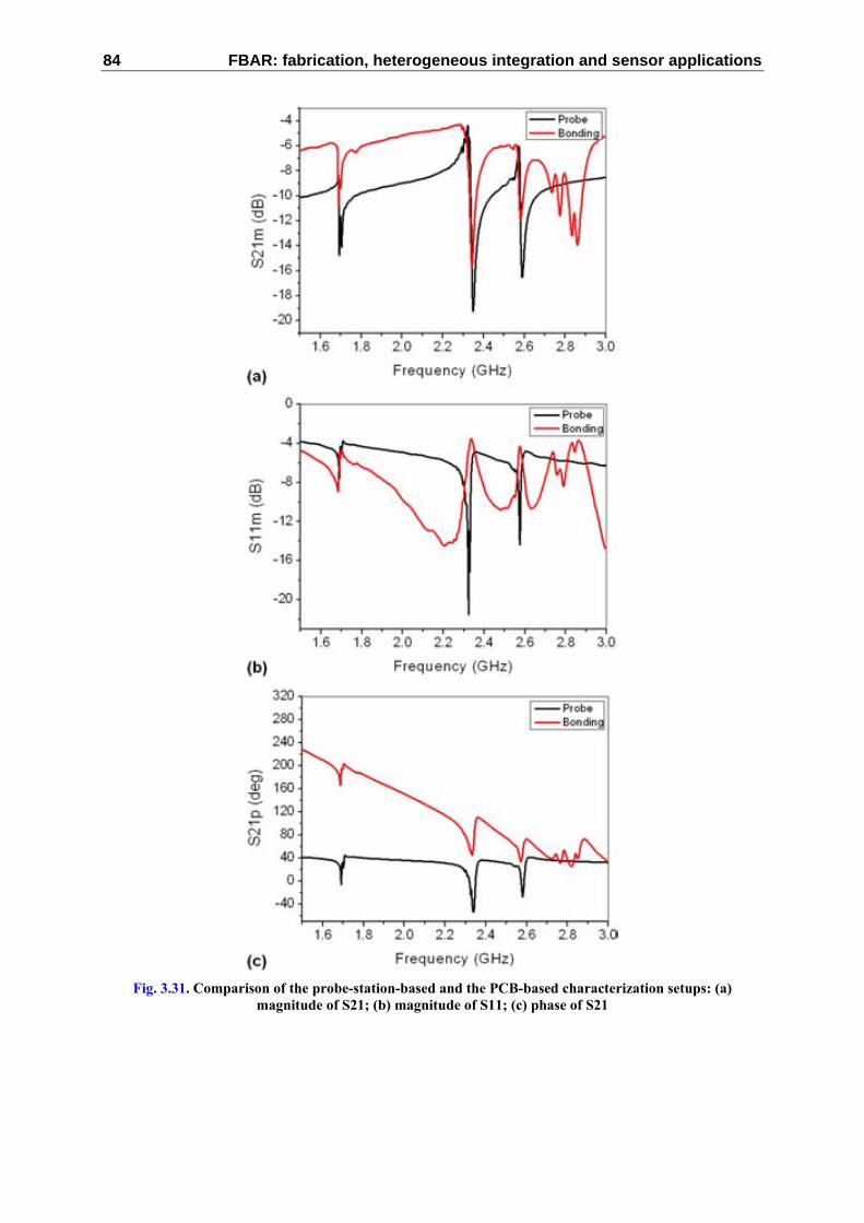
84 FBAR: fabrication, heterogeneous integration and sensor applications
Fig. 3.31. Comparison of the probe-station-based and the PCB-based characterization setups: (a)
magnitude of S21; (b) magnitude of S11; (c) phase of S21

Chapter 3. FBAR device: characterization and modeling 85
3.5.2 The quality factor The quality factor (Q) is a key parameter to evaluate the performance both the FBAR
devices and FBAR-based applications. Hence, its evaluation is of great concern in order to perform accurate estimations of the device’s capabilities. There are different methods for calculating the Q factor of a resonant device. Based on electrical characterization, transmission and reflection S-parameters are useful tools to extract the Q factor. Its characterization in FBARs is important because it determines the selectivity of filters and phase noise of oscillators in RF applications, and the sensing capability of sensors [10-11].
In a first method, which we will call the “S21-S11 magnitude method”, the Q-value of an FBAR can be obtained from two-port S-parameters measurement, using the magnitudes of both the transmission (S21) and reflection (S11) parameters. According to this method and assuming source impedance Zs of 50Ω, the Q factor is calculated by the following equation [2]:
( ) ( )Min
Min
Min
Min
p
S
p
S
S SS
SS
Q11
11
21
212
11
1
−−
⎟⎟⎠
⎞⎜⎜⎝
⎛−
⎟⎟⎠
⎞⎜⎜⎝
⎛
=
ωω
ωω
(3.7)
In equation (3.7) ωs and ωp are serial and parallel resonance frequencies, and S21Min and S11Min are the minimum values of S21 and S11 parameters, respectively. The advantage of this method for determining Q is that the derivation takes full account of acoustic and electrical loss mechanisms [12].
According to the classical BVD model, the Q factor at series resonance frequency can also be defined as:
mmSS CR
Qω
1= (3.8)
From equations (3.3), (3.7) and (3.8), values for Rm and Cm can be extracted in a first approximation by:
( ) SMin
Minm Z
SS
R 21 11
11
−= (3.9.a)
SmSm QR
Cω
1= (3.9.b)
Using this method, the Q factor at the longitudinal resonance frequency of 2.3 GHz was
calculated and preliminary R-L-C values were extracted. Table 3.3 shows some extracted values for RIE-based FBAR devices, an average Q value over 800 being obtained.

86 FBAR: fabrication, heterogeneous integration and sensor applications
Table 3.3. Q factor characterization using the “S21-S11 magnitude method”, and preliminary RLC
extraction for RIE-based FBAR devices
Device Q factor Rm [Ω] Lm [nH] Cm [fF] C0 [pF]
Type I 1,238 0.71 61.6 80.0 3.81
Type II 674 13.68 649 7.62 1.46
Type III 1,517 1.98 211 23.4 3.37
Type IV 289 17.69 358 13.7 0.38
Type V 519 9.22 335 14.6 0.70
Type VI 2,011 0.58 81.3 60.1 5.75
Type VII 541 1.96 74.2 66.2 4.21
Type VIII 338 120 283 1.72 0.14
Variations of the Q-factor value are explained by layout differences in size and geometry of the studied devices. On the other hand, the extracted Rm-Lm-Cm values give a rough idea of the FBAR’s performance.
Another definition of Q considers the open-loop phase response of the resonator φ(ω), examined at resonance. The Q is then defined as [11]:
ωφω
∂∂
=2
SQ (3.10)
If the phase slope is large, a significant change in the phase shift and Q factor arises. This
definition has an interesting interpretation for oscillator-design applications in which FBAR is the resonant device of the circuit: the open-loop value of Q is a measure of how much the closed-loop FBAR-and-circuit system will oppose to variations in the frequency of oscillation [11]. In practice, the Q factor at resonance is evaluated from the S21 parameter using this “phase-method”, by observing the derivative of the S21 phase (Fig. 3.32). The most negative derivative value coincides with the most negative phase slope, corresponding to the series resonance frequency fs. On the other hand, the most positive derivative value corresponds to the most positive phase slope, i.e. the parallel resonance frequency fp. Characterization results of the Q factor calculated by means of this method are similar to those found by the S21-S11-magnitude method. Average values over 1,000 are more optimistic than those obtained by the first method, although very useful for circuit-design purposes, as explained above.

Chapter 3. FBAR device: characterization and modeling 87
Fig. 3.32. Phase response of a typical FBAR for Q-factor calculation: (a) phase of the S21 parameter
indicating the minimum and maximum slope values (the same correspond to series and parallel resonance frequencies, respectively); (b) derivative of the S21 phase (the most negative and positive peaks
correspond to fs and fp)
A third method widely employed for Q-factor calculation recalls on the -3dB definition of bandwidth: Q is then defined as the resonance frequency divided by the two-sided -3dB bandwidth. This method is very popular for high-insertion-loss MEMS devices and band-pass filters with several-dB peak response. However, in low-loss devices such as FBAR, the resonance peak at the series-resonant frequency is poorly defined, especially –and paradoxically– in high-Q factor resonators (insertion-losses near to 0dB are the rule on FBAR performance). For this reason, this method is rarely used to characterize FBARs. Consequently, we have restricted the Q-factor measurements to the first two methods.
3.5.3 The piezoelectric coupling coefficient The piezoelectric coupling coefficient is, together with the Q factor, the most important
parameter characterizing the electrical performance of an FBAR. Strictly speaking, what is being characterized is the electro-mechanical conversion capability of the acoustic layer of the

88 FBAR: fabrication, heterogeneous integration and sensor applications
resonator (AlN in this process). Furthermore, a mutual relationship exists between them, through the figure of merit (FoM) of the resonator:
2TkQFoM ⋅= (3.11)
This means that, for a given technology, the value of the process is given by the combined
Q by kT2 product, rather than for only one of them. Depending on the application, it will be
interesting to optimize one of the Q or the kT2 values (the other one will diminish in the same
proportion).
Since piezoelectric ceramics are anisotropic, their physical constants (elasticity, permittivity, etc) are tensor quantities. For this reason the constants are generally expressed with two subscript indices referring to the directions of the detection-actuation physical variables, respectively. These variables are stress or strain (mechanical), or electrical displacement-electric field (electrical). The axes definition uses the same notation employed in section 1.1. The direction of positive polarization is usually chosen to coincide with the Z-axis of a rectangular system of crystallographic axes X, Y, and Z, as depicted in Fig. 3.33 (the directions of X, Y, and Z are represented by 1, 2 and 3, respectively, whereas the shear about these axes is done by 4, 5 and 6, respectively). In a longitudinal-mode FBAR, the electric field is applied in the direction of the Z-axis (“3”), thus coinciding with the preferred crystal orientation (c-axis). For this kind of FBARs and due to the electric field, the crystal will also experience strain/stress in the Z-axis (“3”).
Fig. 3.33. Axes convention and directions of deformation
Also, a superscript index is used to indicate a variable that is kept at constant value. Hence, the coupling coefficient kT
2 of an FBAR can be measured in the longitudinal (“33”) or transverse (“31”) directions. Depending on the available test structures, one or both of these coefficients can be measured.
Longitudinal coupling coefficient k233
First, the longitudinal coupling coefficient k233 is evaluated. This is done by measuring of
the bulk resonance frequency (mode “33”), which is found in the 2GHz-band for a typical FBAR process like ours. Taking into account that the piezoelectric layer is supported and excited by bottom and top metal electrodes, the coupling coefficient k2
33 has direct
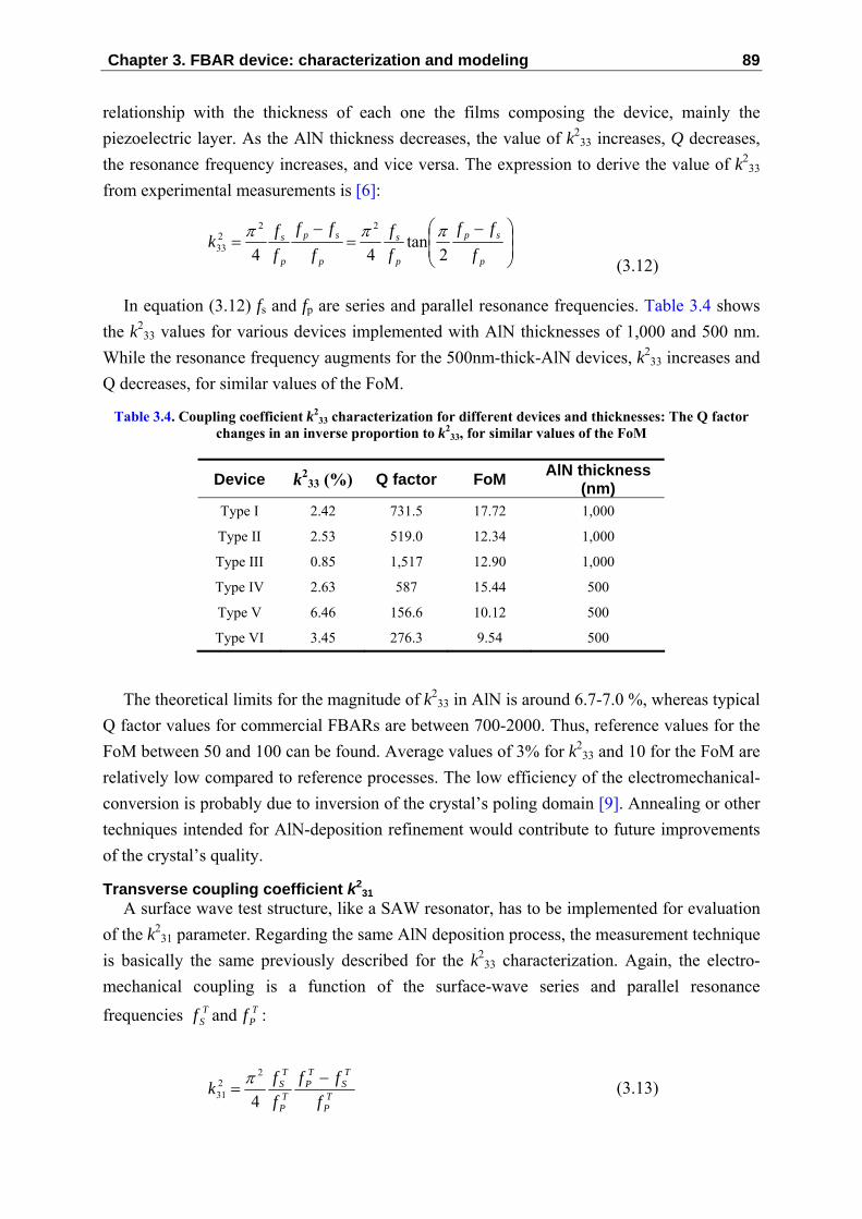
Chapter 3. FBAR device: characterization and modeling 89
relationship with the thickness of each one the films composing the device, mainly the piezoelectric layer. As the AlN thickness decreases, the value of k2
33 increases, Q decreases, the resonance frequency increases, and vice versa. The expression to derive the value of k2
33 from experimental measurements is [6]:
⎟⎟⎠
⎞⎜⎜⎝
⎛ −=
−=
p
sp
p
s
p
sp
p
s
fff
ff
fff
ffk
2tan
44
22233
πππ
(3.12)
In equation (3.12) fs and fp are series and parallel resonance frequencies. Table 3.4 shows the k2
33 values for various devices implemented with AlN thicknesses of 1,000 and 500 nm. While the resonance frequency augments for the 500nm-thick-AlN devices, k2
33 increases and Q decreases, for similar values of the FoM.
Table 3.4. Coupling coefficient k233 characterization for different devices and thicknesses: The Q factor
changes in an inverse proportion to k233, for similar values of the FoM
Device k233 (%) Q factor FoM AlN thickness
(nm) Type I 2.42 731.5 17.72 1,000
Type II 2.53 519.0 12.34 1,000
Type III 0.85 1,517 12.90 1,000
Type IV 2.63 587 15.44 500
Type V 6.46 156.6 10.12 500
Type VI 3.45 276.3 9.54 500
The theoretical limits for the magnitude of k233 in AlN is around 6.7-7.0 %, whereas typical
Q factor values for commercial FBARs are between 700-2000. Thus, reference values for the FoM between 50 and 100 can be found. Average values of 3% for k2
33 and 10 for the FoM are relatively low compared to reference processes. The low efficiency of the electromechanical-conversion is probably due to inversion of the crystal’s poling domain [9]. Annealing or other techniques intended for AlN-deposition refinement would contribute to future improvements of the crystal’s quality.
Transverse coupling coefficient k231
A surface wave test structure, like a SAW resonator, has to be implemented for evaluation of the k2
31 parameter. Regarding the same AlN deposition process, the measurement technique is basically the same previously described for the k2
33 characterization. Again, the electro-mechanical coupling is a function of the surface-wave series and parallel resonance
frequencies TSf and T
Pf :
TP
TS
TP
TP
TS
fff
ffk −
=4
2231
π (3.13)

90 FBAR: fabrication, heterogeneous integration and sensor applications
Thus, a SAW device was implemented, the same exhibiting series and parallel resonance frequencies of 211.75MHz and 212.15MHz, for an effective k2
31 value of 0.47%. This value is between one-fourth and one-fifth of the k2
33 value. Both k231 and k2
33 are utilized in the extraction of the piezoelectric constants of the AlN, which is explained in the following item.
3.5.4 Piezoelectric properties Piezoelectric properties of a fabricated material are process-dependent physical constants
explaining the electro-mechanical performance of the crystal. Although reference values are available for commercially available material compounds –like AlN–, specific crystal characterization has to be performed for a newly developed process. The piezoelectric constants can be expressed in voltage-to-strain (g), voltage-to-stress (d), charge-to-stress (e), and charge-to-strain (d) forms. Since linear relationships exist between the different forms, characterization of one form allows the knowledge of the other ones. In this section, the d-form of the piezoelectric constant is studied.
The piezoelectric constant d is defined as the electric polarization induced on a material per unit mechanical stress applied to it. Alternatively, it is the mechanical strain experienced by the material per unit electric field applied to it. The first subscript refers to the direction of polarization at zero-electric field (E = 0), or to the applied field strength. The second one refers to the direction of the applied stress, or to the direction of the induced strain, respectively. Two relevant components of the d-constant are:
d33 [m/V]: is the induced polarization per applied unit stress, both in the Z-axis (“3”). Alternatively it is the induced strain per unit electric field applied in the same direction.
d31 [m/V]: is the induced polarization in direction 3 per unit stress applied in direction 1. Alternatively it is the strain induced in direction 1 per unit electric field applied in direction 3.
Values of d33 and d31 can be extracted by different methods. A first method performs an experimental measurement of the mechanical displacement of the film when an electric potential is applied to the electrodes. The low absolute level of the displacements in thin-films necessitates the use of a precise interferometer technique. Typically, a resolution of about 10-2 Å and a complex measurement set up including a sensitive double-beam interferometer are required to determine the low-field piezoelectric coefficients [14]. For that reason, an indirect evaluation is preferred, by calculating the values of d33 and d31 from previously-extracted electromechanical constants.
In previous sections, FBAR and SAW resonators were of utility to evaluate permittivity, stiffness and coupling-coefficient constants. These constants can be used to obtaining the piezoelectric charge constants from piezoelectric constitutive equations:

Chapter 3. FBAR device: characterization and modeling 91
T
cdk
33
332332
33 ε⋅
= (3.14)
T
cdk
33
112312
31 ε⋅
= (3.15)
Solving the right-sided parts of (3.14) and (3.15) and using previously-extracted parameters, the d-constants are calculated. Thus, the values of d33 and d31 are 2.85 and 1.12 pm/V, whose magnitudes are roughly equal to a half the value of previously reported epitaxial AlN films [15]. The higher deposition temperatures of epitaxial processes partially explain the better quality of the films obtained with this process, compared to sputtered-AlN films. On the other hand, the d33/d31 value is 2.56, which is of the same order of the theoretical relationship for clamped wurtzite structures (d33/d31 = 2) [16].
3.5.5 Transmission-line modeling of the FBAR As piezoelectric-based devices, different analytical solutions to the wave equation in
FBARs have been proposed in the past, the most known being the Mason and KLM models
[17-19]. The Mason's model, for example, is able to show that for one-dimensional analysis
most of the difficulties in deriving the solutions could be overcome by borrowing from
network theory. Hence, it presents an exact equivalent circuit that separates the piezoelectric
material into an electrical port and two acoustic ports through the use of an ideal
electromechanical transformer. Each acoustic port represents the acoustic paths to the top and
bottom electrodes. For longitudinal-mode FBARs, the schematic and equivalent circuit
representations of the FBAR, according to the Mason-s model, are depicted in the schematic
drawings of Fig. 3.34.

92 FBAR: fabrication, heterogeneous integration and sensor applications
Fig. 3.34. Mason’s model of the FBAR: (a) cross-section view of the FBAR and layer’ impedances; (b)
equivalent circuit representation of the model
The input impedance Zin seen from the half-phase line of the AlN layer, between the two
parallel electrodes is:
( )( ) ( ) ⎟⎟
⎠
⎞⎜⎜⎝
⎛++++
++−×=
φφφφ
φφ
ω 2sin12cos2sincostan11 2
233
0 BTBT
BTin ZZjZZ
jZZkCj
Z (3.16)
Where φ is the half phase across the piezoelectric plate, k332 is the piezoelectric coupling
coefficient of the AlN film, C0 is the parallel-plate capacitance between the two electrodes,
and ZT and ZB are normalized acoustic impedances at the piezoelectric layer boundaries (with
respect to the acoustic impedance of the AlN layer). Equation (3.16) can be divided in three
components: one electrical, a second one purely mechanical and the third one depicted in Fig.
3.34 as the electro-mechanical transformer with gain N:
φφtan2
33kN = (3.17)
The phase across the piezoelectric layer is equal to:
t×= κφ (3.18)
Where κ and t are the wave vector and the thickness of the piezoelectric layer, and κ
depends on the frequency f and acoustic velocity v in the piezoelectric film, respectively:
vfπκ 2
= (3.19)
The boundary impedances ZT and ZB at the interface between the AlN and the electrodes
are determined by the relative impedance matching between both media. If more than one

Chapter 3. FBAR device: characterization and modeling 93
metal is used in the electrode's fabrication, or if another material is stacked, the acoustic path
to calculate the overall impedance should be modified. Both ZT and ZB can be found by:
⎟⎟⎠
⎞⎜⎜⎝
⎛++
×=BTLoadBT
BTBT
BTBTLoadBT
BT jZZjZZ
ZZ//
/0
//
0//0/ sincos
sincosφφφφ
(3.20)
Where Z0T/B is the characteristic acoustic impedance of either the top (T) or bottom (B)
electrode’s layer, ZLoad is the input load impedance seen by either the top or bottom
electrode’s layer at the next interface, and φT/Bs is the acoustic-wave phase across either the
top or bottom electrode’s layer. In FBARs the top and bottom surface of the electrodes have
an air interface (although in real implementations some area of the electrodes still contact the
substrate). Since air has low acoustic impedance, the air-to-electrode interfaces have boundary
impedances equal to zero. Final calculation of the electrical impedance Zin requires recursive
calculation of ZT and ZB, beginning from the air interfaces and ending at the AlN layer.
Based on this model and on previously-extracted electro-mechanical constants, the S-
parameter response of our FBARs was simulated. In Fig. 3.35 model against experimental
results are compared for a sample device. Assuming that calibration was carried out at the
closest point to the FBAR’s electrode (transmission line length L= 0), the S-parameters were
calculated from the Zin-to-S11 and Zin-to-S21 relationships described by equation (3.3).
An extension of this model is also implemented for explaining the mass-sensor
applications of FBAR, which will be described in chapter 5.
Fig. 3.35. Model against experimental results on the Mason’s model of FBAR: Electro-mechanical
constant values used in the model were taken from experimental extraction

94 FBAR: fabrication, heterogeneous integration and sensor applications
3.5.6 Layout effects on the high-frequency response Some electrode geometries have been demonstrated to suppress or diminish the presence of
spurious resonance modes than others [20]. These spurious modes are lateral, Lamb-like modes superposing to the main longitudinal-mode resonances, which appear due to the layout and the crystalline characteristics of the device. At the same time, the size of the electrodes has an effect in the insertion losses of FBARs [2, 21]. In order to study this subject, two groups of devices from the types described in section 3.2 were characterized and their frequency responses compared for the RIE-based process. The first group was composed of devices having non-parallel-shaped electrodes –types I to IV– and the second one of FBARs with parallel-wall electrodes –types V to IX–.
The S21 and S11 parameters of both groups were compared, observing two spurious resonances located near to 1.6 and 2.6 GHz in the parallel-side-electrode devices (Fig. 3.36(c)), whereas only a main resonance mode can be seen in the non-parallel devices of Fig. 3.36(d). The parallelism of the FBAR’s layout contributes to the appearance of important spurious resonances, due to the systematic transmission and reflection of lateral-mode waves.
Fig. 3.36. Electrode geometry influence in the electrical response of the FBAR: (a, b) parallel-rectangular and non-parallel-rhomboid side FBAR; (c, d) Electrical characterization for parallel and non-parallel side
devices (no important spurious modes are observed for the non-parallel cases).

Chapter 3. FBAR device: characterization and modeling 95
The addition of an ‘overlap’ electrode has also proven to be an effective means of reducing spurious-mode resonances [12, 21]. An overlap electrode is an annular-shaped structure built on the top electrode of the FBAR to modify the wave propagation conditions near the layout boundaries of the electrode. In this way a more uniform resonance shape is obtained, and the energy of lateral-mode resonances attenuated. The implementation of one or both strategies in order to optimize the FBAR’s layout will be addressed in future developments of this work.
3.5.7 FBAR-based ladder-filters Ladder filters and duplexers are nowadays the most popular and commercially successful
application of FBARs. Worldwide companies like Avago Technologies (formerly Agilent), or Infineon are selling millions of units each year, thus replacing RF components made with SAW and ceramic technologies [23-24]. These components offer lower-insertion losses, higher out-of-band rejection and more reduced size than those made with previous technologies.
Although FBAR filters are well developed and mature at both design and technology levels, we have implemented some FBAR-based filters for device characterization purposes. Since there are numerous references on FBAR filters [25, 26], this application has also become a useful benchmark tool in order to explore the limitations and possibilities of our FBAR technology.
The ladder filter is comprised by an nth-order interconnection of series and shunt-located FBARs as depicted in Fig. 3.37(a), the order of the filter being referred to the number of series-to-shunt stages, counting from the input to the output port of the filter [25].
A differential version of an FBAR-filter with no grounding connections is the lattice filter drawn in Fig. 3.37(b). In both topologies, the series and shunt FBARs have different resonance frequencies and should ideally be of different size, in order to optimize the in-band and out-of-band performance of the filter [27].
Fig. 3.37. FBAR-based filter topologies: (a) ladder filter (3rd order, 6 resonators); (b) lattice filter
(differential input-output ports)

96 FBAR: fabrication, heterogeneous integration and sensor applications
First, we have made the circuit-level design of ladder filters. The equivalent-circuit model of the FBAR was used to build a high-level model of the filter. Several model configurations of the filter were implemented, varying the FBARs size and the order of the filter. In order to implement the filters, new devices were designed and fabricated. The main concern about this task was the big resonator sizes and the long times required for front-side etching (besides of the structure’s weakening). For the ladder topology shown in Fig. 3.37(a), different realizations varying the electrode’s area and capacitance values of the shunt and series FBARs were implemented and their dimensions detailed in Table 3.5.
Table 3.5. Dimensioning of the filter’s size and capacitance values for series and shunt FBARs electrode area (adjusted for each topology)
Configuration AS (μm2) AP (μm2) C0S (pF) C0P (pF)
1 150×150 150×150 1.75 1.75
2 150×150 150×300 1.75 3.50
3 150×150 300×300 1.75 7.01
4 150×150 450×450 1.75 15.77
5 450×450 450×450 15.7 15.77
According to these configurations, circuit-level simulations were performed using both
Matlab ® and Cadence ® model implementations. The equivalent-circuit model of a 3rd-order filter (N=6 resonators) with 2.2 GHz central frequency and corresponding simulation results are shown in Fig. 3.38(a) and Fig. 3.38(b), respectively. Using previously extracted equivalent-circuit-parameter values, 2dB-insertion losses and out-of-band rejection higher than 36dB were predicted.

Chapter 3. FBAR device: characterization and modeling 97
Fig. 3.38. Circuit-level modeling of a 3rd-order ladder filter: (a) Cadence implementation of the equivalent-
circuit-model; (b) S21 frequency response (2dB-insertion loss, out-of-band rejection > 36 dB)
The collage in Fig. 3.39(a) shows optical micrographs of devices composing different filters. A detailed view of one of the irregular tetragon FBARs with holes is given in Fig. 3.39(b). As it can be seen, a diversity of size and geometry has characterized this design. Another important feature is the presence of through-holing, in order to reduce the etching time (looking at Table 3.5 and to previously described devices, the filter FBARs are much bigger, the smallest one having an area equivalent to the Extra-large rectangular resonator presented in section 3.2)
The electrical response of the 3rd-order, N=6 filter made of irregular tetragon FBARs with holes can be observed in the he plots of Fig. 3.40(a). This filter performs an insertion loss over 14dB and 26dB-zeroes at the out-of-band region, which are pretty poor for modern filter systems. These results evidence the need of further layout and process optimization, in order to reach competitive insertion loss and out-of-band rejection values.
Fig. 3.39. Fabricated devices for ladder-filter implementation: (a) a diversity of size and geometry, and
device-through-holing has characterized this design; (b) detail of one irregular tetragon FBAR with holes, used in the N=6-resonator design

98 FBAR: fabrication, heterogeneous integration and sensor applications
Fig. 3.40. S-parameter characterization of the 3rd-order ladder filter: (a) S21 magnitude of the N=6 filter;
(b) S21 parameter of the irregular tetragon FBAR composing the filter
Experimental insertion-loss and out-of-band rejection results are in good agreement with theoretical expectations and characterization of the stand-alone irregular tetragon FBAR with holes. Various resonators with this layout were analyzed, obtaining Q-factors between 63-83 and a k2
eff of 3.0-3.4%. The magnitude of the S21 parameter of a sample irregular tetragon device is shown in the plot of Fig. 3.40(b). With these values and according to the insertion-loss expression for a pass-band filter [28]:
⎟⎟⎟⎟⎟
⎠
⎞
⎜⎜⎜⎜⎜
⎝
⎛
+=
Qk
dBIL
eff2
234
4log20)(π
(3.21)
Insertion losses (IL) between 12-16 dB were predicted. These values are comparable with the IL observed in Fig. 3.40(a). The low Q-factor value is attributed to the through-holed design, which substantially reduced the electrode’s area, and the same is definitively less than the Q-factor values reported in section 3.5.

Chapter 3. FBAR device: characterization and modeling 99
Comparing these Q-factor values to those reported in section 3.5, a process optimization is to be initiated for the specific case of ladder filters. Since high Q-factors have been achieved to single-resonator applications (mass sensor, for example), layout and etching-time related issues are assumed to be the main factor degrading the filter’s performance. These and other design issues –like the in-band bandwidth of the filter– are to be studied in future stages of this work.
3.6 Equivalent-circuit-parameter extraction Previously on section 3.2.4 the BVD equivalent-circuit-parameter model of FBARs was
introduced. Electrical modeling and extraction of equivalent-circuit parameters in FBAR is well documented, the lumped-element Modified Butterworth-Van Dyke (MBVD) being the most accepted model for parameter extraction purposes. In [29], an off-resonance measurement procedure is proposed for the extraction of the six-parameter MBVD model in FBAR. This is carried out by evaluating and averaging the resistive and reactive components of the S-parameters evaluated at six different points in a frequency span where the resonance is expected to be found. This method, however, has not been explicitly presented to run any optimization process to extract the parameters, although it is mentioned that fitting in the least mean squares sense is performed. Also, it does not take into consideration possible additional dissipative elements in the model due to the substrate, because they perform on-the-wafer calibration. These dissipative elements are of great interest since they could explain insertion losses and signal drifting from the RF signal paths connecting the FBAR to the substrate wafer. This is particularly important to de-embed the FBAR model for CMOS-integrated applications. On the other hand, a genetic algorithm is proposed in [30] to extract the material parameters in FBAR, although without relating this extraction to an equivalent-circuit parameter model.
Concerning the optimization of parameter extraction in other RF devices, extensive work has been carried-out to extract, from measured S-parameters, the equivalent-circuit parameters of microwave resonators [31], FET transistors [32-33], and filters [34]. In most of these cases, a least-squares strategy is adopted to optimize the extraction of the circuit parameters. Thus, in considering previous work, a multi-step algorithm implementing a least-squares optimization strategy for the extraction of equivalent-circuit elements is presented. At the same time, extraction of the substrate model is performed. In this way, on-wafer calibration is avoided –as it is done in [29]–, allowing for model-based de-embedding of the MBVD parameters. This procedure saves wafer area and simplifies the set-up for characterization.
3.6.1 Parameter-extraction algorithm The extraction algorithm is an iterative multi-step implementation of a least-squares
estimation of the optimal values of the FBAR’s equivalent-circuit parameters. Each one of the

100 FBAR: fabrication, heterogeneous integration and sensor applications
steps in the algorithm extracts a sub-set of one or more of the equivalent-circuit parameters depicted in Fig. 3.14(b). On the other hand, sensitivity to S-parameters was analyzed, in order to determine the most adequate function to be used in the extraction of each circuit element. Thorough exploration of the model allowed us to find out that some elements are more sensitive to the reflection parameter S11, whereas others do to the transmission parameter S21. Also, the execution sequence of the steps was studied, with the aim of achieving good numerical stability and convergence rate. We present in Table 3.6 a summary of this study, where the seven different error-functions involved in each one of the seven steps of the algorithm are defined.
Table 3.6 Error functions of the multi-step parameter-extraction algorithm
Step Circuit-elements optimized
S-parameter fitted Error function
1 Rm S11 S11mag(Rm)
2 Lm, Cm, C0 S21 S21phase(Lm, Cm, C0)
3 Rs S11 S11mag(Rs)
4 Rp S21 S21mag(Rp)
5 Rsub S21 S21mag(Rsub)
6 Csub S21 S21phase(Csub)
7 Cox S21 S21phase(Cox)
The number of iterations is set in two ways: first, by means of an internal tolerance value
of the error-function value, and, in parallel, by user’s setting as a running parameter at the time of execution of the algorithm. At its time, the execution of each sub-step may be controlled by means of various optimization criteria. Since each sub-step is also an iterative routine by itself, one of the optimization criterions may be the number of local execution cycles (for the sub-step, with independence of the global number of iterations). Other optimization criteria may be the tolerance of the optimized variable, or the tolerance of the error-function value, among others. Around ten global iterations are typically enough for achieving good convergence of the equivalent-circuit parameters in a standard Pentium-processor-based PC-platform.
For a given iteration cycle Rm is optimized in the first step of the algorithm. The remaining elements in the equivalent-circuit are then set to fixed values, just the ones obtained by the algorithm in the previous iteration cycle. In the second step, the L-C-C0 sub-set is optimized, Rm and the remaining elements being fixed to constant values. In this step, the second error-function –according to Table 3.6– is implemented for optimization of L-C-C0. Once finished this step, the algorithm proceeds in the same way to execute the following steps until the seventh step is finished. In that moment a new global cycle starts, and the foregoing process is

Chapter 3. FBAR device: characterization and modeling 101
repeated until the last iteration is completed. Additional routines are carried out by the algorithm, in order to complete the full-automated parameter-extraction procedure, including: loading of S-parameter ASCII data and first estimation of the BVD parameters [2], among others.
3.6.2 Experimental results on the extraction of parameters The optical image of Fig. 3.41(a) shows a top view of a rectangular FBAR (medium size,
type V) with annotated model elements, according to the process already described in section 3.3.1. The dark area around the resonator is Si under-etching underneath the SiO2 layer (an equivalent area can be found underneath the FBAR). Experimental and extraction results are plotted in Fig. 3.41(b), where the transmission spectrum (S21) magnitude is appreciated in a span of 1.5 GHz. These results are compared with both MBVD and BVD models curves, as well. For the layout configuration of the device in Fig. 3.41(a), the extracted values are in the same order of magnitude than those expected from the theoretical analysis: For a Ti/Pt transmission line of thickness 30nm/150nm, width 50μm and length 250 μm, theoretical Rs/2 and Ls/2 are in the range of 8-12 ohm and 90-140 fH, respectively. Extracted values for Rs/2 and Ls/2 are 12.25 ohm and 34 fH, respectively.
Fig. 3.41. Experimental results on the extraction of FBAR’s parameters: (a) Exemplary FBAR with
annotated model elements; (b) Fitting and experimental curves (BVD and MBVD curves are also plotted)

102 FBAR: fabrication, heterogeneous integration and sensor applications
Concerning the substrate of FBAR, an 800nm-thick thermal-SiO2 layer leads to theoretical value of Cox of around 430 fF, whereas the extracted value is 647 fF. On the other hand, theoretical calculations for our low-resistivity 500μm-width Si wafers result in values in the range of 2,000-10,000 Ω and 2fF for resistance Rsub and capacitance Csub, respectively. These values are of the same order to the extracted values obtained by the algorithm, the same being 150 Ω and 1fF, respectively. Differences in the extracted and theoretical values of Rsub may be explained by a lower resistivity value of the wafer, respect to the expected doping configuration. Further characterization of this process should allow refinement of this parameter. Whatever the case, the extracted values are consistent with the properties of a low-resistivity substrate.
Finally the BVD-model’s extracted values are also closely related to experimental observation. In particular, for the testing device, the measured coupling coefficient keff
2 of 2.32% is very close to 2.22%. The latter is calculated from the extracted values of Lm, Cm, C0; 435.5nH, 11.1fF and 605.2fF, respectively. Also Rm and Rp of 10 and 8.5 Ω are values in the range of those of previously reported resonators.
In summary, fabricated FBARs have been modeled on-the-wafer. Based on this model, an algorithm implementing automatic parameter extraction in FBAR has been developed [35-37]. In this way, on-wafer calibration may be avoided thus achieving instantaneous de-embedding of resonator parameters. Experimental results show good agreement between experimental and extracted values. This algorithm allows for rapid and efficient characterization of FBAR and the substrate wafer. Taking into consideration that the algorithm extracts purely electrical-parameters, future developments of this work might include the integration of the electrical-domain with other-domain parameters, for the extraction of piezoelectric coefficients or mechanical constants, for example.
3.7 Process deviations and stability
3.7.1 AlN thickness tolerance As previously stated in chapter 1, the thickness of the AlN layer mainly determines the
resonance frequency of FBARs. Also, the overall resonator performance depends on how accurately the resonance frequency’s value is designed. Additionally, time and temperature stability are critical factors on the frequency stability. Thus, determining the tolerances of each issue is of great importance for the development of a viable manufacturing process.
In certain applications, like FBAR-based ladder filters, the resonance frequencies f1 and f2 of both the series and the shunt resonators, respectively, have to be fixed within very small tolerances in order to preserve the bandwidth-to-central frequency, in-band insertion loss and out-of-band-rejection specifications. Since the size and frequency relationship of both devices have a big impact on the filter’s response, small tolerances are allowed to obtain final

Chapter 3. FBAR device: characterization and modeling 103
products with feasible and market-attractive performance. As previously discussed, the AlN thickness is the key process parameter controlling the resonance frequency of the filter-composing FBARs. For example, the analysis in [38] shows that a deposition process of ZnO with thickness tolerance of ±86Å is required to obtain a competitive ladder filter with application in the PCS band (1.9 GHz). As reported on section 2.2.1, thickness and profile measurements of the AlN layer were carried out. Now, S-parameter characterization for different devices confirms that the resonant-frequency deviations are of the same order of the thickness deviations previously found, i.e. between 10-15%, as observed in the plot of Fig. 3.42. Also commented in preceding sections, a planarization process is mandatory to reduce the variation of the AlN thickness, according to target values.
3.7.2 Time stability Time stability is also an important factor to be considered when studying the FBAR’s
frequency response. To analyze the fluctuations of the resonant frequency, we distinguish two cases: short-term and long-term stability. Short-time stability can be explained by noise sources in the set up. It can be studied in two ways: a) observing a wide-band frequency span of the resonant signal of the FBAR and acquiring various sets of data to calculate the frequency deviation; and b) observing a zero-Hz frequency span near to the resonance frequency to evaluate the phase deviation. An example of the second method is observed in the zero-span frequency plot of Fig. 3.43. This plot shows a phase-response acquisition of a rectangular FBAR (type V), taken at its series resonance frequency. To calculate the short-time frequency stability the mean phase deviation in this plot is divided by the phase slope evaluated at this frequency, which is calculated by differentiating the phase curve (see an example of phase differentiation in Fig. 3.32). In this example, the phase deviation is ±0.08 deg and the phase slope is 2.6×10⁻⁶ deg/Hz. Consequently, the frequency drifting has a value of 30 kHz.
Fig. 3.42. Resonance frequency of FBARs with different AlN thicknesses: due to process deviations and
non-planar AlN deposition, both the thickness and resonant frequency present a 10-15% tolerance (respect to the nominal value).

104 FBAR: fabrication, heterogeneous integration and sensor applications
Fig. 3.43. Short-term time stability characterization: zero-span frequency-domain acquisition of the S21
phase response
Long-term stability was preliminary observed by performing S-parameter characterizations of various devices in a one-month period. The curves of Fig. 3.44 illustrate the magnitude of the S11 parameter of an exemplary device. These measurements were taken at room temperature with a temporal separation of one month between each one, with no significant difference of the resonance frequency among them. Although these results only give a rough idea of the FBAR’s stability, a more systematic study on long-term stability is to be performed on future stages of this work. For example, the minimum frequency resolution has to be explored, in order to establish accurate reference-frequency values.
3.7.3 Temperature stability and thermal coefficient factor (TCF) Temperature stability has been the third aspect studied in this work. In reference oscillator
applications of FBAR, for example, a low temperature coefficient (TCF) of the resonator is particularly important to guarantee the best phase-noise performance [39].
Fig. 3.44. Time stability characterization: two independent measurements of the S11 parameter were
performed on the same device with a one-month difference between them

Chapter 3. FBAR device: characterization and modeling 105
The set-up required for performing thermal characterization of FBARs include a network analyzer, a heater stage and temperature controller, and an appropriate probe station to allow easy temperature control. First, a reference temperature is defined and the S-parameters are measured. Next, the temperature is changed and controlled to perform successive S-parameter measurements, each one corresponding to the actual temperature. Changes on the resonance frequency will be annotated and related to the corresponding measured temperature. At the end, a curve relating resonance frequency against temperature is obtained. The frequency change is usually expressed in fractional form referred to the frequency at reference temperature per million units of frequency [ppm] as:
( )
][10][10 6
0
6
0
0 ppmffppm
fff i ×
Δ=×
− (3.22)
In equation (3.22) fi is the measured resonance frequency at temperature i, and f0 is
resonance frequency at the reference temperature. The plot of Fig. 3.45 shows the TCF of a rectangular device (type V: medium size), the thermal characterization being performed in a range of 100 ºC. The measurements were carried out at the EPSON’s characterization laboratories located in Hirooka, Japan.
A TCF between -12 and -20 ppm/ºC was measured on various devices. These values are in accordance to ANSYS ® 3D finite-element-modeling results provided by EPSON, which are of -16 ppm/ºC for a resonator with the same layer configuration. Also, it is known that the typical temperature coefficient of FBARs fabricated with sputtered AlN films is found in the -20 to -40 ppm/ºC. However, this TCF value is rather high to accomplish the requirements of modern RF applications. For this reason, optimization of the TCF towards a temperature-compensated device is discussed in the next section, where the involved processes and the first results are presented.
Fig. 3.45. Thermal characterization of the FBAR process

106 FBAR: fabrication, heterogeneous integration and sensor applications
3.8 Temperature compensation As commented in the previous section, high TCF values degrade the frequency stability
and phase-noise response of the system in which the FBAR is integrated. Different authors have proposed various strategies to reduce the magnitude of the TCF of AlN-based FBARs, and so stabilize the frequency response of FBARs. As mainstream approach for temperature compensation, a thin-film layer made of a material with a TCF of opposite magnitude is added to the resonator’s material stack.
Proper selection and dimensioning of the compensation-film material reduce the overall TCF of the device, even to values as low as 1-5 ppm/ºC. Vanhelmont et al. proposed a temperature-compensated thin-film bulk acoustic wave resonator (TCFBAR) for RF oscillator applications, by means of a SiO2 layer deposited on top of the AlN layer, which is shown in Fig. 3.46 (a), achieving thermal-coefficients as low as -5 ppm/ºC [40]. Alternative embodiments of the TCFBAR implement the thermal-compensation layer on top of the top metal electrode of the resonator, as shown in Fig. 3.46(b) [41].
In this work, a TCFBAR fabrication process was developed, which is greatly based on the RIE-based process described in chapter 2. In the new process, we introduce additional steps concerning the deposition and patterning of a compensating SiO2 layer on top of the AlN layer. Deposition of the SiO2 layer is done by means of plasma-enhanced chemical vapor deposition (PECVD). The PECVD-oxide exhibits a positive TCF that compensates the negative TCF of the AlN layer. One simplification of the design process allows choosing the photolithography layer of the PECVD-oxide to be the same as for the AlN layer (thus saving a mask).
Fig. 3.46. Temperature-compensated FBAR process alternatives: (a) a compensation layer of silicon oxide
is deposited on top of the AlN layer (after [40]: Vanhelmont, 2006); (b) the compensation layer (220) is deposited on top of the second metal electrode (212) of the FBAR (after [41]: Larson, 2005).

Chapter 3. FBAR device: characterization and modeling 107
3.8.1 Experimental results According to the TCFBAR fabrication process, two wafers containing TCFBAR devices
were fabricated. TCFBARs had the TE/Comp-SiO2/AlN/BE/Th-SiO2/Si layered structure, where TE and BE stand for top and bottom electrodes, respectively; and Comp-SiO2 and Th-SiO2 stand for compensation and thermal oxide layers. Each wafer had the same configuration for the TE (180 nm), BE (180 nm), AlN (700 nm) and Th-SiO2 (800 nm) layers, although they differ in the thickness of the Comp-SiO2 layer. The first wafer has a 50-nm-thick SiO2 layer, whereas in the second one this layer has a thickness of 300 nm. A third wafer was fabricated with no Comp-SiO2 layer, in order to serve as a reference of the technology’s TCF. General evaluation of the process was performed for each wafer.
First, electrical characterization at room temperature was performed in order to select the devices suitable for thermal-characterization. Characterization results were compared to analytical models developed by EPSON [42], as shown in the plots of Fig. 3.47. These plots compare the frequency response and not the electrical magnitude of the response. As it can be noted, the y-axis in the experimental curves is the magnitude of the S21 parameter, whereas the magnitude of the admittance is plotted in the simulated curves.
After rapid inspection of the S-parameter plots, fabrication and modeling results are observed to be in accordance. Differences in the thickness of the Comp-SiO2 layer leads to different resonance frequencies for each wafer. Even more, spurious resonance modes may appear due to impedance mismatching at the interfaces of the different layers, as observed for the 50nm-thick-oxide wafer.

108 FBAR: fabrication, heterogeneous integration and sensor applications
Fig. 3.47. Electrical characterization of TCFBAR (before thermal characterization): (a) reference wafer
(no SiO2), (b) wafer 2 with 50 nm of SiO2, (c) wafer 3 with 300 nm of SiO2
After electrical characterization, some devices were selected in order to perform thermal characterization. The test wafers were introduced in the probe station, and the chamber closed to modify the temperature between -20 to +80 ºC. The S-parameters of each device were measured and the resulting data stored for post-processing. Different measurements were done, each one corresponding to a temperature value in the range of -20 to +80 ºC, with steps of 10 ºC among each measurement. The thermal characterization results are shown in Fig. 3.48.

Chapter 3. FBAR device: characterization and modeling 109
Fig. 3.48. Thermal characterization of TCFBARs: the positive-TCF value of the SiO2 layer has the effect
to compensate the negative TCF of the AlN layer
As it can be seen, the compensation-oxide layer has the effect to change the TCF of the resonator. According to these results, the oxide layer should have a thickness between 50 and 300 nm in order to achieve a TCF value near to 0 ppm/°C (our target TCF value should be equal or less than ±5 ppm/°C). The thermal characterization results were contrasted with TCF calculations performed by EPSON, including 1D and 3D-FEM analysis in ANSYS ®. Although these results show the trend on temperature-compensation provided by the SiO2 layer, the same are not strictly adjusted to FEM analysis results reproduced here in Table 3.7.
In summary, TCFBARs were designed and fabricated to mitigate the negative TCF of the AlN layer. Different thicknesses of the compensating layer were tested, thus observing a compensation trend. Experimental and modeling TCF-values follow the same trend, although they did not strictly fit. Further TCFBAR designs and experiments will be carried out in the future.
3.8.2 Behavioral description and modeling of a TCFBAR In parallel to experimental characterization, the behavioral modeling of TCFBARs was
carried out. Assuming linear temperature dependence of the resonance frequency, the frequency-shift relationship can be described by:
Table 3.7. Experimental against predicted thermal coefficient factor (TCF) (predicted values calculated by the EPSON’s QDIC group using Ansys ®)
Thermal coefficient (TCF) [ppm/ºC] Method
No SiO2 SiO2 layer: 50nm SiO2 layer: 300nm
1D -40 +5 +70
3D-Ansys -16 +47 +89
Experimental -20 -13 +14
Comment 4 contact-elements (3D)
5 contact-elements (3D)
5 contact-elements (3D)

110 FBAR: fabrication, heterogeneous integration and sensor applications
( )( )irefrefTi TTTCFff −×−= 100 (3.23)
Where fTi0 is the resonance frequency at temperature Ti and fref
0 is the resonance frequency at the reference temperature Tref. The equivalent-circuit equation for the resonance frequency of a crystal resonator is given by:
mmCLf
π21
0 = (3.24)
Assuming that either Lm or Cm can be used to describing the linear-TCF of the FBAR, a high-level behavioral model can be implemented. For example, the Lm described by:
( )( )21 iref
refmTi
m TTTCFL
L−×−
= (3.25)
Where LTim is the Lm value at temperature Ti and Lref
m is the Lm value at the reference temperature Tref. Replacing LTi
m in equation (3.25) into Lm in equation (3.24), and the latter into equation (3.23), the high-level linear behavior of f0 is described. The equivalent-circuit model of the FBAR with the behavioral model of Lm within the Cadence design environment is illustrated in Fig. 3.49(a). The corresponding frequency shift [ppm]-to-temperature curve of a 2.3GHz FBAR is shown in the plot of Fig. 3.49(b). A TCF of -25ppm/ºC and a reference temperature Tref = 40ºC were set up in the model.
Fig. 3.49 Behavioral description of FBAR: (a) equivalent-circuit model of the FBAR with Verilog model of
Lm (in the box); (b) frequency-to-temperature curve for a 2.3GHz-FBAR with TCF equal to -25ppm/ºC and reference temperature Tref = 40ºC
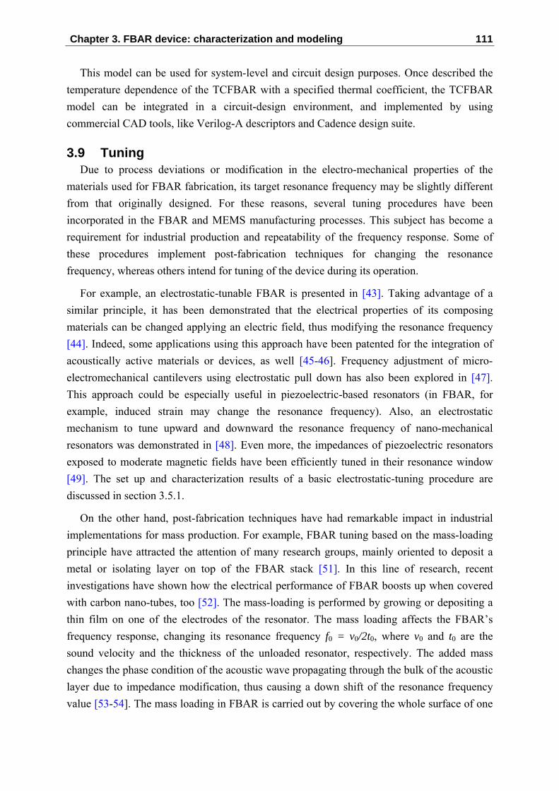
Chapter 3. FBAR device: characterization and modeling 111
This model can be used for system-level and circuit design purposes. Once described the temperature dependence of the TCFBAR with a specified thermal coefficient, the TCFBAR model can be integrated in a circuit-design environment, and implemented by using commercial CAD tools, like Verilog-A descriptors and Cadence design suite.
3.9 Tuning Due to process deviations or modification in the electro-mechanical properties of the
materials used for FBAR fabrication, its target resonance frequency may be slightly different from that originally designed. For these reasons, several tuning procedures have been incorporated in the FBAR and MEMS manufacturing processes. This subject has become a requirement for industrial production and repeatability of the frequency response. Some of these procedures implement post-fabrication techniques for changing the resonance frequency, whereas others intend for tuning of the device during its operation.
For example, an electrostatic-tunable FBAR is presented in [43]. Taking advantage of a similar principle, it has been demonstrated that the electrical properties of its composing materials can be changed applying an electric field, thus modifying the resonance frequency [44]. Indeed, some applications using this approach have been patented for the integration of acoustically active materials or devices, as well [45-46]. Frequency adjustment of micro-electromechanical cantilevers using electrostatic pull down has also been explored in [47]. This approach could be especially useful in piezoelectric-based resonators (in FBAR, for example, induced strain may change the resonance frequency). Also, an electrostatic mechanism to tune upward and downward the resonance frequency of nano-mechanical resonators was demonstrated in [48]. Even more, the impedances of piezoelectric resonators exposed to moderate magnetic fields have been efficiently tuned in their resonance window [49]. The set up and characterization results of a basic electrostatic-tuning procedure are discussed in section 3.5.1.
On the other hand, post-fabrication techniques have had remarkable impact in industrial implementations for mass production. For example, FBAR tuning based on the mass-loading principle have attracted the attention of many research groups, mainly oriented to deposit a metal or isolating layer on top of the FBAR stack [51]. In this line of research, recent investigations have shown how the electrical performance of FBAR boosts up when covered with carbon nano-tubes, too [52]. The mass-loading is performed by growing or depositing a thin film on one of the electrodes of the resonator. The mass loading affects the FBAR’s frequency response, changing its resonance frequency f0 = v0/2t0, where v0 and t0 are the sound velocity and the thickness of the unloaded resonator, respectively. The added mass changes the phase condition of the acoustic wave propagating through the bulk of the acoustic layer due to impedance modification, thus causing a down shift of the resonance frequency value [53-54]. The mass loading in FBAR is carried out by covering the whole surface of one

112 FBAR: fabrication, heterogeneous integration and sensor applications
of the electrodes with a uniform thin-film. The thin-film is deposited by physical vapor deposition (PVD) or grown by means of chemical vapor deposition (CVD) techniques. In section 3.9.2 the uniform-film-based mass-loading of FBARs is described.
New techniques have also demonstrated their suitability for the tuning of micro and nano-sized devices. Thus, the tools implemented in the process are able to perform post-fabrication, localized-mass loading of MEMS resonators. For example, Chiao et al present in [55] a post-packaging tuning process for micro-resonators by pulsed laser deposition (PLD). By adding materials on the surface of the structure, the desired resonant frequency could be achieved. On the other hand, focused-ion-beam (FIB) has become a powerful tool for the post-fabrication of a wide variety of MEMS devices. Subtractive or additive implementations of FIB techniques have enabled the fabrication of three-dimensional structures on a micrometer scale [56-58]. In another example of an elegant FIB application, the milling of optical waveguide MEMS is performed for both characterization and post-fabrication tool of a cantilever sensor [59]. Also, the fabrication process of metal-oxide nano-wires showing gas sensing capabilities being contacted by a dual-beam FIB machine is revealed in [60]. A novel FIB-based technique for tuning of FBARs is introduced in section 3.9.3.
3.9.1 DC tuning The resonance frequency of FBARs can be controlled by changing the electrostatic
configuration of the device, as commented in the above paragraph. By applying a DC-bias voltage to a third electrode of the FBAR, its resonance frequency can be shifted [43]. In this work, a different biasing configuration is proposed: by means of a bias tee, DC and AC voltages are applied to the same FBAR’s electrode, injecting both signals to one of the existing electrodes. Thus, only a single probe is required for application of both DC and AC voltages.
According to this strategy, the measurement setup for DC tuning is depicted in Fig. 3.50 where: (a) the circuit representation; and (b) the physical interconnection of the FBAR to the network analyzer, the DC-power supply, the bias-tee and the probe station are shown (a complete list of the involved instrumentation is provided in Annex VI). As done for the only-AC excitation setup, appropriate calibration standards and routines were initiated in order to compensate the effects of layout-defined transmission line and probing system. The matching impedance of the network analyzer’s ports is 50Ω.

Chapter 3. FBAR device: characterization and modeling 113
Fig. 3.50. Measurement set up for DC tuning using a single electrode for DC+AC voltage supply: (a)
circuit representation, (b) physical connection of the FBAR to the instrumentation and the probe station.
By using the DC-power supply, a DC voltage between 0 and 30 VDC was applied to the first electrode of a testing device, acquiring different measurement data for each bias condition. A resonance-frequency shifting range of 3 MHz was measured and a DC-tuning sensitivity of around 100 kHz/VDC was found. In Fig. 3.51(a), a detailed view of the magnitude of the reflection S11 parameter is observed. In [43], a continuous tuning range of 1.9 MHz for an actuation voltage of 9 VDC was found (resonance frequency of 6.8GHz), thus achieving a tuning sensitivity of 211 kHz/V. Although this value is more than twice of the one obtained by the single-electrode DC+AC tuning method described here, we verified that a minimum tuning range of 3 MHz is possible, making the method suitable for fine tuning in certain RF applications. Furthermore, a high tuning linearity was achieved, as illustrated in the plot of Fig. 3.51(b). In future experiments on DC tuning, the ultimate tuning range and linearity for single-tuning-electrode configurations will be analyzed.

114 FBAR: fabrication, heterogeneous integration and sensor applications
Fig. 3.51. DC tuning in FBARs: (a) magnitude of the S11 parameter for different DC-tuning voltages; (b)
frequency shifting against DC-tuning voltage (tuning sensitivity of 100 kHz/VDC)
3.9.2 Uniform-film deposition Uniform-film deposition can be performed by means of physical vapor deposition (PVD)
or chemical vapor deposition (CVD), or thermal growing techniques. In this work, a thin-film magnesium fluoride (MgF2) layer was deposited on the whole surface of rectangular FBAR –dimensions of 50×70μm2–, by means of physical-vapor-deposition (PVD). The thicknesses of each thin-film deposition were of 2, 5, 10 and 20nm, respectively. This procedure is one implementation of the mass-loading approaches for building tunable FBAR devices found in literature [44-46]. In our implementation, a non-metallic material was deposited. The curves of Fig. 3.52 show experimental data on the resulting frequency shift. Since the PVD process is not easily controllable for film thicknesses under 1nm, it was not possible to deposit MgF2 films with masses as low as for the localized-deposition case.

Chapter 3. FBAR device: characterization and modeling 115
Fig. 3.52. Uniform-film deposition: frequency shifting of the resonance frequency against the amount of
an MgF2 thin-film deposited on top of FBARs
The performance of tuning in micro-electromechanical resonators may be described by one or more metrics. In the case of mass-loading-tuned resonators, mass-responsivity is the main parameter to be considered. The inverse mass-responsivity RM is defined as the number of grams deposited on the device needed to produce a change of 1 Hz in its resonance frequency. In the uniform-film deposition experiments, a highly-linear responsivity value of 1.4×10⁻¹⁷ g/Hz was obtained. In the next section, this result is compared to the responsivity of the FIB-based technique.
3.9.3 Focused-ion-beam (FIB)-assisted tuning technique In this section, we report on an FBAR tuning technique based on focused-ion-beam (FIB),
which has been developed by our group in the context of this work [61]. Deposition of localized mass was performed inside a dual-beam FIB machine, in order to test different possibilities for tuning of the FBAR’s resonance frequency. By localized mass deposition it must be understood deposition of a material whose size is small, compared to the effective resonator’s or electrode surface. In this work, the size of the deposited masses is always less than 0.7% of the electrode’s surface area, this ratio being lower than the 2%-limit established by the Sauerbrey-Lostis model.
For the purpose of deposition, a metalorganic precursor containing Pt is injected close to the FBAR in the sample’s chamber of the FIB machine, and decomposed by the ion beam. By carefully adjusting the dwell time of the ion beam, positioning and current density, this procedure gives rise to the localized deposition of an amorphous compound in the area scanned by the beam. According to Auger Electron Spectroscopy measurements [62], this compound contains C (65%), Pt (27%) and Ga (8%), its mass density being estimated to be equal to 4 g/cm3 [63]. Depending on the size and thickness of the deposited mass the ion current and deposition time need to be adjusted. The schematic diagram of Fig. 3.53 represents the mass deposition procedure: The Pt injector introduces the metalorganic

116 FBAR: fabrication, heterogeneous integration and sensor applications
precursor inside the vacuum chamber, while the same is decomposed by the Ga+ ion-beam scanning the FBAR electrode area. The result is a mass deposited on the top electrode of the FBAR, illustrated in this figure as a square spot. Additionally, the electron beam of the dual beam machines can be used for imaging and calibration purposes without structural damaging of the sample.
Several experiments with a variety of configurations and deposition conditions were carried-out. Thus, the size and location effects of the mass deposition in the mass-loading performance were analyzed. Depositions were done on a group of devices with different layouts, including beams and cantilevers. The SEM images of Fig. 3.54(a) and Fig. 3.54(b) were obtained inside the dual-beam machine and show a rectangular-surface mass deposited on the center of the top Ti/Pt electrode of a rectangular-shaped FBAR. In this figure, the mass has a contact surface of 1.5μm×1.5μm, whereas the FBAR electrode’s surface was of 50μm×50μm. Since the tilting of the electron beam is 52 degrees compared to the ion beam, the vertical scale is compressed as compared to the horizontal one (and this is valid for all the SEM images presented in this paper).
Fig. 3.53. FIB-based tuning set up and procedure: The Pt injector introduces the metalorganic precursor inside the vacuum chamber, whereas the same is decomposed by the Ga+ ion-beam scanning the FBAR
electrode area.

Chapter 3. FBAR device: characterization and modeling 117
Fig. 3.54. FIB-based deposition of a C/Pt/Ga composite on top of FBAR (SEM images): (a) general view;
(b) detailed view of the deposited spot
Examples of other FBAR geometries in which localized tuning of the resonance frequency was performed are shown in the SEM images of Fig. 3.55(a) to Fig. 3.55(c). An FBAR beam with rhomboidal shape (a), a cantilever (b) and a piezoelectric bar (c) illustrate some of the different layout configurations with their corresponding tuning-load deposited on the top electrode.
Since the location and size of the tuning-loads to be deposited give valuable information about the tuning performance, calibration and adjustment of the set-up need to be performed prior to deposition on target FBAR devices. In the following section, some of the main calibration aspects are described, as for example the location, alignment, and verification of the thickness and dimensions of the deposited tuning-load.
Calibration and alignment of deposition The tuning of the FBAR was performed inside a FEI DB Strata235 FIB, a dual beam
instrument. Gallium ion beams, accelerated at 30 kV, are able to promote the decomposition of the precursor gas crossing their path, promoting ion-assisted deposition (IACVD). As a dual-beam system, it combines scanning electron microscopy (SEM) and FIB in one machine, able to assist deposition of materials with nanometer precision. Careful alignment of electron and ion beams is fundamental for successful supervision and deposition results and this has to be performed in a region far from the FBAR structure.
Fig. 3.55. Examples of other FBAR geometries in which localized tuning of the resonance frequency was
performed: (a) rhomboidal-shaped; (b) cantilever; (c) piezoelectric bar

118 FBAR: fabrication, heterogeneous integration and sensor applications
Some undesired effects, like charging of the sample's surface, may occur during deposition, thus causing the ion beam to be shifted away from the alignment point previously selected. Although such shifting should not significantly affect the performance of small-sized mass deposition on the typical FBAR device, it could cause the tuning-load to be deposited out of the surface of narrower devices. In this way, the execution of a calibration procedure helps the improvement of the deposition accuracy. Calibration is also important for analyzing the performance of the frequency tuning of the FBAR. Two aspects mainly influence this performance: first, the size of the deposited mass; and second, the collateral effects of the ion beam in the sample’s surface (residual etching or deposition may occur in the surroundings of the target area). This could happen due to inappropriate selection of the ion-current or scanning conditions.
In this way, the calibration initiates when a test sample is brought into the FIB’s machine chamber and located at a pre-specified distance to the objective lens of the electron-beam. Then, a reference point in the scanning area of the electron-beam is selected, and alignment of the ion-beam is done in order to take an image of the selected point. The calibration sample should have a surface with the same layout and structure of the target-deposition sample. Next, mass deposition is performed on this surface. When the deposition is completed, milling of the closest vicinity of the deposited load is performed by means of the ion-beam. This procedure allows the cross-sectional observation of the deposited mass structure and its dimensions. Appropriate milling succeeds in cross-cutting the structure around the deposited spot, in order to observe the FBAR-layered configuration by means of SEM imaging. Previous knowledge of the FBAR’s structure composition and of the deposition set-up allows the evaluation of the effects of the first-calibration deposition. If one layer appears to be thinner –especially around or below the deposited tuning-load– or if the deposited mass reveals to be smaller or thinner than expected, the set-up needs to be re-adjusted.
The SEM images in Fig. 3.56(a) and Fig. 3.56(b) show two examples of calibration routines with the aim of set-up of the ion-beam. First, in Fig. 3.56(a) the cross-cutting view of a square-shaped load is observed. Although a cubic shape was expected, some lateral drifting of the ion-beam caused the final deposition to have a conformal shape. This issue should be corrected prior to final-device deposition, or a new deposition carried out in a different device. The second example is shown in Fig. 3.56(b), where the layered structure of the FBAR is appreciated. Here, milling of the device allows the evaluation of the quality and thickness of each layer in the FBAR’s stack. Applying a correction factor of the vertical scale –due to the set-up tilting of the electron-beam–the thickness of the composing materials can be measured (given the topographic scale, annotated in the image).

Chapter 3. FBAR device: characterization and modeling 119
Fig. 3.56. Two examples of calibration routines of the ion-beam: (a) Deposition and milling of a square-
shaped spot, in which the conformal configuration in the vertical axis is observed. (b) Milling of the FBAR’s layered structure. In considering the scale and the 52-degree tilting of the e-beam, the thickness
of the AlN is determined to be of 1μm.
In summary, the goals of the calibration are accomplished when the surface of the calibration-sample is not affected after the deposition and if the size, distribution and location of the deposited-mass are according to the desired configuration for the target-device. At this point, the final-device deposition can be initiated. Accepting that the chosen FIB’s configuration enables the set-up for reliable mass deposition, the results of the ion-assisted depositions can be analyzed. In such a way, the incidence of electrical and scanning conditions in both tuning and FIB-machine utilization performance is discussed in the following sections.
Electrical and scanning conditions for practical processing time The current-density and scanning area of the ion-beam (i-beam) are the main parameters
determining the processing time of the sample inside the FIB’s chamber, for mass deposition or milling, as well. Hence, these parameters should be configured depending on the size and thickness of the processing area of the FBAR’s surface. For example, mass deposition on the sample FBAR shown in Fig. 3.54 took 3 minutes and 28 seconds to be completed. Having a thickness of 400nm and a contact area of 1.5μm×1.5μm, the mass was deposited with an i-beam current of 10 pA (current density of 4.4 pA/μm2). As long as deposition or milling can be controlled either by time or thickness, the size of the mass or milling-hole establishes the most convenient choice for the process: if the thickness of the tuning-load is in the range of units or tens of nanometer, a time-driven deposition is a more practical configuration and is the preferred option to obtain a mass-thickness closer to the expected value. On the other hand, if the thickness is in the hundreds of nanometer and the lateral size of the deposition/milling is in the tens of micrometer, the i-beam current needs to be incremented at least one order of magnitude, in order to complete the deposition in practical time intervals. For a second testing FBAR, in which the tuning-load had dimensions of 20μm×20μm×100nm, a 300pA i-beam current was chosen in order to use roughly the same

120 FBAR: fabrication, heterogeneous integration and sensor applications
deposition time (equivalent to a current density of 0.75 pA/μm2). In both cases the FBARs had a rectangular shape with electrode surface area of 50×70μm2.
Regarding the experiments to study the i-beam scanning conditions, identical masses were deposited on three rectangular-shaped resonators with electrode area of 50×70μm2. In this way, each device was loaded with a tuning-load of nominal mass of 8.1×10⁻¹² g. Different i-beam currents and deposition times were investigated, in order to analyze their incidence in the electrical performance of the tuning. In Table 3.8 the relationship between the FIB-deposition conditions, the deposited load dimensions and mass, and the measured change in the resonance frequency of FBARs is shown. As it can be appreciated, different i-beam set-up conditions lead to different frequency shifts.
These differences may be explained by two characteristics of the set-up: a) the different density of the mass for different current-density depositions; and b) more current-fluctuation and relative bigger variance of the i-beam current for the low-current-density case. The mass-density was previously characterized for standard-deposition conditions. Thus, statistical variation of the i-beam current and the high frequency sensitivity of FBAR may lead to misinterpretation of the frequency shift (probably due to higher or lower mass density of the C/Pt/Ga compound). On the other hand, the current fluctuations for the low current-density values employed here (10 pA) have been estimated as being around 4pA. However, these pA-valued fluctuations are only a small fraction of the nominal value for high-currents (hundreds of pA).
A careful record of the current fluctuations during deposition for different i-beam current configurations will allow us future verification of these assumptions. In the following section we show how different i-beam set-up conditions may lead to milling –instead of deposition– of the FBAR structure.
Table 3.8. Mass-deposition and tuning results obtained for different ion-beam configurations.
Device/ FIB set-up
Loading dimensions
(μm×μm ×nm)
Current density
(pA/μm2)
Mass (g,
calculated)
Frequency shift (Hz)
1 Current: 10pA– Time: 5’28’’
10×10×20 0.1 8.1×10⁻¹² 2.2×10⁶
2 Current: 300pA– Time: 10.9’’
10×10×20 3 8.1×10⁻¹² 1.6×10⁶
Milling of FBAR as another FIB-tuning procedure
At this point, we have proposed a mass-loading tuning procedure of the FBAR’s top electrode. In this procedure, the ion-beam performs deposition of the C/Pt/Ga composite on the FBAR’s surface. However, under certain i-beam set-up conditions, milling –etching– of the device structure can be performed, de-loading the resonator. Typically etching is obtained for current densities above about pA/μm2, but other considerations, as scanning speed, also

Chapter 3. FBAR device: characterization and modeling 121
influences the process. While the resonance frequency may be down-shifted by means of the mass-loading procedure, with the mass de-loading this frequency is expected to be up-shifted. Since the localized etching of the top electrode modifies the structure of the device, we can suppose a change of the mode-shaping of the resonance, too. Thus, it is important to understand the interaction between de-loading, frequency tuning and resonance’s mode shaping. The SEM image of Fig. 3.57 shows a region of a “de-loaded” FBAR, in which the Ti/Pt top electrode has been locally milled by the i-beam. In this image the underlying AlN layer is observed in the milled area. A fully-milled device was previously shown in the image of Fig. 3.56(b), where the top-to-bottom Ti/Pt/AlN/Ti/Pt structure can be observed.
The FIB-assisted milling of FBAR may also find application in post-fabrication releasing of partially-released devices. This can take place if the micro-machining time was not enough to completely release-off the subjacent silicon substrate –or sacrificial layer, if provided–. In this application, milling of the non-released region of the resonator provides electrical isolation between the released and the non-released areas. For this purpose, first we need to know the boundaries of the etched and non-etched areas underneath the device. Once known the size of the released FBAR volume, i-beam milling will assist in the final releasing of the resonator.
Exploratory milling of a FBAR device was carried out on a rhomboidal resonator, in order to determine the under-etching rate of the micro-machining process. The results are shown in the SEM image of Fig. 3.58(a). Here, both the non-released and released regions can be observed. Due to incomplete etching, the silicon substrate still remains underneath the FBAR structure (right side of Fig. 3.58(a)). With this information, a second experiment was performed on another device with rhomboidal shape, which is shown in the SEM image of Fig. 3.58(b). Here, the rectangular-shaped frame isolates the areas inside and outside the milling perimeter, both mechanically and electrically (the volume inside the frame is actually isolated, the effective device being the volume outside of the frame).
Fig. 3.57. Illustration of the milling-based de-loading concept: Ion-assisted etching locally removes the
Ti/Pt top electrode of FBAR (the square-shaped etching allows observation of the AlN layer)

122 FBAR: fabrication, heterogeneous integration and sensor applications
Fig. 3.58. Post-fabrication release of FBAR: (a) exploratory milling for determining the released and non-release device boundaries. (b) Rectangular milling practiced on a rhomboidal device (isolation of the inner
region of rectangle is achieved)
Based on the same principle, we can change the shape of the resonance modes of the FBAR by means of transversal milling of the structure. In this way, the mode shapes of the FBAR are engineering after fabrication, given previous knowledge of the resonance modes and appropriate milling of the structure. This is useful in devices presenting a high number of spurious resonance modes. To illustrate this concept, a third milling-experiment was carried out in the rectangular FBAR shown in the SEM image of Fig. 3.59(a). Suppression of the spurious modes was achieved by means of transversal cuts of the layered FBAR structure, as observed in the image.
Electrical characterization of the magnitude of the S21 parameter, before and after milling, demonstrates how rippling and some resonance modes are no longer visible after the FIB processing (curves of Fig. 3.59(b)). However, it can also be appreciated how the energy of the resonance peaks diminishes, probably due to residual –and undesired– inhibition of the main resonance modes. Looking at the curves, the new resonance shape coincides with the shape and frequency of smaller modes observed in the non-milled device. These modes were superposed to the main and to other small spurious modes before the milling, and would be now enhanced due to the i-beam processing. Of course, systematic engineering of the mode-shape requires finite-element analysis, the examples presented here being an example of the potential of this tool for mode shaping.
Chapter 3. FBAR device: characterization and modeling 123
Fig. 3.59. FIB-based engineering of mode shaping in FBAR: (a) SEM image of FBAR with transversal cuttings (intended for suppression of spurious modes). (b) Magnitude of S21 transmission parameter,
before –dotted line– and after FIB-assisted milling (ripple and some spurious modes disappeared for the after-FIB case, continuous line)
Frequency-tuning sensitivity and responsivity First, i-beam deposition of the C/Pt/Ga composite was performed on the geometric center
of the top electrode of a group of rectangular resonators with electrode area of 50×70μm2. The squared-shaped localized-masses had a size of 1.5×1.5 μm2 and different thicknesses to change the amount of mass; in the range of 9.0×10⁻¹⁵ g to 3.6×10⁻¹² g. The frequency shift against the amount of deposited mass is shown in the plot of Fig. 3.60 (the x-axis is represented in log-scale, due to the wide range of deposited masses). Regarding these results the responsivity may be calculated, its average value being 7.4×10⁻¹⁹ g/Hz. This value is competitive with respect to other NEMS technologies previously reported [64-66].

124 FBAR: fabrication, heterogeneous integration and sensor applications
Fig. 3.60. Frequency shift of the resonance frequency against the amount of tuning-load: (a) detailed
sensitivity plot; (b) FIB-tuning performance compared to uniform-film deposition
Thus, we have extrapolated the linear fit of the uniform-film case to illustrate how the responsivity of the localized-deposition is better than for the uniform-film case. In this way, the extrapolated curve shows that the frequency change is between one and three orders of magnitude higher for the i-beam tuning procedure.
Quality factor The quality factor (Q) of the resonator mainly determines the ultimate mass-sensitivity of
the same, since it is related with the minimum change of frequency. In this sense, the Q factor is an important issue to be considered in mass-loading-based tuning of FBAR. During deposition, the i-beam might induce heat damages in the resonator’s structure, due to possible heating of the materials, thus reducing its Q factor. For this reason, additional experiments were carried out, in order to evaluate the possible incidence of the i-beam in the physical properties and electrical response of the FBAR.

Chapter 3. FBAR device: characterization and modeling 125
With the aim of verification of this issue, additional experiments and measurements were done on selected devices. First, we took a group of resonators and measured the electrical response, by evaluating the magnitude of the S21 parameter and of the Q factor. Next, we introduced each of the FBARs into the FIB chamber and performed i-beam imaging or small-mass deposition on them. Finally, we characterized again the S21 and the Q factor values.
The results proved that no appreciable electro-mechanical modification in the behavior of the FBAR for the localized-mass deposition occurred, since none of the electrical parameters of the samples were affected. The quality factor of all the devices was around 500 before and after the i-beam operation. The plot of Fig. 3.61 compares the magnitude of the S21 parameter before and after i-beam imaging practiced on a sample FBAR. The S parameters and the quality factor remained constant in both cases.
Some explanations can be given to this fact. First, not enough heating of the structure occurs to modify the piezoelectric properties of the AlN. Also related to this hypothesis, the longitudinal resonance mode and the reduced size of the mass –compared to the FBAR– inhibits to a great extent the mass-related damping. As a difference to a recent work, in which Pt was deposited on a 13 μm × 5 μm surface area at the free end of 3C silicon carbide (SiC) and polysilicon cantilever resonators [67], the FBAR works in a bulk, longitudinal resonance mode (in low-frequency mechanical resonance modes, as the vibrating cantilever case, the electro-mechanical damping of the deposited mass is more important in the Q factor behavior). Also, the mass is deposited on top of the Pt layer of the FBAR, and no interaction occurs between the i-beam and the AlN, since it is covered by the Pt-made top electrode. In this case, the AlN quality mainly determines the Q factor of the FBAR.
Fig. 3.61. S21 magnitude of FBAR before and after i-beam operation (no mass deposition, only i-beam
imaging). No significant change of the response is observed

126 FBAR: fabrication, heterogeneous integration and sensor applications
3.10 Summary In this chapter, the main characterization results addressed by this thesis have been
presented:
• Low-frequency and high-frequency characterization of FBARs was performed. The
characterization set up was described and layout considerations affecting the
performance of FBARs commented. Based on characterization results, the main
electro-mechanical constants of the AlN were extracted. The quality factor and
electro-mechanical coupling coefficients were also evaluated, and the process
deviations and time-frequency stability of the devices analyzed.
• An algorithm implementing automatic parameter extraction in FBAR was described.
By means of this algorithm, on-wafer calibration may be avoided thus achieving
instantaneous de-embedding of the resonator's equivalent-circuit parameters.
• Temperature-coefficients of fabricated FBARs were evaluated, and a temperature-
compensation strategy implemented. TCFBARs were designed and fabricated, and
their TCF characterized, obtaining compensation respect to non-compensated FBARs.
Further TCFBAR designs and experiments will be carried out in the future.
• The tuning of FBAR devices by means of ion-assisted deposition using a FIB machine
has been demonstrated. Different i-beam-tuning procedures, including deposition and
milling of the FBAR; were described. Also, comparison of the i-beam and uniform-
film tuning cases was done, finding out that the tuning procedure proposed in this
work exhibits improved responsivity performance, compared to uniform-film
deposition. With the i-beam tuning procedure, an average responsivity of 7.4×10⁻¹⁹
g/Hz was achieved, which is between one and two orders of magnitude better than for
the thin-film deposition case. Additionally, the effects of different mass-loading
configurations in the tuning performance were discussed. The possible influence of the
i-beam in the physical structure and electrical response of the FBAR was also
analyzed. No significant variation in the Q factor or the S parameters was observed.
Although we have been already studying main aspects of localized-tuning of FBAR by
means of ion-beam-assisted deposition, several challenges should be faced on. Future
developments of this work should allow us studying the resonance-mode shaping
effects in the mass responsivity of the tuning.

Chapter 3. FBAR device: characterization and modeling 127
References 1 W.A. Davis and K.K. Agarwal, “Radio Frequency Circuit Design”. John Wiley & Sons, Canada.
2001.
2 Q. Su, P. Kirby, E. Komuro, M. Imura, Q. Zhang, and R. Whatmore, “Thin-film bulk acoustic resonators and filters using ZnO and lead–zirconium–titanate thin films”, IEEE T. Microw. Theory Tech. 49 (2001) 769-778.
3 Rogers Corporation, “RO3000 Series High Frequency Circuit Materials”. Available on-line (accessed November 2007): http://www.rogerscorporation.com/mwu/pdf/3000data.pdf
4 A. Link, E. Schmidhammer, H. Heinze, M. Mayer, M. Schmiedgen, B. Bader, K. Wagner, and R. Weigel, "Suppression of spurious modes in mirror-type thin film BAW resonators using an appropriate shape of the active area", in Proc. IEEE Intl. Ultrason. Symp. 2005, Sept. 18-21 2005, Rotterdam, The Netherlands, 2, 1179-1182.
5 Y.W. Lin, S. Lee, S.S. Li, Y. Xie, Z. Ren, and C.T.-C. Nguyen, “Series-resonant VHF micromechanical resonator reference oscillators”, IEEE J. Solid State Circuits 39 (2004) 2477-2491.
6 ANSI/IEEE Std. 176-1987, “IEEE Standard on Piezoelectricity”. The Institute of Electrical and Electronics Engineers, Inc, 1988, New York, NY, USA.
7 H. Hasegawa, M. Furukawa, and H. Yanai, “Properties of microstrip line on Si-SiO2 system”, IEEE T. Microwave Theory Techniques 19 (2001) 869-881.
8 T.P. Alexander, T.R. Bukowski, D.R. Uhlmann, G. Teowee, K.C. McCarthy, J. Dawley, and B.J.J. Zelinski, “Dielectric Properties of Sol-Gel Derived ZnO Thin Films”, in Proc. Tenth IEEE International Symposium on Applications of Ferroelectrics Ferroelectrics ISAF’96, 18-21 Aug. 1996, East Brunswick NJ, USA, 2, 585-588.
9 T. Makkonen, T. Pensala, J. Vartiainen, J.V. Knuuttila, J. Kaitila, and M.M. Salomaa, “Estimating materials parameters in thin-film BAW resonators using measured dispersion curves”, IEEE T. Ultrason. Ferroelectr. Freq. Control 51 (2004) 42-51.
10 M. Ylilammi, J. Ella, M. Partanen, and J. Kaitila, “Thin Film Bulk Acoustic Wave Filter”, IEEE T. Ultrason. Ferroelectr. Freq. Control 49 (2002) 535-539.
11 B. Razhavi, RF microelectronics, Prentice Hall PTR, Upper Saddle River, NJ, USA, 1998.
12 J. Kaitila, M. Ylilammi, Juha Ellä and R. Aigner, “Spurious resonance free bulk acoustic wave resonators”, in Proc. IEEE Intl. Ultrason. Symp. 2003, 5-8 Oct. 2003, Honolulu, Hawaii, USA, 84-87.
13 A. Sanz-Hervás, M. Clement, E. Iborra, L. Vergara, J. Olivares, and J. Sangrador, “Degradation of the piezoelectric response of sputtered c-axis AlN thin films with traces of non-(0002) x-ray diffraction peaks”, Appl. Phys. Lett. 88 (2006) 161915.
14 A.L. Kholkin, A.K. Tagantsev, K.G. Brooks, D.V. Taylor, and N. Setter, “Piezoelectric characterization of Pb(Zr,Ti)O3 thin films by interferometric technique”, in Proc. Tenth IEEE International Symposium on Applications of Ferroelectrics Ferroelectrics ISAF’96, 18-21 Aug. 1996, East Brunswick NJ, USA, 1, 351-354.
15 K. Tsubouchi, K. Sugai, N. Mikoshiba, “AlN material constants evaluation and SAW properties on AlN/Al2O3 amd AlN/Si”, in Proc. IEEE Intl. Ultrason. Symp. 1981, 14-16 Oct. 1981, Chicago IL, USA, 1, 375-380.
16 D. Berlincourt, H. Jaffe, and L.R. Shiozawa, “Electroelastic properties of the sulfides, selenides,and tellurides of zinc and cadmium”, Phys. Rev. 129 (1963) 1009-1017.
17 W..P. Mason, Electromechanical Transducers and Wave Filters, Princeton, NJ, Van Nostrand, 1948
128 FBAR: fabrication, heterogeneous integration and sensor applications
18 W.P. Mason, Physical Acoustics and the Properties of Solids, D. Van Nostrand Co., Princeton, NJ, 1958
19 R. Krimholtz, D.A. Leedom, and G.L. Matthaei, “New Equivalent Circuit for Elementary Piezoelectric Transducers”, Electron. Lett. 6 (1970) 398-399.
20 D. Rosén, J. Bjursttröm, and I. Katardjiev, “Suppression of spurious lateral modes in thickness-excited FBAR resonators”, IEEE T. Ultrason. Ferroelectr. Freq. Control 52 (2005) 1189-1192.
21 Y.-D. Kim, K.-H. Sunwoo, S.-C. Sul, J.-H. Lee, D.-H. Kim, I.-S. Song, S.-H. Choa, and J.-G. Yook, “Highly Miniaturized RF Bandpass Filter Based on Thin-Film Bulk Acoustic-Wave Resonator for 5-GHz-Band Application”, IEEE T. Microw. Theory Tech. 54 (2006) 1218-1228.
22 G.G. Fattinger, S. Marksteiner, J. Kaitila, and R. Aigner, “Optimization of acoustic dispersion for high performance thin film BAW resonators”, in Proc. IEEE Intl. Ultrason. Symp. 2005, Sept. 18-21 2005, Rotterdam, The Netherlands, 1, 1175 - 1178.
23 Avago Technologies. Available on-line (accesed November 2007): http://www.avagotech.com/products/rf_for_mobile%2C_wlan%2C_mmw/mobile_filtering/
24 Infineon Technologies. Available on-line (accesed November 2007): http://www.infineon.com/cms/en/product/chanel.html?channel=ff80808112ab681d0112ab6ab20605d5
25 R. Ruby, P. Bradley, J. Larson III, Y. Oshmyanski, and D. Figueredo, “Ultra-Miniature High-Q Filters and Duplexers Using FBAR Technology”, in IEEE Intl. Solid-State Circuits Conf. Dig. of Tech. Papers, Feb. 5-7 2001, San Francisco, CA, USA, 120-121.
26 K.M. Lakin, J.R. Belsick, J.P. McDonald, K.T. McCarron, and C.W. Andrus, "Bulk Acoustic Wave Resonators And Filters For Applications Above 2 GHz", in IEEE International Microwave Symp. MTT-S 2002 Digest of Tech. Papers, Jun. 3-7 2002, Seattle, WA, USA, 3, 1487-1490.
27 K.-W. Kim, M.-G. Gu, J.-G. Yook, and H.-K. Park, “Resonator size effects on the TFBAR ladder filter performance”, IEEE Microw. Wirel. Compon. Lett. vol. 13, no. 8, August 2003, pp. 335-337.
28 R. Ruby, “Review and comparison of Bulk Acoustic Wave FBAR and SMR technology”, in Proc. IEEE Intl. Ultrason. Symp. 2007, 28-31 October 2007, New York City, USA.
29 J. Larson III, P. Bradley, S. Wartenberg, and R. Ruby, Modified Butterworth-Van Dyke Circuit for FBAR Resonators and Automated Measurement System, in Proc. IEEE Intl. Ultrason. Symp. 2000, Oct. 22-25 2000, San Juan-Puerto Rico, 863-868.
30 J. Lee, J. Jung, J. Park, and H. Kim, “Extraction of Material Parameters in Film Bulk Acoustic Resonators (FBAR) Using Genetic Algorithm”, IEEE Electron Device Lett. 25 (2004) 67-69.
31 W. Wheless and D. Kajfez, “Microwave resonator circuit model from measured data fitting”, in Proc. IEEE International Microwave Symp. MTT-S 1986 Digest of Tech. Papers, Jun. 2-4 1986, Baltimore MD, USA, 681-684.
32 H. Kondoh, “An accurate FET modeling from measured S-parameters”, in Proc. IEEE International Microwave Symp. MTT-S 1986 Digest of Tech. Papers, Jun. 2-4 1986, Baltimore MD, USA, 377-380.
33 G. Kompa and M. Novotny, “Highly consistent FET model parameter extraction based on broadband S-parameter measurements”, in Proc. IEEE International Microwave Symp. MTT-S 1992 Digest of Tech. Papers, Jun. 1-5 1992, Albuquerque NM, USA, 293-296.
34 F. Seyfert, L. Baratchart, J.-P. Marmorat, S. Bila, and J. Sombrin, “Extraction of coupling parameters for microwave filters: determination of a stable rational model from scattering data”, in Proc. IEEE International Microwave Symp. MTT-S 1992 Digest of Tech. Papers, Jun. 8-13 2003, Philadelphia PA, USA, 25-28.

Chapter 3. FBAR device: characterization and modeling 129
35 H. Campanella, P. Nouet, P. de Paco, A. Uranga, N. Barniol, and J. Esteve. “Automated on-wafer extraction of equivalent-circuit parameters in thin-film bulk acoustic wave resonators (FBAR) and substrate”, Microwave Optical Tech. Lett. 50 (2008) 4-7.
36 H. Campanella, J. Esteve, A. Uranga, P. De Paco, N. Barniol, and P. Nouet, “Instantaneous de-embedding of the on-wafer equivalent-circuit parameters of acoustic resonator (FBAR) for integrated circuit applications”. In Proc. 20th Symposium on Integrated Circuits and Systems Design SBCCI’07, Sept. 3–6, 2007, Rio de Janeiro, Brazil, 212-217.
37 H. Campanella, P. Nouet, P. de Paco, A. Uranga, N. Barniol, and J. Esteve. “Automated on-wafer characterization in micro-machined resonators: towards an integrated test vehicle for bulk acoustic wave resonators (FBAR)”. In Proc. IEEE Intl. Conf. Microelectronic Test Structures ICMTS 2007, March 19-22, 2007, Tokyo, Japan, 157-161.
38 B.D. Andersen, and N.A. Belkerdid, “Measurement sensitivity analysis of one port BAW resonators”, in Proc. 50th IEEE International Frequency Control Symposium 1996, 5-7 June 1996, Honolulu HW, USA, 357-362.
39 S. Gribaldo, C. Chay, E. Tournier, O. Llopis, “Experimental study of phase noise in FBAR resonators”, IEEE T. Ultrasonics, Ferroelectrics, Freq. Control. 53 (2006) 1982-1986.
40 F. Vanhelmont, P. Philippe, A.B.M. Jansman, R.F. Milsom, J.J.M. Ruigrok, and A. Oruk, “A 2GHz reference oscillator incorporating a temperature compensated BAW resonator”, in Proc. IEEE Intl. Ultrason. Symp. 2006, Oct. 3-6 2006, Vancouver, Canada, 333-336.
41 J.D. Larson III, “Method of making an acoustic wave resonator”, U.S. patent no. 6,874,212, Apr. 2005.
42 T.Karaki and M.Adachi (Toyma Prefecture University), and M. Furuhata (SEIKO EPSON Corp.), private communication, 2007.
43 W. Pan, P. Soussan, B. Nauwelaers, and H.A.C. Tilmans, “A surface micromachined electrostatically tunable film bulk acoustic resonator”, Sens. Actuator A-Phys. 126 (2006) 436-446.
44 M.J. Lancaster, J. Powell, and A. Porch, “Thin-film ferroelectric microwave devices”, Supercond. Sci. Technol. 11 (1998) 1323-1334
45 J. Ella, “Device incorporating a tunable thin film bulk acoustic resonator for performing amplitude and phase modulation” US Patent 5714917, 1998.
46 C. Korden, T. Ostertag, and W. Ruile “Component having an acoustically active material for tuning during operation”, US patent 6847271, 2005.
47 S.M.M. Kafumbe, J.S. Burdess, and A.J. Harris “Frequency adjustment of microelectromechanical cantilevers using electrostatic pull down” J. Micromech. Microeng. 15 (2005) 1033-1039
48 I. Kozinsky, H.W.Ch. Postma, I. Bargatin, and M.L. Roukes “Tuning nonlinearity, dynamic range, and frequency of nanomechanical resonators”, Appl. Phys. Lett. 88 (2006) 253101
49 M. Maglione, W Zhu, and Z.H. Wang, “Evidence of a strong magnetic effect on the impedance of integrated piezoelectric resonators” Appl. Phys. Lett. 87 (2005) 092904
50 R. C. Ruby and P. P. Merchant, “Tunable thin film acoustic resonators and method for making the same”, U.S. Patent No. 5587620, 24 Dec. 1996.
51 M. A. Ylilammi, “Method for performing on-wafer tuning of thin film bulk acoustic wave resonators (FBARS)”, U.S. Patent No. 6051907, 18 Apr. 2000.
52 M. Dragoman, A. Muller, D. Neculoiu, D. Vasilache, G. Konstantinidis, K. Grenier, D. Dubuc, L. Bary, R. Plana, and E. Flahautn, “High performance thin film bulk acoustic resonator covered with carbon nanotubes”, Appl. Phys. Lett. 89 (2006) 143122
130 FBAR: fabrication, heterogeneous integration and sensor applications
53 G.Z. Sauerbrey, “Verwendung von Schwingquarzen zur Wägung dünner Schichten und Microwägung”, Z. Phys. 155 (1959) 206-222.
54 P. Lostis, Rev. Opt., Theor. Instrum. 38 (1959) 1.
55 M. Chiao and L. Lin “Post-packaging frequency tuning of microresonators by pulsed laser deposition”, J. Micromech. Microeng. 14 (2004) 1742-1747
56 T. Fujii, K. Iwasaki, M. Munekane, T. Takeuchi, M. Hasuda, T. Asahata, M. Kiyohara, T. Kogure, Y. Kijima, and T. Kaito, “A nanofactory by focused ion beam”, J. Micromech. Microeng. 15 (2005) S286-291.
57 S. Reyntjens and R. Puers, “Focused ion beam induced deposition: fabrication of three-dimensional microstructures and Young's modulus of the deposited material” J. Micromech. Microeng. 10 (2000) 181-188.
58 S. Reyntjens and R. Puers, “A review of focused ion beam applications in microsystem technology”, J. Micromech. Microeng. 11 (2001) 287-300.
59 M.W. Pruessner, N. Siwak, K. Amarnath, S. Kanakaraju, W.-H. Chuang, and R. Ghodssi, “End-coupled optical waveguide MEMS devices in the indium phosphide material system”, J. Micromech. Microeng. 16 (2006) 832-842.
60 F. Hernández-Ramírez, A. Tarancón, O. Casals, J. Rodríguez, A. Romano-Rodríguez, J.R. Morante, S. Barth, S. Mathur, T.Y. Choi, D. Poulikakos, V. Callegari, and P.M. Nellen, “Fabrication and electrical characterization of circuits based on individual tin oxide nanowires”, Nanotechnol. 17 (2006) 5577-5583.
61 H. Campanella, F. Hernández-Ramírez, A. Romano-Rodríguez, J. Montserrat, A. Uranga, N. Barniol, and J. Esteve, “Focused-ion-beam-assisted tuning of thin-film bulk acoustic wave resonators (FBAR)”, J. Micromech. Microeng. 17 (2007) 2380-2389.
62 A. Vilà, F. Hernández-Ramírez, J. Rodríguez, O. Casals, A. Romano-Rodríguez, J.R. Morante, and M. Abid, “Fabrication of metallic contacts to nanometer-sized materials using a focused ion beam (FIB)”, Mater. Sci. Eng. C 26 (2006) 1063-1066.
63 H. Mulders (FEI Company), private communication.
64 E. Forsen, G. Abadal, S. Ghatnekar-Nilsson, J. Teva, J. Verd, R. Sandberg, W. Svendsen, F. Perez-Murano, J. Esteve, E. Figueras, F. Campabadal, L. Montelius, N. Barniol, and A. Boisen, “Ultrasensitive mass sensor fully integrated with complementary metal-oxide-semiconductor circuitry”, Appl. Phys. Lett. 87 (2005) 043507-1-3.
65 K.L. Ekinci, X.M.H. Huang, and M.L. Roukes, “Ultrasensitive nanoelectromechanical mass detection”, Appl. Phys. Lett. 84 (2004) 4469-4471.
66 B. Ilic, H.G. Craighead, S. Krylov, W. Senaratne, C. Ober, and P. Neuzil, “Attogram detection using nanoelectromechanical oscillators”, J. of Appl. Phys. 95 (2004) 3694-3703.
67 S. Enderling, J. Hedley, L. Jiang, R. Cheung, C. Zorman, M. Mehreganym and A.J. Walton, “Characterization of frequency tuning using focused ion beam platinum deposition”, J. Micromech. Microeng. 17 (2007) 213–219.

Chapter 3. FBAR device: characterization and modeling 131

CHAPTER 4
Heterogeneous integration of FBAR with CMOS technologies
Nowadays, heterogeneous integration is considered as a key strategy towards the
realization of the System-on-Chip (SoC) and System-on-a-Package (SoP) concepts. Heterogeneous integration designates technologies that can be integrated on one platform device, enabling the fabrication and assembly of complete electronic subsystems from components fabricated by a range of processes such as MEMS devices, SOI/CMOS mixed signal ASICs, micro scale passive components and micro power systems.
This chapter presents a method for performing heterogeneous integration of FBARs with CMOS substrates, as a technology path for accomplishing the demanding requirements of integration and process compatibility of FBAR with CMOS integrated-circuit technologies. Concept, fabrication process and realization, and characterization results are discussed. Different technologies including surface micromachining, flip-chip, and multi-chip-module, among others, have been implemented to accomplish wafer-level-transfer of the FBAR to the CMOS substrate. The heterogeneous integration approach offers many advantages, compared to monolithic or hybrid integration, among them: 1. Compatibility: The integration is performed with independence of the FBAR or CMOS fabrication technologies and their constraints and process requirements. 2. Versatility: This technology is not limited to the CMOS integration of FBAR devices and its principles may be applied to other suitable MEMS devices. 3. Lower process complexity: The micromachining-driven FBAR releasing can be performed as part of the integration process, reducing the manufacturing time and simplifying the complexity of the technology. These features and the results of electrical characterization are discussed along this chapter.
The main contribution of this method is an FBAR exhibiting a 3D-structure, which is transferred to the CMOS circuit by implementing a heterogeneous integration method. Concept demonstration was achieved by integrating FBARs with two different standard CMOS technologies: the in-house CNM25 and the commercial Austria Micro System’s AMS035 substrates.
4.1 Introduction Various FBAR-to-CMOS integration technologies have been developed during the past
few years, some of the most relevant being: a) The hybrid integration by wire-bonding or flip-

134 FBAR: fabrication, heterogeneous integration and sensor applications
chip of the FBAR and the CMOS circuit [1, 2]; and c) the monolithic integration by manufacturing of the FBAR and the circuit on the same CMOS substrate [3]. Additionally, the packaging technology of the FBAR, or any similar MEMS device, by means of thru-hole or via-hole interconnection has also been developed [4]; Although no FBAR-CMOS implementation has already been disclosed, heterogeneous integration has been demonstrated in other MEMS-CMOS systems [5].
FBAR-to-CMOS integration has stimulated the conception of integrated applications in which FBAR is a key component and whose IC integration is a requirement for proper functionality of the system. Different integration strategies have been investigated, hybrid and monolithic methods among them. By means of hybrid integration, two systems located in separated substrates are typically integrated by wire-bonding or flip-chip of the involved devices. Example of this integration approach is the oscillator presented in [1], where the FBAR performs the crystal-like functionality in the system. In the second approach, monolithic integration of FBARs with CMOS substrates is carried out. In the typical conception, the FBAR is placed above the circuit, in order to save die area. This approach was disclosed in 1993 [6], even a system integrating FBAR and radio circuitry was conceived in 2001 [7]. However, it was not as late as 2005 when the first monolithic FBAR-above-IC systems were demonstrated [3]. The interest for monolithic integration of FBAR has not been limited to fully-active ICs, but also for passive components like CMOS inductors [8]. Other MEMS, NEMS and SAW integrated resonators have been demonstrated, as well [9-11].
To date, wire-bonding, flip-chip and monolithic approaches have been mainstream technologies in MEMS and FBAR integration. More recently, however, heterogeneous integration has begun to be considered as a key strategy towards the realization of the System-on-Chip (SoC) – System-on-a-Package (SoP) concept. Heterogeneous integration designates technologies that can be integrated on one platform device. The concept of “Heterogeneous Integration” enables the fabrication and assembly of complete electronic subsystems from components fabricated by a range of processes. Included in such a system could be MEMS devices, SOI/CMOS mixed signal ASICs, micro scale passive components and micro power systems. The base-line technology incorporates “bump attachment” and flip-chip between the various components and the substrates. When possible, this will entail wafer bumping prior to dicing and attachment [12, 13].
Two advanced technologies are exemplary approaches of 3D, heterogeneous integration. One of them was developed by IBM (Zurich Research Laboratory) in the context of the “Millipede” project [14], and consists of three main processes. In the first process, a cantilever array is fabricated according to conventional MEMS fabrication techniques. The cantilevers will be integrated to a second process, which is the CMOS metal and stud fabrication in which the MEMS will be supported on. In the third process, the MEMS-CMOS alignment and lamination are carried out, and the cantilevers released. These processes are

Chapter 4. Heterogeneous integration of FBAR with CMOS technologies 135
depicted in the schematic drawings of Fig. 4.1(a), and the final-device results observed in the SEM image of Fig. 4.1(b).
A second example is the EPSON’s SUFTLA technology (Surface Free Technology by Laser Ablation -Annealing), which enables the transfer of thin films or thin film devices from their original substrate to any substrate by using selective laser annealing. Low temperature (below 425 ºC) polycrystalline-silicon thin-film transistors (poly-Si TFTs) and TFT circuits could be successfully transferred from glass or quartz substrate to plastic film, without affecting the circuit functionalities by this transfer [15]. Using the SUFTLA technology, EPSON has demonstrated flexible TFT-LCD displays, polymer-based displays, TFT-SRAM memories and the industry’s first flexible 8-bit asynchronous microprocessor; which is shown in Fig. 4.2.
Fig. 4.1. Heterogeneous integration technology for cantilever array fabrication (after [14]: IBM, accessed
on-line on 2007): (a) process description; (b) SEM image of the cantilever array

136 FBAR: fabrication, heterogeneous integration and sensor applications
Fig. 4.2. The industry’s first flexible 8-bit asynchronous microprocessor, fabricated with the SUFTLA
technology (after [16]: Inoue, 2002)
In this work, a novel method making use of several technologies to perform wafer-level, heterogeneous integration of FBARs and CMOS substrates is introduced. For this purpose, various techniques including flip-chip, multi-chip-module, surface micromachining, and wafer-level-transfer, among others, are implemented. With this method, some of these techniques find a different use, compared to the standard application. For example, packaging of MEMS or FBAR has traditionally been implemented as a protective means of device [17-19], where caps and protective structures are provided to enclose the device. Also, in [20], a method for packaging FBAR is presented, where a device chip having circuit elements and a cap is fabricated. To complete the process, the cap is placed on the device chip to connect a first contact point with a second contact point using the connector on the cap. On the other hand, a reduced substrate MEMS device and a system for producing it was disclosed in [21]. In this way, that process includes bonding of a first packaging part to a MEMS device and its support substrate, removing the support substrate, and bonding a second packaging part to the MEMS device. Also related with reducing losses due to substrate coupling, a method for fabricating a floating FBAR structure was disclosed in [22], where the thin-film resonator includes a supporting means, a first electrode, a dielectric layer, and a second electrode. The FBAR’s supporting layer has posts and a supporting layer formed on the posts, yet comprising a three dimensional, floating construction. The supporting layer and posts are fabricated by means of surface micro-machining of a sacrificial layer. The overall structure is still supported on isolating substrate material such as silicon, glass or ceramic.
As it will be discussed in the following sections, the FBAR fabricated according to this method is a three-dimensional, floating structure. The whole structure of this FBAR is completely transferred to a supporting substrate from its native substrate, with no presence of sacrificial layer in the destination substrate. Hence, no etching of the FBAR’s destination substrate is needed.

Chapter 4. Heterogeneous integration of FBAR with CMOS technologies 137
Broadly, it is an object of this work to provide a thin-film bulk acoustic wave resonator (FBAR) heterogeneously integrated with CMOS integrated-circuit in order to implement RF and sensor applications as well, and a method for manufacturing the thin-film resonator and the FBAR-to-CMOS integration. The advantages of this method are diverse. First, the FBAR may be fabricated by transferring it on top of a supporting substrate, thus saving die area. The supporting substrate may comprise an active, CMOS integrated-circuit. Due to the three-dimensional, floating construction of the FBAR-CMOS ensemble, power losses due to acoustical and electric coupling to the substrate can be minimized. On the other hand, the fabrication time of the FBAR can be reduced, by transferring the same into the CMOS substrate with no need of etching of said substrate (only the FBAR’s carrying substrate is released by means of surface micromachining techniques). Fabrication-process compatibility for both FBAR and the CMOS integrated-circuit is another feature of this technology. This allows integrating them into compact RF or sensor applications. Finally, the method offers fabrication flexibility and versatility for the FBAR-to-CMOS interconnection technology, different materials and techniques being possible to be implemented.
Although the present method has been implemented for the FBAR-CMOS integration case, it can be applied to other suitable MEMS as, for example, stand-alone FBAR devices, an FBAR-based duplexer, and FBAR based band-selection filter, a RF switch, a varactor, a tunable capacitor, or any other MEMS device where it may be relevant to apply the principles of our method. Although an exemplary embodiment of the method may include a single FBAR device, it is presented herein only as an example of the principles behind the technology.
4.2 Process description In order to describe the floating-FBAR process we need to distinguish between two
different processes: manufacturing of the resonator strictly speaking and, second, wafer-level-transfer of the same into the CMOS substrate. The FBAR presented in this work is a three-dimensional, floating structure. As a difference to conventional FBARs or the floating structure presented in [22], the whole FBAR structure is completely transferred to a supporting substrate, which can also carry integrated circuit technology. As a floating structure, the FBAR is placed above the integrated circuit and exclusively supported by two or more posts, which are also interconnecting points to the CMOS substrate.
The heterogeneous integration’s process of the FBAR with a CMOS substrate can be explained by looking at the simplified sequence shown in the schematic drawings of Fig. 4.3. First, both the CMOS and the FBAR wafers are fabricated according to independent technological processes (Fig. 4.3(a)). Next, in either the CMOS or the FBAR wafers, supporting posts providing future electrical connection and mechanical support to the FBAR-CMOS ensemble are fabricated (Fig. 4.3(b)). In the next step, the FBAR wafer is placed

138 FBAR: fabrication, heterogeneous integration and sensor applications
above the CMOS wafer, in order the FBARs to contact the supporting posts fabricated on the CMOS substrate (Fig. 4.3(c)). After hard interconnection in oven at appropriate temperature conditions, the FBAR-CMOS ensemble is integrated as depicted in Fig. 4.3(d). A side view of the ensemble shows that a sacrificial layer between the FBARs and the Si substrate provides mechanical support to the resonators (Fig. 4.3(e)). When the sacrificial layer is attacked, the Si substrate separates from the devices, thus releasing them above the CMOS wafer (Fig. 4.3(f)). At this point only the devices are placed above the CMOS substrate, as depicted in the bird’s eye scheme of Fig. 4.3(g). This method entails a significant step away the conventional hybrid-integration strategy, because wafer-level integration is prioritized to device-level dicing, among other features.
As we have seen, the floating-FBAR process distinguishes between two different processes: (a) Manufacturing of the resonator strictly speaking and, (b) wafer-level-transfer of the same into the CMOS substrate. In the following sections detailed description of each process is done.
Fig. 4.3. Heterogeneous integration process overview: (a) FBAR and CMOS wafers are fabricated within independent processes; (b) Supporting posts are fabricated on the CMOS wafer (or the FBAR wafer, if desired); (c) The FBAR wafer is turned on and placed above the CMOS wafer (devices in contact with
posts); (d) after soldering, FBARs are hard-connected to both the FBAR and CMOS wafers; (e) side-view of the FBAR-CMOS ensemble; (f) Sacrificial layer wet-etching and device releasing; (g) FBARs are
attached to the CMOS substrate, with no presence of the former FBAR-carrying Si substrate

Chapter 4. Heterogeneous integration of FBAR with CMOS technologies 139
4.2.1 FBAR and CMOS fabrication processes First, we describe the resonator’s manufacturing process. In one embodiment of the
technology proposed in this work, the FBAR is placed on top and connected to a CMOS substrate, thus configuring a floating structure above the substrate. The CMOS substrate may carry integrated circuitry, although this is not strictly necessary to perform the integration and concept’s demonstration.
The schematic drawings of Fig. 4.4(a) and Fig. 4.4(b) illustrate the top and cross-sectional views of the integrated FBAR-to-CMOS, where the FBAR is placed on top of the CMOS substrate. In this way, the only supporting means, making the FBAR a three-dimensional, floating structure, are the supporting posts. At the same time, the posts serve as connecting points, providing electrical contact between the FBAR and the CMOS substrate. The supporting substrate may be a CMOS substrate carrying passive devices, dummy interconnections, test structures, integrated circuitry, or combinations of one or more of these.
Fig. 4.4. Schematic drawing of the floating FBAR structure, after fabrication using the heterogeneous
integration method: (a) top view; (b) side view of the FBAR and CMOS substrate

140 FBAR: fabrication, heterogeneous integration and sensor applications
Although the technology was developed for CMOS integration, the method proposed here is not limited to CMOS technologies, other integrated-circuit technologies being possible to be integrated. Thus, an exemplary embodiment of this work includes CMOS technology as substrate for providing support to the FBAR. On the other hand, since the floating configuration of the FBAR provides it with acoustical and mechanical isolation to the substrate, the same principles may be applied to other micro-machined movable structures, for example, MEMS devices including FBAR filters, FBAR RF filters, RF switches, varactors, tunable capacitors, or any other suitable MEMS device. Referring to Fig. 4.4(a) and Fig. 4.4(b), the FBAR is conformed by metal electrodes, and by an acoustic-material thin-film. In Fig. 4.4(b) the air interface between the FBAR and the substrate provides acoustical and mechanical isolation between FBAR and substrate, in order to guarantee a high quality factor. This air interface is the result of one of the fabrication processes described in the following sections.
In Fig. 4.5(a) to Fig. 4.5(d), a schematic description of the fabrication process of the FBAR is given, according to the preferred embodiment of this technology. Fig. 4.5(a) shows a sacrificial layer is deposited on top of the silicon substrate. Said sacrificial layer can be a metal or dielectric material and is released when the FBAR and the substrate are integrated. In this way, the sacrificial layer is the main difference respect to previous technologies. The next step of the FBAR’s fabrication process is illustrated in Fig. 4.5(b), where a metal electrode is deposited on top of the sacrificial layer. The material composing the metal electrode may be selected from the group of platinum, molybdenum, aluminum, gold, tungsten, tantalum, or any other metal having good conductivity and electrical properties.
Fig. 4.5. Schematic drawing of the FBAR fabrication process, before integration with the CMOS
substrate: (a) sacrificial layer deposition on top of the substrate; (b) Deposition and patterning of the first metal electrode; (c) Deposition and patterning of the acoustic layer (AlN); and (d) deposition and
patterning of the second metal electrode

Chapter 4. Heterogeneous integration of FBAR with CMOS technologies 141
At the same time, this material is to provide crystallographic compatibility with the piezoelectric material to be used for implementation of the acoustic thin-film layer in Fig. 4.5(c) and Fig. 4.5(d). For the purpose of obtaining good crystallographic orientation and piezoelectric properties, the acoustic material is deposited on top of the first metal electrode, which is made of one of the materials yet mentioned, or others with similar properties. As it has been done for the technologies presented in previous chapters, the thin-film acoustic layer is deposited by means of RF sputtering, with no prejudice of other deposition or growing techniques, for example, epitaxial, or plasma-assisted deposition.
In the same way, compatibility issues with CMOS technologies are not relevant to choose the thin-film acoustic layer, since the FBAR and the CMOS substrate are independent processes which are integrated just at the final step of the whole manufacturing process. Also, the material composing the thin-film acoustic layer may be selected from the group of aluminum nitride (AlN), zinc-oxide (ZnO), lead zirconate titanate (PZT), lead tantalum zirconate titanate (PLZT), or any other material exhibiting good piezoelectric properties. Before its integration to the CMOS substrate, the second metal electrode of the FBAR is deposited, as illustrated in Fig. 4.5(d). Again, the electrode’s material may be selected from the same group described above for the first electrode. The second metal electrode is deposited on top of the thin-film acoustic layer, and may be manufactured by the same processes carried-out to fabricate the first electrode. As a second difference respect to conventional FBAR devices, the FBAR is provided with no air-interface or reflecting-mirror stack underneath the first metal electrode (the first one is the presence of a non-mask sacrificial layer for FBAR peeling-off). Since the air interface will be provided in successive steps of the integration process, no additional steps are required for the FBAR manufacturing process.
Fig. 4.6. Schematic representation of an exemplary CMOS process, suitable for integration with the
floating FBAR technology
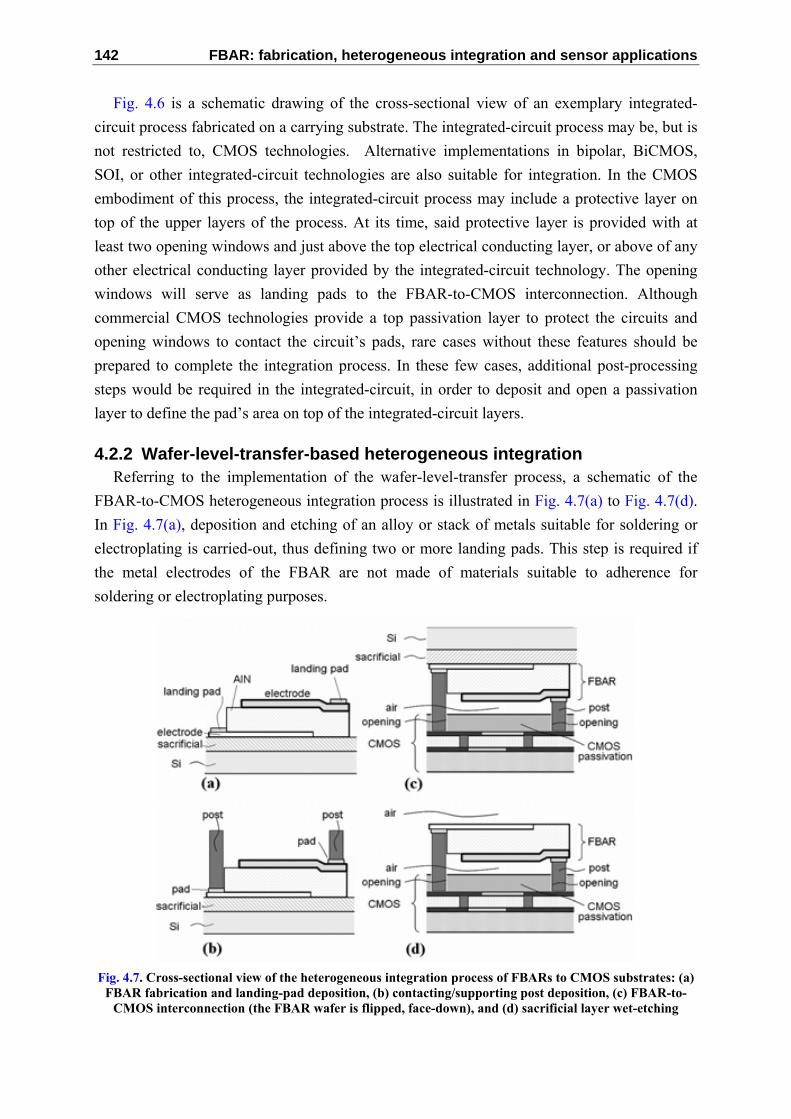
142 FBAR: fabrication, heterogeneous integration and sensor applications
Fig. 4.6 is a schematic drawing of the cross-sectional view of an exemplary integrated-circuit process fabricated on a carrying substrate. The integrated-circuit process may be, but is not restricted to, CMOS technologies. Alternative implementations in bipolar, BiCMOS, SOI, or other integrated-circuit technologies are also suitable for integration. In the CMOS embodiment of this process, the integrated-circuit process may include a protective layer on top of the upper layers of the process. At its time, said protective layer is provided with at least two opening windows and just above the top electrical conducting layer, or above of any other electrical conducting layer provided by the integrated-circuit technology. The opening windows will serve as landing pads to the FBAR-to-CMOS interconnection. Although commercial CMOS technologies provide a top passivation layer to protect the circuits and opening windows to contact the circuit’s pads, rare cases without these features should be prepared to complete the integration process. In these few cases, additional post-processing steps would be required in the integrated-circuit, in order to deposit and open a passivation layer to define the pad’s area on top of the integrated-circuit layers.
4.2.2 Wafer-level-transfer-based heterogeneous integration Referring to the implementation of the wafer-level-transfer process, a schematic of the
FBAR-to-CMOS heterogeneous integration process is illustrated in Fig. 4.7(a) to Fig. 4.7(d). In Fig. 4.7(a), deposition and etching of an alloy or stack of metals suitable for soldering or electroplating is carried-out, thus defining two or more landing pads. This step is required if the metal electrodes of the FBAR are not made of materials suitable to adherence for soldering or electroplating purposes.
Fig. 4.7. Cross-sectional view of the heterogeneous integration process of FBARs to CMOS substrates: (a)
FBAR fabrication and landing-pad deposition, (b) contacting/supporting post deposition, (c) FBAR-to-CMOS interconnection (the FBAR wafer is flipped, face-down), and (d) sacrificial layer wet-etching

Chapter 4. Heterogeneous integration of FBAR with CMOS technologies 143
In one embodiment of the technology, the materials composing the landing pads may be selected from the group of nickel, gold, titanium, among others. Fig. 4.7(b) illustrates how the connecting posts are placed on top of the landing pads. Connecting posts will provide support and electrical connection to the FBAR, giving the device its suspended configuration above described. The techniques and methods required to implement the posts are diverse and include mask-driven deposition of soldering paste, metal deposition, and electroplating assisted deposition, among others. Fig. 4.7(c) is a schematic describing the interconnection between the FBAR and CMOS substrates. First, the substrate carrying the FBAR is turned face-down, and aligned to the CMOS substrate. This is done to provide alignment between the connecting post and the opening window, and between the connecting post and the opening window. Manual or automatic pick-and-place systems may be used for positioning, alignment and soft-contacting of FBAR and CMOS wafers. Since the FBAR’s substrate is turned down during this step, the second electrode becomes now the closest one to CMOS substrate. At its time, the FBAR-carrying substrate is now the most top layer of the suspending structure. It is also to be noticed that, due to the bigger size of the connecting posts, compared to the FBAR’s thickness, an air interface is now created between the FBAR and the substrate. Mechanical interconnection of the connecting posts to the pads depends on the integration process. For example, the connecting posts may be soldering bumps that are heated and soldered to the integrated-circuit pads, in one side, and to the FBAR pads, in the other side. In other embodiments of this technology, soldering may be replaced by electroplating or deposition techniques, in order to achieve the interconnection depicted in Fig. 4.7(c).
In the last step of the process and referring to Fig. 4.7(d), final release of the FBAR is performed by wet etching of sacrificial layer, thus achieving complete integration between the FBAR and the substrate. Since the sacrificial layer is between the FBAR and the substrate, the latter is released when etching of the sacrificial layer is completed, thus separating the FBARs from the substrate. At this point the substrate is of no interest and is discarded for manufacturing purposes. At its time, the FBAR is fully released and connected to the CMOS substrate, which may be an only-supporting substrate, or may carry passive or active devices, or both. In the preferred application of this technique, the substrate carries integrated-circuit devices, thus providing fully-integrated FBAR-to-CMOS application system. It is to be noticed that after the releasing process of the sacrificial layer, the FBAR exhibits two air interfaces: one on top of the device, and the second one underneath the FBAR, respectively. Hence, the FBAR has mechanical freedom to vibrate since no acoustical coupling exists between it and any substrate. This feature is a necessary condition to guarantee good quality factors.
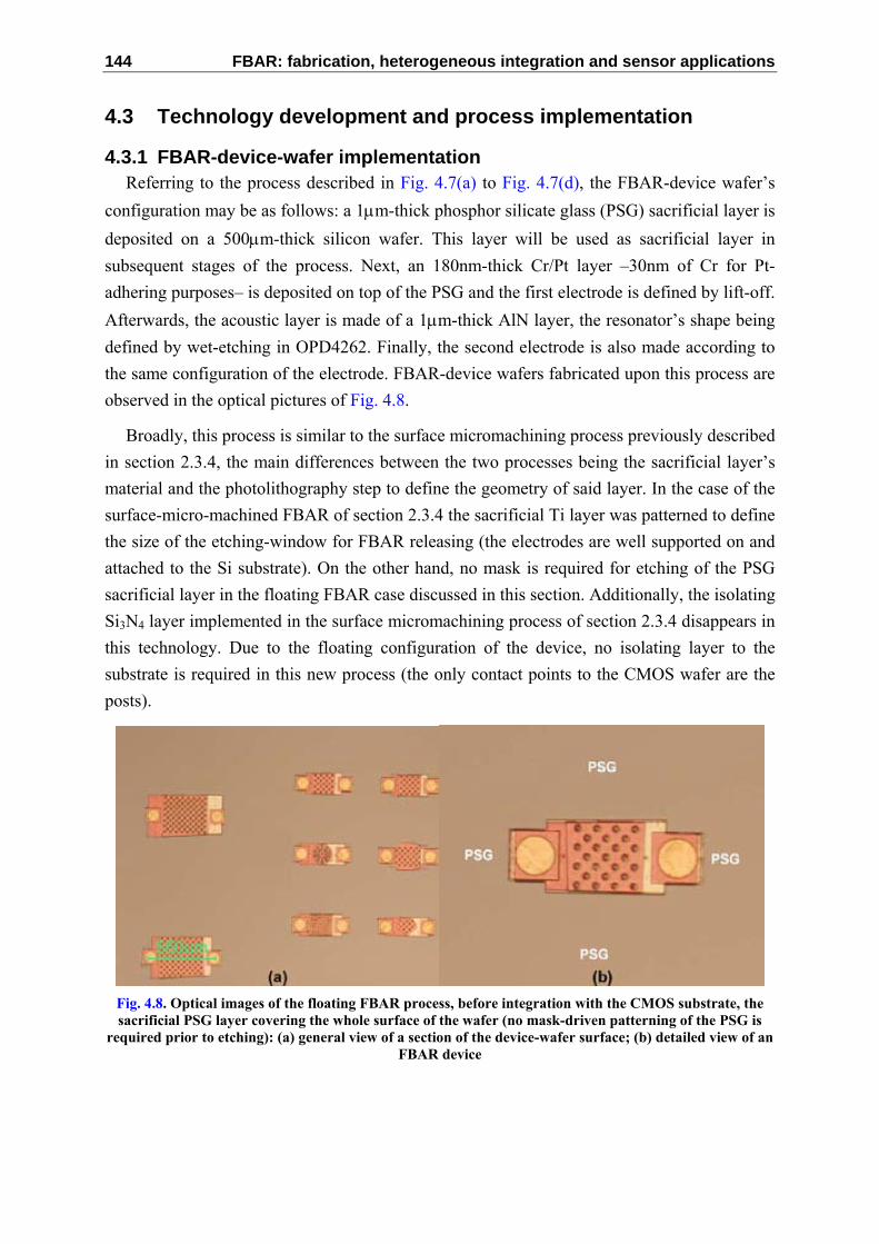
144 FBAR: fabrication, heterogeneous integration and sensor applications
4.3 Technology development and process implementation
4.3.1 FBAR-device-wafer implementation Referring to the process described in Fig. 4.7(a) to Fig. 4.7(d), the FBAR-device wafer’s
configuration may be as follows: a 1μm-thick phosphor silicate glass (PSG) sacrificial layer is deposited on a 500μm-thick silicon wafer. This layer will be used as sacrificial layer in subsequent stages of the process. Next, an 180nm-thick Cr/Pt layer –30nm of Cr for Pt-adhering purposes– is deposited on top of the PSG and the first electrode is defined by lift-off. Afterwards, the acoustic layer is made of a 1μm-thick AlN layer, the resonator’s shape being defined by wet-etching in OPD4262. Finally, the second electrode is also made according to the same configuration of the electrode. FBAR-device wafers fabricated upon this process are observed in the optical pictures of Fig. 4.8.
Broadly, this process is similar to the surface micromachining process previously described in section 2.3.4, the main differences between the two processes being the sacrificial layer’s material and the photolithography step to define the geometry of said layer. In the case of the surface-micro-machined FBAR of section 2.3.4 the sacrificial Ti layer was patterned to define the size of the etching-window for FBAR releasing (the electrodes are well supported on and attached to the Si substrate). On the other hand, no mask is required for etching of the PSG sacrificial layer in the floating FBAR case discussed in this section. Additionally, the isolating Si3N4 layer implemented in the surface micromachining process of section 2.3.4 disappears in this technology. Due to the floating configuration of the device, no isolating layer to the substrate is required in this new process (the only contact points to the CMOS wafer are the posts).
Fig. 4.8. Optical images of the floating FBAR process, before integration with the CMOS substrate, the sacrificial PSG layer covering the whole surface of the wafer (no mask-driven patterning of the PSG is
required prior to etching): (a) general view of a section of the device-wafer surface; (b) detailed view of an FBAR device

Chapter 4. Heterogeneous integration of FBAR with CMOS technologies 145
4.3.2 CMOS-substrate implementation As it was seen in Fig. 4.6, the CMOS substrate may be fabricated according to the typical
structure of a CMOS technology, thus implementing a top metal layer for interconnection purposes, which is covered by a dielectric passivation layer. This layer may be, for example, a 500nm-thick PECVD silicon oxide layer, with photolithography-defined openings for pad connection. The metal layer may be manufactured by implementing one or more of the following configurations: platinum over chromium, aluminum over chromium, aluminum over titanium (given appropriate burying of the Ti layer), among others. Depending on the available CMOS process, wet etching of the FBAR-CMOS ensemble may be performed using suitable etchant solutions. Or, in the case of technological options for the CMOS metallization, the CMOS metal-layer configuration may be selected to fit the etching requirements of the FBAR wafer. Two implementations of the heterogeneous-integration process were carried out in this work, using the in-house CNM25 CMOS and the Austria Micro Systems AMS035 technologies.
The first CMOS-substrate implementation was fabricated within the CNM25 process. According to the above-mentioned requirements, a set of technological options for the standard CMOS implementation was selected. In this process, an isolating Si3N4 layer was deposited on the surface of the Si substrate. Next, a Cr/Pt layer was deposited and patterned (lift-off) to define transmission lines and pad connections. In order to provide the process with adhesive metallization, a Ti/Ni/Au layer was deposited. After being deposited and patterned a passivation resist layer, two or more landing pads were available in the CMOS substrate for FBAR interconnection. In this process the resist accomplishes two purposes: it serves as mask for patterning of the Ti/Ni/Au, and at the same time it becomes the top’s passivation layer of the CMOS process. The surface of the CMOS-substrate wafer implemented with the CNM25 technology is observed in the optical micrograph of Fig. 4.9. A co-planar test structure was fabricated in order to perform electrical characterization of FBAR devices after the heterogeneous integration process. The space corresponding to the FBAR is still to be filled by the device when the pick and place processes are implemented.
Fig. 4.9. CNM25 2-metal technology implementation: (a) cross-sectional schematic view of the CNM25
process; (b) a co-planar test structure fabricated according to this process

146 FBAR: fabrication, heterogeneous integration and sensor applications
Fig. 4.10. AMS035 technology implementation of the CMOS-substrate for heterogeneous integration with
FBAR substrate: (a) cross-sectional schematic view of the AMS035 process; (b) optical image of a co-planar test structure implemented within this process (the FBAR is to be located in between the landing
pads)
A second implementation of the CNM-substrate was fabricated using one of the Austria Micro System’s (AMS) 0.35μm technologies (2-poly, 4-metal). Since the commercial AMS035 technology is a standard CMOS process, the design of a test structure followed the available layers and process parameters of this technology. In Fig. 4.10(a), a cross-sectional schematic drawing of the technology is depicted. It can be seen that a top passivation layer is available (PROT2). The top layer metallization (Metal 4) is implemented in Al/Ti, which is accessible by means of appropriate mask design and pad opening. In this way, the passivation layer on top of the FBAR’s landing pads is opened to leave the top metal layer (Metal 4) without the resist. Also for this technology, the same co-planar structures were designed, one sample being observed in the optical picture of Fig. 4.10(b). Again, the region between the landing pads will be occupied by the FBAR once the interconnection process of the FBAR and CMOS wafers is completed.
4.3.3. Compatibility testing In section 2.3.4 the compatibility testing of the surface micromachining technology was
described. In the same way, the compatibility of the FBAR-to-CMOS heterogeneous-integration process was tested. First, the metal electrode layers were analyzed. Since both the surface-micromachining and the heterogeneous integration technologies implement an adhesive metal layer (Cr) underneath the Pt metallization, the same testing results of section 2.3.4 were considered valid for the heterogeneous integration technology. However, some differences exist between these technologies, and new materials and processes had to be evaluated. For example, the sacrificial layer is now made of PSG, instead of Ti, as it was implemented in the surface micromachining process. Also, an additional Ti/Ni/Au layer is placed on top of the Cr/Pt metallization for the landing-pad implementation. For those reasons, the PSG etching rates and the selectivity of HF to Ti/Ni/Au had to be evaluated.
Given that the PSG is uniformly deposited on the whole surface of the FBAR-device wafer, the etching times were determined by the maximum-sized feature in the layout. In

Chapter 4. Heterogeneous integration of FBAR with CMOS technologies 147
order to reduce the etching times, a layout-design strategy consisting on through-holing of the devices was adopted. In this way, the FBAR’s layout is drilled, thus increasing the contact surface of the etching solution with the PSG underneath the FBAR (see Fig. 4.8). HF-etching of the PSG on the FBAR-device wafer revealed etching rates of around 120,000 Å/min, which are similar to those obtained for SiO2 in the surface micromachining process described in chapter 2. However, the etching time was reduced due to device-drilling (depending on the HF concentration and pitch of the holes, etching times between 1-5 min. were obtained).
The second test was focused on the HF-etching selectivity to the landing-pad and soldering-bump materials (Ti/Ni/Au and Sn/Pb, respectively). For that reason, test structures comprising Cr/Pt metallization, landing pads and soldering bumps were implemented. Among these structures, FBAR-device and CMOS wafers were fabricated, although testing FBAR-device wafers had not the PSG layer. In this experiment, we required a substrate with no PSG in order to observe the integrity of the pads and bumps without device de-attaching from the substrate. It is also to be noticed that the soldering bumps may be attached to the device or to the substrate wafer as well, although in the implemented wafers we placed the soldering bumps on the device’s wafer. Both samples –the test structure and the CMOS-substrate– were immersed in a buffered HF solution (49%). After few minutes (<5), the samples were taken out of the HF bath and cleansed in H2O2, with no damage of the pads and bumps, as it can be seen in the optical image of Fig. 4.11.
In summary, the heterogeneous integration technology proposed here is compatible with HF-based etching, with low complexity and reduced processing time. Now, the interconnection of the involved wafers and the release of the sacrificial layer can be completed, in order to achieve the FBAR-to-CMOS heterogeneous integration.
Fig. 4.11. Test structure for process compatibility evaluation: the chip in the image was immersed in HF
(49%), taken out after few minutes, and cleansed; with no significant damage in the soldering bumps observed
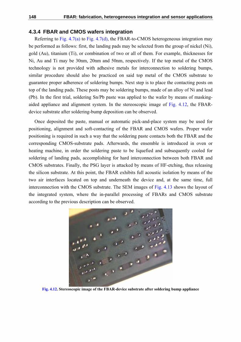
148 FBAR: fabrication, heterogeneous integration and sensor applications
4.3.4 FBAR and CMOS wafers integration Referring to Fig. 4.7(a) to Fig. 4.7(d), the FBAR-to-CMOS heterogeneous integration may
be performed as follows: first, the landing pads may be selected from the group of nickel (Ni), gold (Au), titanium (Ti), or combination of two or all of them. For example, thicknesses for Ni, Au and Ti may be 30nm, 20nm and 50nm, respectively. If the top metal of the CMOS technology is not provided with adhesive metals for interconnection to soldering bumps, similar procedure should also be practiced on said top metal of the CMOS substrate to guarantee proper adherence of soldering bumps. Next step is to place the contacting posts on top of the landing pads. These posts may be soldering bumps, made of an alloy of Ni and lead (Pb). In the first trial, soldering Sn/Pb paste was applied to the wafer by means of masking-aided appliance and alignment system. In the stereoscopic image of Fig. 4.12, the FBAR-device substrate after soldering-bump deposition can be observed.
Once deposited the paste, manual or automatic pick-and-place system may be used for positioning, alignment and soft-contacting of the FBAR and CMOS wafers. Proper wafer positioning is required in such a way that the soldering paste contacts both the FBAR and the corresponding CMOS-substrate pads. Afterwards, the ensemble is introduced in oven or heating machine, in order the soldering paste to be liquefied and subsequently cooled for soldering of landing pads, accomplishing for hard interconnection between both FBAR and CMOS substrates. Finally, the PSG layer is attacked by means of HF-etching, thus releasing the silicon substrate. At this point, the FBAR exhibits full acoustic isolation by means of the two air interfaces located on top and underneath the device and, at the same time, full interconnection with the CMOS substrate. The SEM images of Fig. 4.13 shows the layout of the integrated system, where the in-parallel processing of FBARs and CMOS substrate according to the previous description can be observed.
Fig. 4.12. Stereoscopic image of the FBAR-device substrate after soldering bump appliance
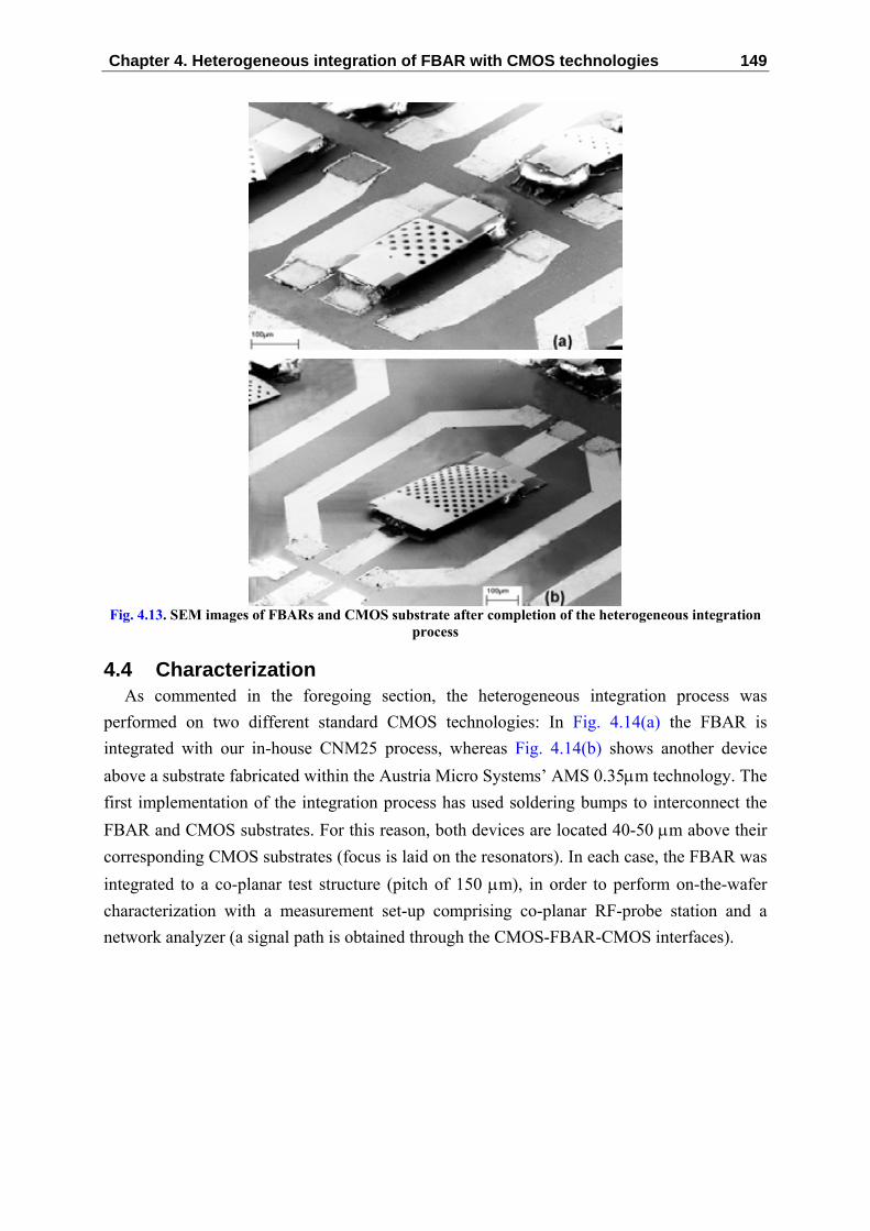
Chapter 4. Heterogeneous integration of FBAR with CMOS technologies 149
Fig. 4.13. SEM images of FBARs and CMOS substrate after completion of the heterogeneous integration
process
4.4 Characterization As commented in the foregoing section, the heterogeneous integration process was
performed on two different standard CMOS technologies: In Fig. 4.14(a) the FBAR is integrated with our in-house CNM25 process, whereas Fig. 4.14(b) shows another device above a substrate fabricated within the Austria Micro Systems’ AMS 0.35μm technology. The first implementation of the integration process has used soldering bumps to interconnect the FBAR and CMOS substrates. For this reason, both devices are located 40-50 μm above their corresponding CMOS substrates (focus is laid on the resonators). In each case, the FBAR was integrated to a co-planar test structure (pitch of 150 μm), in order to perform on-the-wafer characterization with a measurement set-up comprising co-planar RF-probe station and a network analyzer (a signal path is obtained through the CMOS-FBAR-CMOS interfaces).

150 FBAR: fabrication, heterogeneous integration and sensor applications
Fig. 4.14. Top-view optical images of floating FBAR integrated with two different CMOS substrates: (a)
in-house standard CMOS, and (b) AMS 0.35 μm technology
In Fig. 4.15 the magnitude and phase of the S21 parameter of an exemplary device are plotted, a resonance frequency of around 2.4 GHz being observed. Looking at these curves, it should be said that larger variations in both the attenuation and phase shift are required to accomplish the in-band and out-of-band specifications of modern filter-applications. This goal can be achieved with higher quality factor (Q) devices by means of appropriate layout design of the electrodes, among other actions [23]. Due to the direct relationship between the Q factor and the FBAR’s electrode area, bigger devices will exhibit higher Q-factors. This observation links to the Q-factor analysis presented in the next paragraph.
The Q factor of floating and conventional FBAR devices is compared in Fig. 4.16 (conventional FBARs were designed with the same layout and released by means of front-side reactive-ion-etching (RIE) of silicon, see inset in the figure). As observed, the floating FBAR process exhibits similar performance, or better, than the RIE-based process (lower substrate losses).
Fig. 4.15. Electrical characterization of FBAR integrated with CNM25 standard-CMOS substrate:
Magnitude and phase of the transmission (S21) parameter (characterized device in the SEM image of the inset)

Chapter 4. Heterogeneous integration of FBAR with CMOS technologies 151
Fig. 4.16. Quality factor performance of the floating FBAR compared to similar devices fabricated with
reactive-ion-etching (RIE) technology (exemplary devices of each technology in the insets)
However, the Q factor is still low for accomplishing the stringent requirements of modern integrated-system applications. This may be explained by the through-holed layout design of the FBARs: the Q factor of longitudinal-mode devices is reduced when milling or drilling is practiced on the device’s structure. This is due to mode-shape modification, increased energy dissipation at resonance and effective-area decrease [23] (we verified a Q factor higher than 700 for non-drilled RIE-based devices of the same geometry, which is one order of magnitude better than for drilled FBAR).
At the current state of this work, only through-hole floating FBARs have been implemented, although devices with no holes will be designed in the future (high sacrificial-layer etching-rates and the low impact of aggressive etchants in the FBAR’s structure have demonstrated that this is feasible with no significant process trade-off). Electroplating-based deposition of the contacting-posts will improve the overall cleanness and performance of the process so far.
4.5 Technology optimization In sections 4.2 and 4.3 the technology required for landing pad and supporting posts
fabrication was described. In its current state, a Sn/Pb alloy paste deposited on either the device or CMOS wafers performs the interconnection of the ensemble. Due to its composition and physical consistency, implementation of this alloy makes the efficiency and cleanness of the process to be very low. First, the pitch between the soldering bumps has to be at lest 250μm, each bump having a diameter of 80μm (after heating). This leads to bigger-device layout design, thus increasing the die area. As a consequence, the mechanical rigidity and stability of the devices is reduced. A third drawback of this method is that post-integration cleaning of the integrated wafers is required, due to residual composites deposited on the surface of the CMOS wafer (and/or the FBAR wafer), as co-lateral products of bump melting.

152 FBAR: fabrication, heterogeneous integration and sensor applications
Additionally, the electrical properties of the soldering bumps as interconnecting paths are still to be studied, especially for the GHz-range frequency band.
Another technological possibility to supporting-post fabrication is electroplating. With this option, the soldering paste is replaced by the more-uniform electroplated column, grown on top of either the CMOS or the FBAR wafers. The resulting product is a cleaner and sharper FBAR-CMOS ensemble, with reduced pitch dimensions and, consequently, with improved area-efficiency. No additional layout-design effort is required, since the same mask for landing-pad and soldering-bump definition is re-used for the electroplated post. The technological process of the optimized FBAR-CMOS integration is described in the sequence of Fig. 4.17. Beginning from the FBAR fabrication, the first electrode, the AlN layer, and the second electrode are successively deposited on top of a sacrificial layer, which can also be PSG, as depicted in Fig. 4.17(a). Next, a passivation layer is deposited and patterned using the same mask of the process described in sections 4.2 and 4.3 for landing-pad deposition (Fig. 4.17(b)). Typically, this layer is a thick resist and will be used to define the electroplating area. The next step is the deposition of the seed material for electroplating, which can be a Ti/Ni layer (Fig. 4.17(c)). Since the process is intended for wafer-level integration, the seed material is deposited along the whole wafer’s surface.
Fig. 4.17. Optimized process sequence for heterogeneous integration of FBAR and CMOS wafers: (a) FBAR fabrication; (b) resist deposition; (c) seed material; (d) oxide deposition; (e) electroplating; (f)
resist-oxide removing; (g) FBAR-CMOS wafers integration; (h) sacrificial layer etching (FBAR released)

Chapter 4. Heterogeneous integration of FBAR with CMOS technologies 153
Next, the same mask of step (b) is again implemented to pattern another passivation layer, as depicted in Fig. 4.17(d). This second passivation layer will contribute to limit the growing area of the electroplated material, according to the supporting post mask design (Fig. 4.17(e)).
Once finished the electroplating deposition, the resist, seed material and second passivation layers are removed to provide the final shape of the FBAR wafer before the integration (Fig. 4.17(f)). It is to be noted that the steps (b) to (f) could also be performed on the CMOS wafer. However, in spite of the standard nature of the CMOS process, we prefer the above-described implementation, which describes a more general solution. The last two steps are basically the same already described in section 4.2, where the FBAR-CMOS interconnection is carried out (Fig. 4.17(g)) and the sacrificial layer attacked to release the Si substrate, thus completing the process (Fig. 4.17(h)).
A mask set regarding this process was designed and the FBARs are currently being fabricated within the CNM25 process. The new design has allowed reductions of the supporting posts diameter and pitch: in the previous implementation the diameter and minimum pitch were of 80μm and 250μm, respectively. With the optimization introduced by this process, the new diameter and pitch values are of 25μm and 100μm, respectively. Shrinking the posts dimensions and pitch is of special relevance on this integration approach, because it permits a more compact and robust design of the FBAR’s structure. Since the effective resonator area is defined by the AlN and electrodes intersection, the remaining electrode’s and AlN area can be reduced to provide shorter structures, which can alleviate the high stress of the floating FBAR’s structure. Additionally, this feature lets a higher FBAR density in the wafer, due to reduced distance between them. These effects are illustrated by the schematic drawings of Fig. 4.18. Top-view representations of FBARs and their corresponding pads, showing the pad-size reduction effect of the optimized electroplating process, are shown in Fig. 4.18(a). In the same way, the pitch reduction permits a higher number of FBARs to be located on a determined area, as depicted in Fig. 4.18(b). Clearly, the new structures are expected to be more robust and more efficient.
Fig. 4.18. FBAR’s layout optimization due to the electroplating-based fabrication of the supporting posts:
(a) Pitch reduction; (b) Pad-size reduction, compared in both cases to the soldering bump process

154 FBAR: fabrication, heterogeneous integration and sensor applications
4.6 Summary A method for performing heterogeneous integration of FBAR with CMOS technologies
was presented [24]. The heterogeneous integration of FBAR and CMOS substrates has been accomplished, the FBAR exhibiting a floating, three-dimensional structure above the CMOS [25]. The fabrication technology provides with compatibility for both the FBAR and the CMOS processes, in order to integrate them into compact RF or sensor applications. Since the processes do not require special manufacturing restrictions –like deposition temperature of the acoustic layer–, enhanced flexibility and versatility may be achieved for the FBAR-to-CMOS interconnection technology. Future interconnection of the floating-FBAR structure to CMOS substrates carrying integrated-circuitry will demonstrate all the potential of the heterogeneous-integration technology introduced in this work.
This technology has many benefits to other FBAR-CMOS integration approaches (or to other suitable MEMS-to-CMOS integration technologies). Compared to the standard flip-chip implementation [1], for example, our method presents two main advantages: wafer-level integration and no FBAR-carrying substrate attached to the resonator. This approach saves the long processing time of batch FBAR-to-CMOS integration. Another difference is that the packaging approach of our work is not only a protective means [4], but also an interconnection element in the integration ensemble. On the other hand, we take advantage of all the benefits and flexibility of heterogeneous integration, avoiding the constraints of costly and technology-specific monolithic integration [3]. In summary, some of the main benefits introduced by the heterogeneous integration approach presented here can be stated as:
• Fabrication of the FBAR and its integration with CMOS integrated circuit in the same step of the manufacturing process.
• Technology-independent FBAR-to-CMOS integration process.
• No need of integration-oriented technology development for the FBAR technology (FBAR may be fabricated even within high-temperature processes).
• No need of integration-oriented technology development for the IC technology.
• Versatility and flexibility of the IC technology to be integrated with the FBAR.
• Reduced number of steps of the FBAR’s fabrication process.
• Versatility and flexibility of integration level, being possible to perform wafer-level or die-level integration.
• Reduced die area (compared to FBAR-to-CMOS hybrid integration and to FBAR-on-side-of-IC, as well).
• Versatility and flexibility of the technology providing electrical interconnection between FBAR and IC (compared to hybrid or monolithic integration).

Chapter 4. Heterogeneous integration of FBAR with CMOS technologies 155
Nevertheless, the development of a competitive FBAR-CMOS integrated system confronts many challenges. First, the interconnection technology has to be optimized, in order to reduce the landing pad and soldering bump sizes. By reducing the size of the landing pads, the die density can be improved (the transmission lines occupy significant die area). At the same time, a cleaner interconnection technology will help to reduce insertion losses and cleaning time (during fabrication). Electroplating technology is a suitable alternative for achieving of this purpose. On the other hand, the thin-film stress becomes more critical, since no clamping points others than the posts are available on the floating FBAR devices. This entails new design efforts on the future optimization of the FBAR’s layout.
References 1 B. P. Otis, and J. M. Rabaey, “A 300-μW 1.9-GHz CMOS oscillator utilizing micromachined
Resonators”, IEEE J. Solid-State Circuits 38 (2003) 1271-1274. 2 F. Vanhelmont, P. Philippe, A.B.M. Jansman, R.F. Milsom, J.J.M. Ruigrok, and A. Oruk, “A
2GHz reference oscillator incorporating a temperature compensated BAW resonator”, in Proc. IEEE Intl. Ultrason. Symp. 2006, Oct. 3-6 2006, Vancouver, Canada, 333-336.
3 M.-A. Dubois, C. Billard, C. Muller, G. Parat, and P. Vincent, “Integration of high-Q BAW resonators and filters above IC”, in IEEE Intl. Solid-State Circuits Conf. Dig. of Tech. Papers, 2005, Feb. 6-10 2005, San Francisco CA, USA, 392-393.
4 D. Feld, P.Bradley, A. Barfknecht, and R. Ruby, “A wafer level encapsulated FBAR chip molded into a 2.0 mm /spl times/ 1.6 mm plastic package for use as a PCS full band Tx filter”, in Proc. IEEE Intl. Ultrason. Symp. 2003, Oct. 5-8 2003, Honolulu Hawaii, USA, 2, 1798-1801.
5 J.A. Chediak, Z. Luo, J. Seo, N. Cheung, L.P. Lee, and T.D. Sands, “Hybrid integration of CdS filters with GaN LEDs for biophotonic chips”, in Proc. IEEE Intl. Conf. on MEMS 2003, 19-23 Jan., 2003, Tokyo, Japan, 323- 326.
6 W.C. Dunn, H.M. Liaw, L. Ristic, and R.M. Roop, “Monolithic circuit with integrated bulk structure resonator”, U.S. patent no. 5,260,596, Nov. 1993.
7 K. Lee, Y. S. Eo, and S. Hyun, “Single-chip radio structure with piezoelectric crystal device integrated on monolithic integrated circuit and method of fabricating the same”, U.S. patent no. 6,285,866, Sep. 2001.
8 D. Figueredo, R. C. Ruby, Y. Oshmyansky, and P. Bradley, “Thin film bulk acoustic resonator (FBAR) and inductor on a monolithic substrate and method of fabricating the same”, U.S. patent no. 6,710,681, Mar. 2004.
9 M. Furuhata, A. Yajima, K. Goto, H. Sato, T. Funasaka, S. Kawano, S. Fujii, T. Higuchi, M. Ueno, “Development of Monolithic CMOS-SAW Oscillator”, in Proc. IEEE Intl. Ultrason. Symp., 2005, Sept. 18-21, 2005, Rotterdam, The Netherlands, 4, 2194-2197.
10 J. Verd, A. Uranga, J. Teva, J. L. López, F. Torres, J. Esteve, G. Abadal, F. Pérez-Murano, and N. Barniol, “Integrated CMOS–MEMS with on-Chip readout electronics for high-frequency applications”, IEEE Electron Dev. Lett. 27 (2006), 495-497.
11 B. Ilic, H. G. Craighead, S. Krylov, W. Senaratne, C. Ober, and P. Neuzil, “Attogram detection using nanoelectromechanical oscillators”, J. Appl. Phys. 95 (2004) 3694-3703.
12 J. Geske, Y.L. Okuno, J.E. Bowers, and V. Jayaraman, “Vertical and lateral heterogeneous integration”, Appl. Phys. Lett. 79 (2001) 1760-1762.
13 F. Roozeboom, A.L.A.M. Kemmeren, J.F.C. Verhoeven, F.C. van den Heuvel, J. Klootwijk, H. Kretschman, T. Frič, E.C.E. van Grunsven, S. Bardy, C. Bunel, D. Chevrie, F. LeCornec, S. Ledain, F. Murray and P. Philippe, “Passive and heterogeneous integration towards a Si-based System-in-Package concept”, Thin Solid Films 504 (2006), 391-396.
14 IBM Zurich Research Laboratory, “Device integration”, Available on-line (accessed November 2007): http://www.zurich.ibm.com/st/server/microdevice.html
15 T. Shimoda and S. lnoue, “Surface free technology by laser annealing (SUFTLA)”, in IEEE Electron Devices Meeting IEDM 1999 Digest Tech. Papers, 5-8 Dec. 1999, Washigton, DC, USA,

156 FBAR: fabrication, heterogeneous integration and sensor applications
pp. 289-292. 16 S. Inoue, S. Utsunomiya, T. Saeki, and T. Shimoda, “Surface-free technology by laser annealing
(SUFTLA) and its application to poly-Si TFT-LCDs on plastic film with integrated drivers”, IEEE T. Electron Devices 49 (2002) 1353-1360.
17 M. B. Cohn, and J.-H. Xu, “MEMS device with integral packaging”, U.S. patent no. 6,872,902 B2, Mar. 2005.
18 P. Bradley, J. D. Larson III, and R. C. Ruby, “Mounting film bulk acoustic resonators in microwave packages using flip-chip bonding technology”, U.S. patent no. 6,550,664 B2, Abr. 2003.
19 P. Bradley, “Packaging methodology for duplexers using FBARs”, U.S. patent no. 6,838,956 B2, Jan. 2005.
20 J. A. Philliber, and R. C. Ruby, “Method of fabricating a semiconductor device and an apparatus embodying the method”, U.S. patent no. 6,794,958 B2, Sep. 2004.
21 E. Bar-Sadeh, A. Talalyevsky, and E. Ginsburg, “Reduced substrate micro-electro-mechanical systems (MEMS) device and system for producing the same”, U.S. patent no. 6,894,383 B2, May. 2005.
22 [27] E.-K. Kim, “Thin film resonator and method for manufacturing the same”, U.S. patent no. 6,849,475 B2, Feb. 2005.
23 Q.X. Su, P. Kirby, E. Komuro, M. Imura, Q. Zhang, R. Whatmore, “Thin-film bulk acoustic resonators and filters using ZnO and leadzirconium-titanate thin films”, IEEE T. Microwave Theory Tech. 49 (2001) 769-778.
24 H. Campanella, J. Esteve, E. Cabruja, J. Montserrat, L. Terés, M. Carmona, “Thin-film bulk acoustic wave resonator and method for performing heterogeneous integration of the same with complementary-metal-oxide-semiconductor integrated circuit”, European Patent Office App. no. 07380041.9, Feb. 2007.
25 H. Campanella, E. Cabruja, J. Montserrat, A. Uranga, N. Barniol, and J. Esteve, “Thin-film bulk acoustic wave resonator floating above CMOS substrate”, IEEE Electron Device Lett. 29 (2008) 28-30.

CHAPTER 5
FBAR-based sensor applications
FBAR devices find application in a variety of systems, ranging from radio-frequency (RF) to
sensing components. Although the telecommunication industry has been the very first engine stimulating the development of FBARs, new sensing applications have been demonstrated in the past few years.
In FBAR-based sensor applications, one or more FBAR devices are composing elements of a system operating under piezoelectric actuation or detection mechanisms. Mass sensors, biochemical, liquid or gas detectors, are some examples. All these applications work under the same principle of quartz crystal microbalances (QCM), which is mass loading of the resonator’s structure. According to this principle, mass deposition on one of the FBAR electrodes gives rise to down-shifting of the resonance frequency. On the other hand, FBARs have the potential for implementation as mechanical sensors, like accelerometers or AFM-probe detectors.
In this chapter new applications of FBARs are introduced. In section 5.1 we report a novel, localized-mass sensor. Experimental and modeling results are presented and the benefits and challenges of the sensor’s technology discussed. In section 5.2 the fabrication technology and characterization results of FBAR-based mechanical sensors are presented. Next in section 5.3, the concept and first characterization results of a new contact-free acoustic resonator are discussed
5.1 Mass sensors FBARs exhibit high frequency and mass sensitivities, thus making this technology a
suitable candidate for bio-molecular or chemical-detection applications. Mass-sensing systems, in which quartz microbalances (QCM) have been the key technology, are now re-thought to be implemented with FBARs, taking advantage of its higher sensitivity compared to conventional QCMs [1-4]. Other technological approaches like nano-electro-mechanical (NEMS) resonators have also proved to achieve a very high sensitivity in localized-mass detection applications [5-7]. In this chapter we present two implementations of FBAR-based mass sensors, the first one being a distributed-mass sensor and the second one a localized-mass sensor. Sensing performance and application perspectives are discussed, for the study of sensitivity and possible configurations in biological applications. Different aspects of the
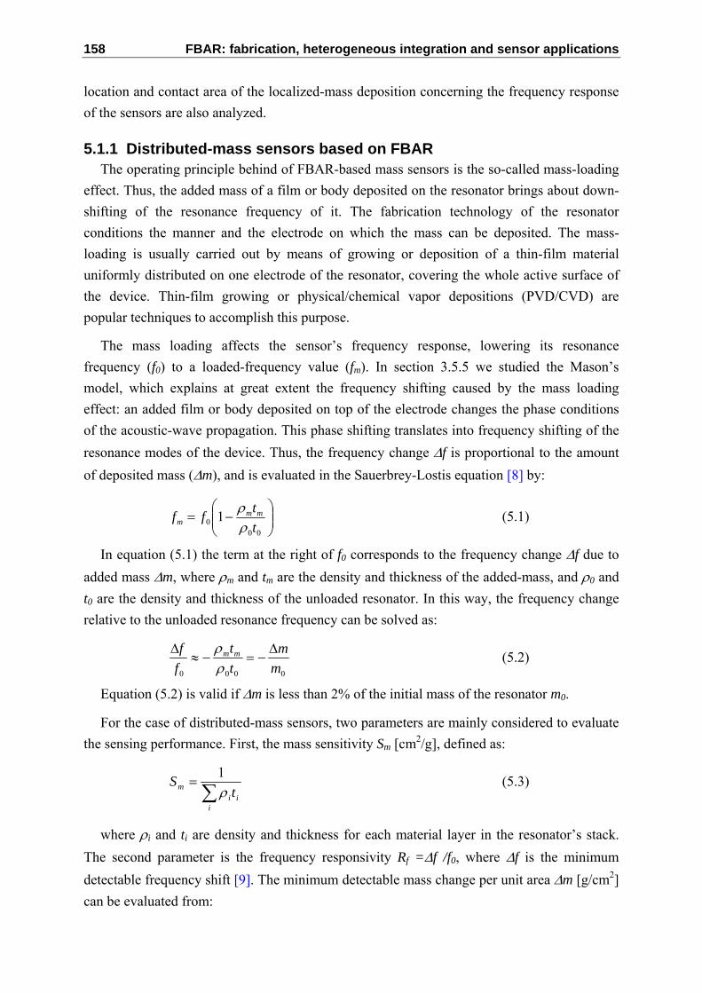
158 FBAR: fabrication, heterogeneous integration and sensor applications
location and contact area of the localized-mass deposition concerning the frequency response of the sensors are also analyzed.
5.1.1 Distributed-mass sensors based on FBAR The operating principle behind of FBAR-based mass sensors is the so-called mass-loading
effect. Thus, the added mass of a film or body deposited on the resonator brings about down-shifting of the resonance frequency of it. The fabrication technology of the resonator conditions the manner and the electrode on which the mass can be deposited. The mass-loading is usually carried out by means of growing or deposition of a thin-film material uniformly distributed on one electrode of the resonator, covering the whole active surface of the device. Thin-film growing or physical/chemical vapor depositions (PVD/CVD) are popular techniques to accomplish this purpose.
The mass loading affects the sensor’s frequency response, lowering its resonance frequency (f0) to a loaded-frequency value (fm). In section 3.5.5 we studied the Mason’s model, which explains at great extent the frequency shifting caused by the mass loading effect: an added film or body deposited on top of the electrode changes the phase conditions of the acoustic-wave propagation. This phase shifting translates into frequency shifting of the resonance modes of the device. Thus, the frequency change Δf is proportional to the amount of deposited mass (Δm), and is evaluated in the Sauerbrey-Lostis equation [8] by:
⎟⎟⎠
⎞⎜⎜⎝
⎛−=
000 1
ttff mm
m ρρ (5.1)
In equation (5.1) the term at the right of f0 corresponds to the frequency change Δf due to added mass Δm, where ρm and tm are the density and thickness of the added-mass, and ρ0 and t0 are the density and thickness of the unloaded resonator. In this way, the frequency change relative to the unloaded resonance frequency can be solved as:
0000 mm
tt
ff mm Δ
−=−≈Δ
ρρ (5.2)
Equation (5.2) is valid if Δm is less than 2% of the initial mass of the resonator m0.
For the case of distributed-mass sensors, two parameters are mainly considered to evaluate the sensing performance. First, the mass sensitivity Sm [cm2/g], defined as:
∑=
iii
m tS
ρ1 (5.3)
where ρi and ti are density and thickness for each material layer in the resonator’s stack. The second parameter is the frequency responsivity Rf =Δf /f0, where Δf is the minimum detectable frequency shift [9]. The minimum detectable mass change per unit area Δm [g/cm2] can be evaluated from:

Chapter 5. FBAR-based sensor applications 159
m
f
SR
m =Δ (5.4)
In the same way, the mass responsivity per area rm [g/Hz/cm2] is calculated from:
mm Sf
r×
=0
1 (5.5)
Although it is more applied to localized-mass detectors, another useful definition is the mass responsivity Rm [Hz/g], which is the change in frequency response per unit mass change. In certain cases, however, it is more convenient to deal with the inverse responsivity Rm
-1 [g/Hz]. Also, in this work the word responsivity will be used to express inverse responsivity, the minimum detectable mass change being calculated as the product Δf×Rm [10]. A typical value of rm for a QCM operating at 40 MHz can be found in the units of ng/Hz/cm2, whilst for an FBAR operating at 1 GHz this value reaches the units of pg/Hz/cm2, i.e. 1,000 better for the latter. Due to the smaller size of an FBAR, and the higher acoustic constants and densities of the materials used in its fabrication –usually AlN or ZnO–, its mass sensitivity is quite higher than for QCMs [11-13].
As already discussed in chapter 3, a thin-film of magnesium fluoride (MgF2) was deposited on the whole surface of rectangular FBARs –50×70μm2– for tuning of the resonance frequency, by means of physical-vapor-deposition (PVD). Thin-film thicknesses of 2, 5, 10 and 20nm were analyzed, and a responsivity Rm value of 1.4×10⁻¹⁷ g/Hz was calculated. It was also commented that these depositions did not exceed the limits for the Sauerbrey-Lostis equation to be valid, the ratio Δm/m0 being between 0.06 and 0.64%. A linear responsivity behavior was observed for thin-film deposition (Fig. 5.1). Now and based on those experiments, we study the performance of the thin-film-deposited FBAR as a distributed-mass sensor.
Fig. 5.1. Frequency shift of the resonance frequency against the amount of uniform-film-deposited mass on top of the FBAR

160 FBAR: fabrication, heterogeneous integration and sensor applications
First, the theoretical and experimental values of the mass responsivity per area rm are calculated. From the frequency shifting and deposited-mass data shown in Fig. 5.1, the theoretical value of the mass sensitivity Sm is calculated from equation (5.3) by taking into account each layer in the FBAR’s stack configuration. Once obtained Sm, the responsivity rm value is obtained by means of the inverse product of Sm by the series resonance frequency (2.4GHz), as expressed in equation (5.5). Table 5.1 shows the sensitivity and responsivity values for each layer composing the FBAR-sensor configuration and for the overall device as well. A thin-film of 20nm of MgF2 is used to calculate these parameters.
Now, we are interested on find the experimental sensitivity of the FBAR-based sensor. For this purpose, the minimum mass change Δm and the minimum detectable frequency Δf are to be evaluated. The experimental, minimum mass change Δm that can be detected with the current measurement set-up and FBAR configuration is evaluated by checking the minimum detectable frequency shift Δf, which can be found from the phase of the S21 parameter. First, the phase noise Δφ is quantified from a zero-span acquisition at the series resonance frequency f0. Thus, Δf may be found by dividing Δφ by the S21 phase-slope φm, evaluated at the resonance frequency f0:
0fm
fφ
φΔ=Δ (5.6)
Table 5.1. Theoretical mass sensitivity and responsivity of the FBAR-based uniform-mass sensor
FBAR’s layer Density ρi [g/cm3]
Thickness ti [cm]
Layer sensitivity Si=1/( ρi ti)
Inverse layer sensitivity
mi=Si-1
MgF2 3.176 2.0×10⁻⁶ 157,430.73 6.35×10⁻⁶
Pt (top) 21.45 1.5×10⁻⁵ 3,108.00 3.22×10⁻⁴
Ti (top) 4.506 3.0×10⁻⁶ 73,975.44 1.35×10⁻⁵
AlN 3.260 1.0×10⁻⁴ 3,067.48 3.26×10⁻⁴
Pt (bottom) 21.45 1.5×10⁻⁵ 3,108.00 3.22×10⁻⁴
Ti (top) 3.176 3.0×10⁻⁶ 73,975.44 1.35×10⁻⁵
Distributed-mass sensitivity Sm
[cm2/g] ∑
==
iii
m tmS
ρ1
0
997.12
Mass-responsivity per area rm [g/Hz/cm2] m
m Sfr
×=
0
1 4.18×10⁻¹³
In Fig. 5.2, an exemplary zero-span acquisition of the S21 phase is plotted. As observed, the maximum phase deviation from the mean value is ±0.08 deg, which is divided by the
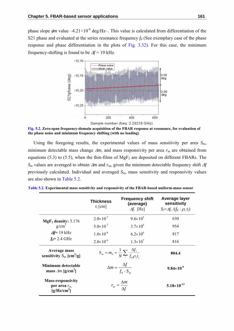
Chapter 5. FBAR-based sensor applications 161
phase slope φm value –4.21×10⁻⁶ deg/Hz–. This value is calculated from differentiation of the S21 phase and evaluated at the series resonance frequency f0 (See exemplary case of the phase response and phase differentiation in the plots of Fig. 3.32). For this case, the minimum frequency-shifting is found to be Δf = 19 kHz.
Fig. 5.2. Zero-span frequency-domain acquisition of the FBAR response at resonance, for evaluation of the phase noise and minimum frequency shifting (with no loading)
Using the foregoing results, the experimental values of mass sensitivity per area Sm, minimum detectable mass change Δm, and mass responsivity per area rm are obtained from equations (5.3) to (5.5), when the thin-films of MgF2 are deposited on different FBARs. The Sm values are averaged to obtain Δm and rm, given the minimum detectable frequency shift Δf previously calculated. Individual and averaged Sm, mass sensitivity and responsivity values are also shown in Table 5.2.
Table 5.2. Experimental mass sensitivity and responsivity of the FBAR-based uniform-mass sensor
Thickness ti [cm]
Frequency shift (average)
Δfi [Hz]
Average layer sensitivity
Si=Δfi /(f0 ⋅ ρi ti)
2.0×10⁻⁷ 9.6×10⁵ 630
5.0×10⁻⁷ 3.7×10⁶ 954
1.0×10⁻⁶ 6.2×10⁶ 817
MgF2 density: 3.176 g/cm3
Δf= 19 kHz f0= 2.4 GHz
2.0×10⁻⁶ 1.3×10⁷ 816
Average mass sensitivity Sm [cm2/g] ∑ Δ
==i ii
im tf
fN
mSρ0
01 804.4
Minimum detectable mass Δm [g/cm2] mSf
fm⋅
Δ=Δ
0
9.84×10⁻⁹
Mass-responsivity per area rm [g/Hz/cm2] f
mrm ΔΔ
= 5.18×10⁻¹³

162 FBAR: fabrication, heterogeneous integration and sensor applications
According to Table 5.1 and Table 5.2, the FBAR exhibits experimental uniform-film mass sensitivity and responsivity values over 80% of the theoretical values, for its Pt/Ti/AlN/Pt/Ti stack configuration. On the other hand, the experimental, minimum mass change Δm of 9.8ng/cm2 that can be detected with the current measurement set-up and FBAR configuration is pretty competitive to similar mass-sensing technologies. In Table 5.3 four different realizations are compared, including a quartz-based QCM sensor. As it can be seen, the overall performance of our uniform-film mass-sensor is similar to other implementations. Its highest resonance frequency is the main reason for such a remarkable performance, and the technological advantage of FBAR-based mass sensors.
After preliminary exploration of the uniform-mass sensing capabilities of our FBARs, the localized-mass sensing possibilities of the FBAR were explored. In the following sections, different localized-mass sensor experiments are described. These experiments were conducted with the aim of determining the sensitivity and responsivity of the sensor upon different sensing configurations.
5.1.2 The localized-mass sensor For the purpose of concept demonstration, focused-ion-beam-assisted deposition of a
localized-mass on the top electrode of the FBAR was carried out, according to the procedures previously presented in Chapter 3. The term "localized-mass" is defined as a material or compound deposited on the electrode of the FBAR, its dimensions being small enough compared to the electrode's area. The SEM image of Fig. 5.3 shows an example of this concept, a C/Pt/Ga deposited by FIB on the top electrode of an FBAR being observed [1].
Table 5.3. Uniform-mass-sensing performance for different FBAR realizations (longitudinal-resonance mode)
This work QCM (10 MHz)
Weber et al. 2006 [13]
FBAR (1.5 GHz) Zhang et al.
2005 [4]
FBAR (2GHz) Weber et al.
2006 [13] Minimum detectable
frequency shift Δf [Hz]
19,000 1 400 15,400
Average mass sensitivity Sm
[cm2/g] 804.4 0.54 726 937.5
Minimum detectable mass
Δm [g/cm2] 9.8×10⁻⁹ 5.2×10⁻⁹ 1.0×10⁻⁹ 21×10-9
Mass-responsivity per area rm [g/Hz/cm2]
5.18×10⁻¹³ 1.79×10⁻¹² 9.18×10⁻¹³ 1.36×10⁻¹²

Chapter 5. FBAR-based sensor applications 163
Fig. 5.3. Localized-mass deposited on the top electrode of an FBAR (after [1]: Campanella et al., 2006)
The size and location of the mass have been proven to affect the localized-mass sensor’s performance, as we have demonstrated [14, 15]. These aspects and the different sensor configurations are further discussed in the following sections. As commented previously, the performance of a localized mass deposition is well evaluated by means of the mass responsivity Rm [Hz/g], which is the change in frequency response per unit mass change. Also, it was said that, in certain cases, it is more convenient to deal with the inverse responsivity Rm
-1[g/Hz]. Along this chapter, the word responsivity will be used to express inverse responsivity, the minimum detectable mass change being calculated as the product Δf×Rm [10]. We will use these metrics to evaluate our localized-mass sensor’s performance. This section is thus focused on explaining the experiments and the impact of both aspects on the mass-sensing performance based on FBAR, with the aim of future-application development.
A first localized-mass deposition experiment, intended for the study of the mass dependency of responsivity, was carried out by depositing a 1.5×1.5 μm2 square-shaped composite of C/Pt/Ga on the geometric center of the top electrode of a group of resonators. A localized-mass of different thickness was deposited on each FBAR, in order to explore a range of masses. In this experiment we tested thicknesses of 1, 20, 100 and 400 nm, corresponding to a range of deposited masses between 9.0×10⁻¹⁵ g and 3.6×10⁻¹² g. In Fig. 5.4 the change of resonance frequency against the amount of deposited mass is plotted. Due to the wide range of deposited mass, the x-axis is presented in logarithmic scale.
In this figure, we can analyze responsivity [g/Hz]. In this experiment, the mass responsivity of the studied FBARs changes from tens of zg/Hz to ag/Hz. This value is competitive with respect to other NEMS technologies previously reported [5-7], and is specific for this mass-loading configuration. Later in this section, it will be shown that responsivity depends on both location and area of the localized-mass.

164 FBAR: fabrication, heterogeneous integration and sensor applications
Fig. 5.4. Frequency shifting against mass-loading: different masses with the same contact-area -1.5×1.5
μm2- are deposited on the center of the top electrode of the FBAR sensors
As commented previously, the mass-sensitivity [g] –minimum mass change that can be detected with the current measurement set-up and FBAR configuration– can be predicted by measuring the minimum frequency-shifting Δf that the set-up is able to detect and by multiplying this value by the experimental mass responsivity. According to the procedure in section 5.1.1, a predicted average sensitivity value of 2.1×10⁻¹⁴ g was calculated. Although devices with the same configuration and similar performance and phase-noise conditions were used in these measurements, sensitivity values range from 5.0×10⁻¹⁶ g to 5.0×10⁻¹⁴ g, for deposited masses in the range of 9.0×10⁻¹⁵ g to 3.6×10⁻¹² g. These numbers are at least two orders of magnitude better than those obtained in the uniform-film, distributed-mass sensor described in section 5.1.1.
On the other hand, it is important to note that measuring of Δf allows the prediction of sensitivity, in order to determine the mass resolution of the system. Further experiments with the deposition of localized-mass on top of an FBAR causing a frequency-shifting around Δf, would allow concluding about the actual mass sensitivity of the mass sensor. As for the obtained sensitivity values and the actual range of the deposited localized-mass, it can be deduced that the mass sensitivity limit needs to be ultimately determined. Concerning the incidence of the FIB-assisted deposition in the physical characteristics of the FBAR-sensor, the verification experiments described in section 3.9.3 showed no appreciable electro-mechanical changes in the electrical behavior of the FBAR.
Responsivity analysis of the localized-mass sensor Deposition of the same amount of mass on the center of each resonator of a second group
was performed, thus modifying both the thickness and the lateral size of the localized-loading, in order to preserve the amount of deposited-mass. Initially, three loads with contact areas of 1.5×1.5, 4.2×4.2, and 6.0×6.0 μm2 and thicknesses of 400, 50, and 25 nm, respectively, were deposited, these geometrical configurations corresponding to a mass of 3.6×10⁻¹² g.

Chapter 5. FBAR-based sensor applications 165
Fig. 5.5. Frequency shifting against normalized contact-area of localized-mass deposited on top of the
FBAR. In this experiment the amount of deposited mass is always 3.6×10⁻¹² g
Taking a square of 1.5×1.5 μm2 as the reference area to calculate the relative area of deposited mass –the same as in the previous experiment–,Fig. 5.5 illustrates the inverse relationship between frequency shifting and contact area of the loading-mass (in Fig. 5.5, “1” means a square-shaped unit-area of 1.5×1.5 μm2, “10” is ten times the unit-area, etc.). The average responsivity of this constant-mass-different-area experiment was 5.8×10⁻¹⁸ g/Hz, and the predicted sensitivity was 1.75×10⁻¹³ g. These numbers represent a decrease in responsivity and sensitivity of one order of magnitude –compared to the first experiment–, confirming the area-dependent nature of the sensor’s performance. Again, these results are still one order of magnitude better, compared to the sensing performance of the uniform, distributed-mass sensor.
Although the above-discussed experiments demonstrate to a great extent the effects of the amount of mass and area on the responsivity of the FBAR sensor, a third experiment combining the configurations of the previous ones was carried out. This experiment using samples with an arbitrary configuration of the loading mass was designed with the aim of generalizing the results obtained before. For this purpose, loading with different masses and areas was performed in additional FBAR sensors. In order to provide the study with a rational comparison for the variety of configurations presented in this experiment, it was necessary to define a normalization parameter, as it had been done in the former experiments with mass and area. Here, the mass-by-area product normalizes the effect of the different configurations. First, in Fig. 5.6, the frequency shifting due to mass loading is plotted against the mass-by-area product. In this figure the unitary value is a mass of 3.6×10⁻¹² g with a contact area of 1.5×1.5 μm2. The values in the x-axis are obtained from the mass-by-area product of the current sample. Due to the large range of mass and area configurations the x-axis is presented in logarithmic scale.

166 FBAR: fabrication, heterogeneous integration and sensor applications
Fig. 5.6. Increase of frequency shifting with the normalized product of deposited mass-by-contact area. A
mass of 3.6×10⁻¹² g with contact area of 1.5×1.5μm2 taken as the normalization reference
As observed in Fig. 5.6, the relationship between mass and frequency shifting is non-linear when masses covering a range of several orders of magnitude are deposited. The mass-loading effect had been assumed to be linear for loading-masses in the same order of magnitude, as it was suggested by the plot in Fig. 5.5. Further information on this subject is given in Fig. 5.7(a) and Fig. 5.7(b): (a) the normalized shifting of the resonance frequency against the normalized mass-by-area loading, and (b) the change of responsivity (g/Hz) against the normalized loading. Again, the large range of the mass-by-area product of deposited loads –several orders of magnitude– made the use of logarithmic scale in the x and y axes necessary. It is important to note that in Fig. 5.7(a), the frequency shifting with respect to the mass-by-area product has been normalized (y-axis). In this way, we illustrate how big the change in the resonance frequency would be if the sensor had been loaded with a smaller load, given the current frequency-shifting behavior (due to larger loadings, both in mass and area).

Chapter 5. FBAR-based sensor applications 167
Fig. 5.7. Frequency shifting of the FBAR sensor for a variety of loadings: (a) relative frequency shifting against normalized mass-by-area; and (b) responsivity [g/Hz] against normalized mass-by-area. Again,
the reference mass is 3.6×10⁻¹²g with a contact-area of 1.5×1.5μm2
What Fig. 5.7(a) actually indicates is that, when the FBAR sensor is loaded, resonance frequency shifts down less for bigger loads -both in area and mass- than for smaller ones. This fact can also be seen from the responsivity point of view. In Fig. 5.7(b) it is shown that responsivity worsens when the size or the mass of the localized-load are increased. Both interpretations offer different points of view of the localized-mass-loading effect.
Location of the mass and its effects on responsivity In the previous mass-loading experiments, the localized-load was always deposited on the
center of the top electrode of resonators. Now, we present another experiment, carried out in order to test if responsivity and sensitivity are dependent on the region of the electrode on which the localized-mass is deposited. In this sense, this experiment might give information concerning responsivity and resonance mode-shaping as well. Given this scenario, the center of the resonator is taken as the geometric reference point for localized-mass deposition and observation of the related frequency shifting. Reference axes are also to be defined for deposition purposes. The schematic of Fig. 5.8 represents a top view of the FBAR, depicting the center of the resonator as a square-shaped spot, with three lines, one named lateral and two diagonal, crossing this spot. The lateral axis crosses the center of the FBAR, following the y-axis orientation (although it could also be defined in the x-axis orientation, in the context of this paper it will be understood only in the y-axis sense). Specifically, the localized-mass is deposited along this line, near the border of the electrode (far from the center and following the y-axis direction). The diagonal line connects the opposite corners of the electrode, crossing the center. The mass is deposited close to one of the corners and along the diagonal line.

168 FBAR: fabrication, heterogeneous integration and sensor applications
Fig. 5.8. Top-view schematic of the FBAR depicting the top electrode and axes for localized-mass deposition. A square spot, crossed by three lines two named lateral and one diagonal, is drawn in the
center of the resonator
Once the location of the localized-loads was defined, three depositions with the same mass and contact-area were made on the center, and on the lateral and diagonal axes of the top electrodes of three different resonators. As a result of this experiment, the center of the FBAR proved to be the region of the electrode’s geometry with the best responsivity, as it is detailed in Table 5.4. Previous work on atomic-force-microscopy-based scanning of FBAR electrodes revealed that the amplitude of oscillation at resonance is related to the mode shape at this frequency. In [16], the vertical displacement of the FBAR’s longitudinal resonance modes was bigger in the central region of the resonator. This could explain the higher sensitivity and responsivity values for this region, found in this experiment. These results are also coherent with experimental data obtained for quartz crystal microbalances, in which localized silver spots are deposited on several positions along the diameter of quartz resonators [17]. Similar experiments have been carried out with crystal resonators immersed in liquid environments [18]. In these experiments mass sensitivity and amplitude distribution curves were found to follow a Gaussian function [19], the maximum being found at the center of the resonator's electrode.
Table 5.4. Dependence of the FBAR responsivity on the axis of the top electrode on which the localized-mass is deposited
Region Mass –estimated- (g)
Δf (MHz)
Responsivity (g/Hz)
Center 3.6x10⁻¹² 1.90 1.90x10⁻¹⁹
Diagonal 3.6x10⁻¹² 1.13 3.19x10⁻¹⁹
Lateral 3.6x10⁻¹² 0.98 3.65x10⁻¹⁹
Since the mode shaping of resonance induces deformation in the vertical geometry of the FBAR, an explanation for improved sensitivity of the central region may be given in terms of

Chapter 5. FBAR-based sensor applications 169
different inertial fields generated on the surface of the electrode [20]. Regarding this explanation, the central region exhibits higher sensitivity, probably due to bigger acceleration forces –inertial field– in the center of the FBAR.
As commented in the above paragraph, the mass location effects on the resonance frequency could be understood in terms of the expected resonance modes of the mass-loaded FBAR. Nevertheless, this analysis could also be made from a different point of view: an extension of this experiment, localized-mass deposition with different configurations could be performed on several resonators, to study the resonance modes of our FBAR. In this way, we could build the topography of the top electrode at resonance. Although this method is discrete – not the whole surface is analyzed but only selected points–, it offers a good alternative to more complex microscopy-based methods studying FBAR topology at resonance [21-23]. The resonance mode of the FBAR affects responsivity as much as the size and mass of the load do. In the current stage of this work, a reference rectangular-shaped geometry has been the basis for the fabrication of tested resonators. Since the actual shape of resonance is strongly dependent on the lateral geometry of electrodes, future stages of this work would include an investigation of FBAR’s responsivity as a function of the FBAR electrode’s shaping.
The acoustic model of the localized-mass sensor In previous sections of this chapter, the concept demonstration of an FBAR-based
localized-mass sensor [1] and the effects of location and size of the localized-mass in the sensor's frequency responsivity were discussed [8]. Now, the non-linear sensor behavior for different mass-loading configurations is analyzed. For this purpose, two modeling approaches are proposed, and the modeling results contrasted with experimental data. In the first approach, an analytical transmission-line-based model of the FBAR describes how its resonance frequency experience non-linear down-shifting depending on the size –area and thickness– and position of the localized-mass. The second approach is a finite-element-modeling (FEM) analysis illustrating how the mode-shape and the resonance frequency of the resonator changes when the mass loading is performed on different positions of its electrode.
Based on the FBAR Mason’s model previously explained in section 3.5.5 [24-25], a three-dimensional (3D) representation of the equivalent transmission-line model of the mass sensor was implemented in MATLAB ®. Compared to previous work on FBAR modeling, the localized-mass sensor’s model describes the 3D geometry of the FBAR’s when a localized-mass is deposited on the top electrode of the resonator. In spite of the one-dimensional (1D) nature of the Mason’s model, recent two-dimensional (2D) models have shown that the acoustic-wave propagation through the bulk of a non-uniform resonator can be described by 2D (and now 3D) representations.
For example, the piezoelectric ceramic ring for transducer design presented in [26] is modeled by adding an extra branch to the equivalent transmission-line circuit of a standard

170 FBAR: fabrication, heterogeneous integration and sensor applications
bulk resonator. One branch characterizes the longitudinal extensional vibration and the other represents the radial vibration. The two branches, which are coupled to an electrical port by two transformers separately, mechanically couple to each other by some mechanical impedance at the same time. Also, appropriate boundary conditions are defined in the model, in order to fit the annular geometry of the device and the shear-mode excitation. In another example of 2D-modeling, the variable-thickness ZnO-based resonator of Fig. 5.9(a) is modeled by a group of minute-resonators connected in parallel, each minute-resonator having the same transmission-line circuit but different configurations for the variables related to the ZnO layer [27]. Fig. 5.9(b) shows the modified Mason’s equivalent-circuit model of the resonator, taking account of electrodes and tapered ZnO thickness distribution (each circuit represents a minute-resonator).
To define the 3D-model of the localized-mass sensor 3D-model, the equivalent circuit model of longitudinal-mode FBAR was extracted as described in section 3.5.5. Once obtained the un-loaded FBAR model, the 3D-model is completed by adding the localized-mass on the top electrode of the FBAR.
Fig. 5.9. 2D-modeling of FBAR (after [27], Yanagitani et al., 2006): (a) Side-view schematic of the
variable-thickness ZnO FBAR; (b) Modified Mason’s equivalent-circuit model of the resonator, taking account of electrodes and tapered ZnO thickness distribution
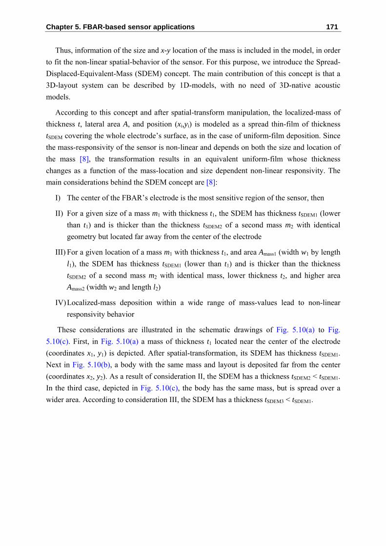
Chapter 5. FBAR-based sensor applications 171
Thus, information of the size and x-y location of the mass is included in the model, in order to fit the non-linear spatial-behavior of the sensor. For this purpose, we introduce the Spread-Displaced-Equivalent-Mass (SDEM) concept. The main contribution of this concept is that a 3D-layout system can be described by 1D-models, with no need of 3D-native acoustic models.
According to this concept and after spatial-transform manipulation, the localized-mass of thickness t, lateral area A, and position (xi,yi) is modeled as a spread thin-film of thickness tSDEM covering the whole electrode’s surface, as in the case of uniform-film deposition. Since the mass-responsivity of the sensor is non-linear and depends on both the size and location of the mass [8], the transformation results in an equivalent uniform-film whose thickness changes as a function of the mass-location and size dependent non-linear responsivity. The main considerations behind the SDEM concept are [8]:
I) The center of the FBAR’s electrode is the most sensitive region of the sensor, then
II) For a given size of a mass m1 with thickness t1, the SDEM has thickness tSDEM1 (lower than t1) and is thicker than the thickness tSDEM2 of a second mass m2 with identical geometry but located far away from the center of the electrode
III) For a given location of a mass m1 with thickness t1, and area Amass1 (width w1 by length l1), the SDEM has thickness tSDEM1 (lower than t1) and is thicker than the thickness tSDEM2 of a second mass m2 with identical mass, lower thickness t2, and higher area Amass2 (width w2 and length l2)
IV) Localized-mass deposition within a wide range of mass-values lead to non-linear responsivity behavior
These considerations are illustrated in the schematic drawings of Fig. 5.10(a) to Fig. 5.10(c). First, in Fig. 5.10(a) a mass of thickness t1 located near the center of the electrode (coordinates x1, y1) is depicted. After spatial-transformation, its SDEM has thickness tSDEM1. Next in Fig. 5.10(b), a body with the same mass and layout is deposited far from the center (coordinates x2, y2). As a result of consideration II, the SDEM has a thickness tSDEM2 < tSDEM1. In the third case, depicted in Fig. 5.10(c), the body has the same mass, but is spread over a wider area. According to consideration III, the SDEM has a thickness tSDEM3 < tSDEM1.
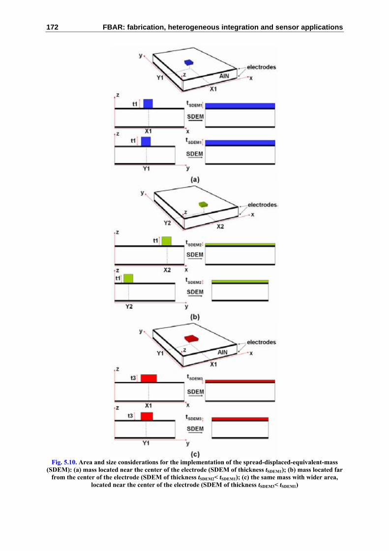
172 FBAR: fabrication, heterogeneous integration and sensor applications
Fig. 5.10. Area and size considerations for the implementation of the spread-displaced-equivalent-mass
(SDEM): (a) mass located near the center of the electrode (SDEM of thickness tSDEM1); (b) mass located far from the center of the electrode (SDEM of thickness tSDEM2< tSDEM1); (c) the same mass with wider area,
located near the center of the electrode (SDEM of thickness tSDEM3< tSDEM1)

Chapter 5. FBAR-based sensor applications 173
The spatial-transform functions involved in the SDEM dimensioning thus include mass location (x-y coordinates) and geometry (thickness, width, length) variables. According to the three considerations mentioned above, the 3D-equivalent model of the localized-mass sensor is built by modifying the classical 1D Mason’s model. Assuming perfect isolation between the FBAR and the substrate, said model is depicted in the circuit representation of Fig. 5.11, where the SDEM is the additional uniform-film layer deposited on the FBAR’s top electrode. Referring to this circuit, the analysis of the localized-mass sensor starts from the 1D-equation defining the electrical impedance Zin of the loaded-FBAR [28]:
( )( ) ( ) ⎟⎟
⎠
⎞⎜⎜⎝
⎛++++
++−×=
φφφφ
φφ
ω 2sin12cos2sincostan11 2
233
0 BTBT
BTin ZZjZZ
jZZkCj
Z (5.7)
Where φ is the half phase across the piezoelectric plate, k332 is the piezoelectric coupling
coefficient, C0 is the parallel-plate capacitance, and ZT and ZB are normalized acoustic impedances at the piezoelectric layer boundaries. In the localized-mass sensor’s model, the SDEM is included in the ZT impedance, as depicted in Fig. 5.11.
Fig. 5.11. Modified Mason’s equivalent-circuit mode of the localized-mass sensor, including the SDEM
circuit element
When seen from the top-electrode-to-SDEM interface, the input load impedance of the SDEM ZMASS is expressed by:
⎟⎟⎠
⎞⎜⎜⎝
⎛+
+×=
massairLmass
massmass
massmass
airLmass
MASS jZZjZZ
ZZφφφφ
sincossincos
0
00 (5.8)
Where Z0mass is the characteristic acoustic impedance of the mass, ZL
air is the input load impedance seen by the mass at the air interface, and φmass is the acoustic-wave phase across the SDEM layer. Since the SDEM is deposited on the FBAR’s top electrode, it finds low acoustic impedance at the air interface, thus simplifying the value of ZMASS in equation (5.8) to:

174 FBAR: fabrication, heterogeneous integration and sensor applications
massmass
MASS jZZ φtan0 ×= (5.9)
Where φmass depends on the wave vector κ and the thickness of the SDEM tSDEM by:
SDEMmass t×= κφ (5.10)
Where tSDEM is a non-linear function of the thickness t, the width w, the length l, and the location coordinates (xm, ym) of the deposited mass; and on the FBAR’s electrode area A, too. Final calculation of the electrical impedance Zin of the loaded-FBAR requires recursive calculation of ZT and ZB as it was done for the non-loaded FBAR discussed in section 3.5.5. Regarding the spatial location of the mass and its effects on the tSDEM function, the findings of previous work on the amplitude distribution of longitudinal-mode crystal resonators were used to model the 3D-topography of the sensor [19-20]. This is directly related to the location-dependent responsivity of the sensor. The graphics of Fig. 5.12(a) and Fig. 5.12(b) show the 2D-amplitude distribution when the mass is deposited on the center and on a lateral location of the electrode. The 3D-plot of Fig. 5.12(c) is an alternative view illustrating the non-linear nature of the sensor’s responsivity.
Fig. 5.12. Amplitude distribution of the localized-mass sensor’s responsivity: (a) 2D-topographic profile for mass deposition on the center of the electrode; (b) 2D-profile when the mass is deposited on a lateral
side of the electrode; (c) 3D-topographic representation of the profile in (a)

Chapter 5. FBAR-based sensor applications 175
Both the experimental and SDEM modeling results are compared in Fig. 5.13. According to consideration IV on SDEM modeling, the curves of Fig. 5.13(a) show the analysis results after localized-mass deposition on the center of the top electrode. In this case, the deposited masses have different sizes and identical mass. In a second study and according to consideration III, all the samples were configured with the same size (Amass= w×l) and different thickness t, in order to change the mass. The conclusions of this study are presented in Fig. 5.13(b). These results show good agreement between experimental and modeling data. Future refinement of the SDEM model will allow the combined analysis of mass, size and location of the localized-mass deposition.
Finite-element modeling of the localized-mass sensor In parallel to analytical modeling, FEM analysis of the mass-sensor system was
implemented in ANSYS ® in close collaboration with the IEF (Paris, France). Different locations and geometry of the localized-mass were configured in the model, in order to analyze the harmonic response and the mode-shaping dependence on the mass-loading configuration. The model considered non-homogeneous element-definition and meshing, with and without mass, in order to eliminate the frequency-shift due to meshing-related noise.
Fig. 5.13. Experimental and SDEM modeling results: (a) Frequency change against size of the localized-
mass (constant mass of 3.6×10⁻¹²g, different thickness and area to preserve the mass); (b) Frequency change as a function of the amount of mass (same area, different thickness, in order to change the mass).

176 FBAR: fabrication, heterogeneous integration and sensor applications
Fig. 5.14. Harmonic analysis for meshing evaluation of the finite-element-modeling of un-loaded FBARs
(no difference among the meshed models is observed)
Thus, the same un-loaded FBAR model with meshing configurations only differing on the smallest-sized element position was analyzed and the results of the harmonic analysis observed in the curves of Fig. 5.14. As it can be seen, the amplitude curves are identical among them for the different meshing configurations. This demonstrates independence of the analysis with respect to the meshing, which is critical to subsequent mass-loading analyses.
Once the meshing-dependent noise is controlled in the model, localized-mass deposition with different configurations was modeled. Masses with the same geometry and located in different positions of the electrode were included in the model, the center and the lateral regions of the electrode being the mass-deposition locations. An electrode of area 50μm×70μm was configured in the finite-element model. The curves of Fig. 5.15 show that the resonance frequency value is sensitive to the location in which the mass is deposited, the highest frequency shift obtained for the case of the center-located mass deposition. These results were compared to experimental characterization data, as observed in the plot.
Fig. 5.15. Frequency response sensitivity to different-located mass deposition (the distance in the inset is
the mass location with respect to the electrode’s center).

Chapter 5. FBAR-based sensor applications 177
This comparison evidences that the location of the mass is a key factor affecting the resonance frequency, the center of the electrode being the most sensitive area to frequency changes. At its time, this analysis coincides with the 3D topographic representation of the SDEM of Fig. 5.13.
Another contribution of the FEM analysis has been the evaluation of the mode-shaping dependence on the mass location. Given the resonance frequencies found in the harmonic analysis described above, modal analysis of the sensor was carried out. In this way, the mechanical displacements of the electrode for each frequency and mass location were calculated. The topographic model images of Fig. 5.16 show how the mode-shaping is modified when the mass is deposited on different positions of the electrode.
These results coincide with the analytic modeling results and with the conclusions of previous works on the amplitude distribution at resonance. Experimental analysis of the mode-shaping will allow future contrasting of the FEM and analytic results, by means of AFM techniques implementation [22-23].
Analytic and finite-element modeling confirmed the location and mass-layout dependence on the sensor’s responsivity. Future work should include further analytical and experimental evaluation of mode-shaping, based on topographic study of the electrode at resonance.
Fig. 5.16. Mechanical displacement of the FBAR after localized-mass deposition (ANSYS): (a) no mass
deposited; (b) 2.0μm×2.0μm-sized mass (center); (c) the same mass, located 10 μm away from the center of the electrode; (d) the same mass, located 20 μm away from the center of the electrode; (e) the same mass,
located 30 μm away from the center of the electrode

178 FBAR: fabrication, heterogeneous integration and sensor applications
5.2 The FBAR as a mechanical sensor In the previous section, a physical sensor application of FBAR was studied. Under
appropriate operating conditions and FBAR fabrication processes, the mass sensor can also be used in chemical-particle detection (although working as a physical sensor based on the mass-loading principle). In both cases, its high sensitivity reports performance sensing advantages against similar technologies. Also, FBARs operate at high frequencies with low power consumption. In regard of these features, the FBAR technology would have the potential of being a detection means for high-sensitivity mechanical sensors. In such a case, would the FBAR be able to perform high-frequency piezoelectric detection when operating in a mechanical sensing application? Which would be the involved fabrication technology? Is it compatible with current-FBAR processes? To answer these questions, we have initiated an exploratory work on mechanical-sensor applications. Different micro-machined structures were developed, intended for acceleration and force detection.
Looking into the fundamental equations of piezoelectricity, which we again reproduce here for convenience, illustrates the operating principle of an FBAR-based mechanical sensor:
3333333
3333333
ETdD
EdTsST
E
⋅+⋅=
⋅+⋅=
ε (5.11)
Where S is the strain matrix describing the deformation of the crystal, sE is compliance matrix (reciprocal of the stiffness matrix), T is stress matrix, d is charge-form piezoelectric constant matrix, E is electric field applied to the resonator, D is electric density displacement matrix, and εΤ is permittivity of the piezoelectric material [29]. If a mechanical force is applied to the FBAR’s structure, an added strain will superpose to the previous-field conditions, thus modifying the overall stress, electric field and displacement conditions. To our extent, this is the inverse effect to that occurring at DC-biasing of FBARs (where the added electric field changes the previous strain, stress and electric displacement conditions). Based on these assumptions, different movable structures comprising FBARs were designed. Thus, the FBAR is expected to suffer from mechanical deformation when said structures are exposed to external forces. First, FBAR-based accelerometers are discussed in the next section.
5.2.1 FBAR-based accelerometer Miniature accelerometers are a popular application of MEMS-based sensors. Nowadays,
current MEMS-accelerometer technologies use capacitive [30], piezoresistive [31], field-effect-transistor (FET) [32], or piezoelectric [33] detection mechanisms, among others. The technologies required to fabricate these accelerometers implement back-side bulk micro-machining of the silicon substrate [34], surface micromachining [35, 36], or combination of the same [30]. The main body of the accelerometer’s structure is usually silicon, which is

Chapter 5. FBAR-based sensor applications 179
etched to define the seismic mass and the beams supporting the same to the chip. In most of these technologies, the sensing device is deposited or implanted to the beams or to the mass, as for example the piezo-resistance in piezoresistive accelerometers. On the other hand, resonant and non-resonant accelerometers can be found. However, piezoelectric-based accelerometers are usually of the second kind: deformation of the acoustic layer of the sensor is read-out as a DC voltage proportional to the strain. To our extent, no previous work on FBAR-based resonant accelerometers exists. This fact and the previous experience of CNM on designing and fabricating micro-machined accelerometers have motivated the development of FBAR-based accelerometers.
The FBAR-based accelerometer is a micro-electromechanical system, whose acceleration-sensing devices are FBARs. The mechanical structure of the accelerometer is comprised by a movable, seismic mass, supporting beams and embedded-FBAR devices (Fig. 5.17). Each one of the supporting beams embeds a micro-machined FBAR, whose resonant frequency changes when the beam bends due to the application of acceleration forces to the seismic mass.
Fig. 5.17. The embedded-FBAR accelerometer: (a) upper view of a quad-beam accelerometer; (b) cross-
sectional view of one of the beams with FBAR.

180 FBAR: fabrication, heterogeneous integration and sensor applications
Both the mass and the beams are made of silicon, although in a variation of the process each beam can be an FBAR in itself. At its time, the FBAR is fabricated and micro-machined on top of the supporting beam. Fig. 5.17(a) depicts an upper view schematic of the embedded-FBAR accelerometer concept. In this figure a quad-beam accelerometer is shown, each beam of the same embedding an FBAR device. A more detailed view of the embedded-FBAR with beam and seismic mass can be obtained in the drawing of Fig. 5.17(b), which is cross-sectional view of one of the beams represented in Fig. 5.17(a). As it is observed, both the beam and the FBAR have been micro-machined, the FBAR being processed on the beam’s structure in order to provide the resonator with an air gap.
Acceleration forces applied to the seismic mass cause a strain in its mechanical configuration. Since the mass and the beams are mechanically coupled, this strain is transmitted to the beams and to the FBARs embedded on them. Due to the piezoelectric effect, this strain of the piezoelectric, acoustic layer of the FBAR produces a charge displacement in the piezoelectric, causing a shifting in the resonant frequency of the resonator. Thus, the electrical charge displacement within the crystal and the resonant frequency of the FBAR will be proportional to the magnitude and orientation of the acceleration force applied to the mass.
As a difference to previous MEMS accelerometers, the micro-machining technology of the embedded-FBAR accelerometer involves not only the seismic mass and the supporting mass, but also the FBAR-based sensing device. In this sense, back-side bulk micro-machining is performed to release the seismic mass and the beams of the accelerometer. On the other hand, the FBAR-sensor manufacturing requires front-side micro-machining to complete its releasing. This provides mechanical isolation of the same to the silicon substrate, allowing for high-quality factors and frequency sensitivity. In the following section, we present a complete description of the process and fabrication technologies of the accelerometer and its embedded-FBAR sensing devices.
5.2.2 Fabrication technology As it was explained in the foregoing section, the accelerometer is composed by a seismic
mass, supporting beams and FBAR-based sensing devices. The FBAR has been released by means of front-side reactive-ion-etching (RIE) of the silicon-made beams of the accelerometer. RIE is also carried-out to release the seismic mass and the beams –which are made of silicon, too–, the process being completed by back-side deep- reactive-ion-etching (DRIE) of the silicon substrate [37].
The complete process is depicted in the schematic drawings of Fig. 5.18(a) and Fig. 5.18(b), the same being cutaway views of the device of Fig. 5.17(a) cut along the line A-A’. Two cases are considered in this process: the “thick mass” and the “thin-mass” accelerometer. The thick-mass device will have increased sensitivity, compared to the thin-mass

Chapter 5. FBAR-based sensor applications 181
accelerometer. Also, the thickness of the supporting beams and the size of the mass will affect the sensitivity of the device, among other aspects. In both cases, the FBAR is fabricated on the silicon wafer – step I in Fig. 5.18(a) and Fig. 5.18(b)–. Said FBAR is comprised by top and bottom metal electrodes and piezoelectric, acoustic layer. Both the electrodes are made of platinum/titanium (Pt/Ti) layer (150/30nm thick). The piezoelectric layer is implemented as a sandwiched aluminum nitride (AlN) membrane (1μm-thick), sputtered on top of the bottom electrode layer. Prior to deposition of the first metal layer, an isolating silicon oxide layer is deposited on top of the silicon substrate to provide electrical isolation and diminish RF losses. Next, back-side bulk-micromachining is performed in order to fabricate the supporting beams and the seismic mass of the accelerometer, as depicted in the step II of Fig. 5.18(a) and Fig. 5.18(b). This process is carried out by means of DRIE and is completed according to the desired thickness for the beams and the mass. As depicted in the drawings, the same technological process is implemented in both the thin and the thick seismic-masses. However, the corresponding photolithography masks are different for one case or the other one. In the case of the thin-mass (step I in Fig. 5.18(b)), the seismic mass and the supporting beams have the same thickness. In such a case, this mask should cover the whole area comprising both the mass and the beams. As a result, the central area of the accelerometer –beams and seismic mass– will have the same thickness of the beam (we have chosen a mass’ thickness of 80μm). On the other hand, the thick-mass accelerometer exhibits seismic mass and supporting beams with different thicknesses (step II in Fig. 5.18(a)). If a single photolithography mask is employed, the thickness of the seismic mass is equal to the wafer’s thickness (we implemented 500μm-thick silicon wafers for this application), whereas the supporting-beam’s thickness is chosen by the designer (in the general case, the thickness of the beams is controlled by the DRIE processing time, given an etching rate, previously known).
Fig. 5.18. Embedded-FBAR accelerometer: (a) heavy, thick-mass and (b) light, thin-mass device. Both
implementations follow the same fabrication process for the patterning of: (I) the FBAR, (II) supporting beams and seismic mass, and (III) the FBAR cavity and supporting beams

182 FBAR: fabrication, heterogeneous integration and sensor applications
In the first implementations of the accelerometer we chose 80μm-thick supporting beams, the heavy mass having a thickness of 500μm. The back-side and front-side etching times are controlled to complete the process at both sides of the wafer.
Finally, releasing of the embedded-FBAR devices and definition of the supporting beams are performed by means of front-side reactive-ion-etching (RIE). Also, the RIE performs the front-side etching of the silicon around the supporting beams, thus allowing the release of the seismic mass by its lateral sides and providing a freely-moving seismic mass only supported by the beams, as depicted in the step III of Fig. 5.18(a) and Fig. 5.18(b). The set up of the RIE is the same of that previously described in chapter 2 (SF6 and O2 atmosphere in the RIE-machine chamber, among other conditions).
Depending on the process duration and the relative thickness of the supporting beams and the FBAR, partial or total etching of the beam in the area underneath the FBAR can be accomplished. Since the embedded-FBAR is assumed to be small enough compared to the size of the beam, the selection of a specific etching time to perform a through-hole in the beam is not relevant for the reliability of the whole beam structure.
Fig. 5.19. Quad-beam, embedded-FBAR accelerometer after manufacturing: (a) Overall structure detailing the four embedded-FBARs, corresponding beams and seismic mass ((Optical image); (b) front-
side (SEM image); (c) Detailed view of one of the embedded FBARs; (d) back-side (SEM image)

Chapter 5. FBAR-based sensor applications 183
Nevertheless, what is really important is to adjust the front-side and back-side etching times in order to completely release all the structures, without taking an excessive amount of etching time. The optical and SEM images of Fig. 5.19 show different views of the quad-beam embedded-FBAR accelerometer fabricated according to the above-described manufacturing process. In this image, a quad-beam accelerometer with thick-mass is observed. The dark region around the mass and the supporting beams is completely released from the substrate by means of front-side RIE. A couple of Si clamps supporting the chip can be seen in the lateral sides of the accelerometer: by cutting or breaking these clamps the chip can be de-attached from the wafer. For this reason, these arms have been designed to be easily broken, even with manual operation. In Fig. 5.19(a) and Fig. 5.19(b), the FBARs are shown with their corresponding pad connections. These pads are intended for wire-bonding interconnection, for read-out and characterization purposes. In Fig. 5.19(c) a detailed view of the FBAR and the area underneath it are shown. Also, the electrode connections and the Si of the supporting beam are seen. This FBAR has a length of 100 μm, a width of 40 μm, and thickness of 1 μm. Fig. 5.19(d) shows another interesting bird’s eye view of the accelerometer, taken from the back-side of the chip. In this image, the thickness of the seismic mass (on the central region) can be contrasted with that of the thinner supporting beams (this is an example of the “thick-mass” case).
A second example of fabricated accelerometers is the double-beam device shown in the SEM images of Fig. 5.20. Front-side (Fig. 5.20(a)) and back-side (Fig. 5.20(b)) images of the whole chip offer a complete sight of the shape of the double-beam accelerometer. The same clamping devices are fabricated on the lateral side of the chip to facilitate its manipulation. Fig. 5.20(c) shows a detailed view of one corner of the seismic mass, close to one of the FBARs. It can be appreciated the sharp definition of the structure. This image contrasts with the back-side general view of the device presented in Fig. 5.20(d), in which no step between the supporting beams and the thin-mass is observed.
5.2.3 Low-frequency characterization and modeling Low frequency and high frequency characterizations were performed on fabricated quad-
beam accelerometers. As a moving structure, its geometry and operating principle are the main factors limiting the bandwidth and applications of the accelerometer. In order to evaluate these limits, the resonance modes of the different elements of the device’s geometry, i.e. the seismic mass, the beams and the sensing device have to be analyzed. First, the low frequency vibration modes of the accelerometer –including the fundamental mode of the embedded-FBAR– were analyzed. Finite-element-modeling and experimental S-parameter data were compared and the bandwidth of the accelerometer evaluated. According to Ansys ® simulations, the fundamental mode of the seismic mass-beam system was found at a frequency of 3 kHz.

184 FBAR: fabrication, heterogeneous integration and sensor applications
Fig. 5.20. Double-beam embedded-FBAR accelerometers: (a) front-side; b) back-side (thick-mass); (c)
back-side (detail of the thick-mass); (d) back-side (thin-mass)
Good agreement between simulation and experimental data on the embedded-FBAR’s fundamental mode was obtained. The picture in Fig. 5.21(a) shows the Ansys ® representation of the shape of the embedded-FBAR when resonating at 800 kHz. This frequency corresponds to the fundamental mode, according to modal analysis, and is also in accordance to the analytical model for a clamped-clamped beam [38]:
A
EIl
f nn ρ
απ 2
2
21
= (5.12)
Where fn is the n-mode resonance frequency, E is the Young’s modulus, ρ is the density, l is the beam length, A = wh is the cross-section area, w and h being the width and thickness, respectively, and I = wh3/12 is the moment of inertia. The coefficient αn depends on the mode number. For the first mode, leading to the fundamental natural frequency f1, it is α1 = 4.73 [39]. For the FBAR of Fig. 5.19(c) with dimensions l= 100μm and h= 1μm; and mechanical constants ρ= 3,260 kg/m3 and E= 200GPa, f1 is calculated to be 805 kHz. In Fig. 5.21(b), low-frequency S-parameter characterization details the frequency response around the first fundamental mode (n= 1).
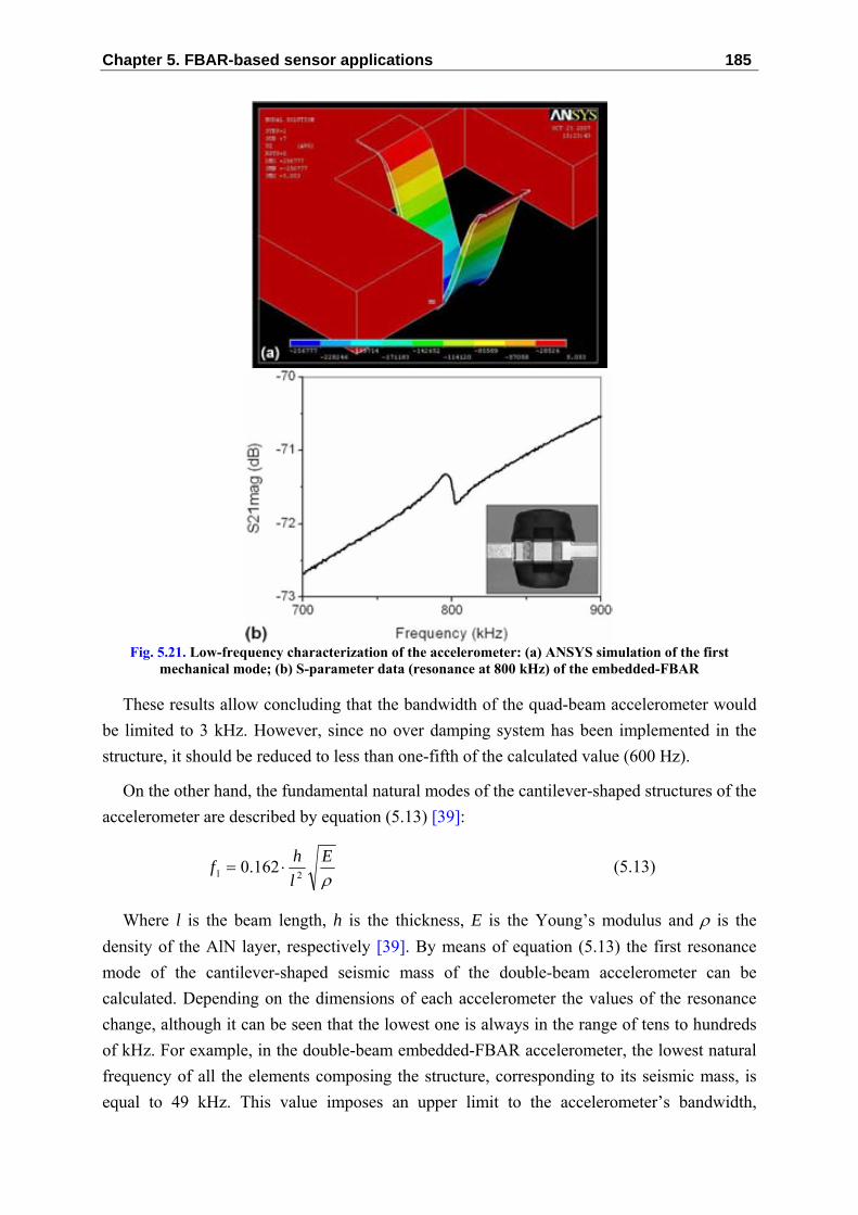
Chapter 5. FBAR-based sensor applications 185
Fig. 5.21. Low-frequency characterization of the accelerometer: (a) ANSYS simulation of the first
mechanical mode; (b) S-parameter data (resonance at 800 kHz) of the embedded-FBAR
These results allow concluding that the bandwidth of the quad-beam accelerometer would be limited to 3 kHz. However, since no over damping system has been implemented in the structure, it should be reduced to less than one-fifth of the calculated value (600 Hz).
On the other hand, the fundamental natural modes of the cantilever-shaped structures of the accelerometer are described by equation (5.13) [39]:
ρE
lhf 21 162.0 ⋅= (5.13)
Where l is the beam length, h is the thickness, E is the Young’s modulus and ρ is the density of the AlN layer, respectively [39]. By means of equation (5.13) the first resonance mode of the cantilever-shaped seismic mass of the double-beam accelerometer can be calculated. Depending on the dimensions of each accelerometer the values of the resonance change, although it can be seen that the lowest one is always in the range of tens to hundreds of kHz. For example, in the double-beam embedded-FBAR accelerometer, the lowest natural frequency of all the elements composing the structure, corresponding to its seismic mass, is equal to 49 kHz. This value imposes an upper limit to the accelerometer’s bandwidth,

186 FBAR: fabrication, heterogeneous integration and sensor applications
although a frequency lower than the fifth part of the resonance frequency is chosen to prevent the amplitude rise due to the resonance [40]. In this example, an operating bandwidth of less than 10 kHz should be a practical limit to the accelerometer’s response.
Comparing the high-frequency, longitudinal-mode resonance of the FBAR -2.4GHz- with those of the fundamental modes of the accelerometer’s structure –kHz, even MHz-, the relationship between the piezoelectric and mechanical constraints of the system is to be determined, in order to evaluate the sensitivity of the accelerometer.
5.2.4 High-frequency characterization set-up and results The longitudinal-mode resonance frequency of the FBAR was measured for static
acceleration conditions, i.e. in the presence of gravity. In this way, the accelerometer was mounted on a rotating fixture and the resonance frequency measured for different inclination angles with respect to the horizontal plane (+1g acceleration). Thus, the static response of the accelerometer is evaluated. For this purpose, a set-up comprising a supporting table, a rotating wheel, a microwave network analyzer and the packaged accelerometer chip was prepared, as depicted in the schematic drawing of Fig. 5.22. First, the accelerometer was packaged, by means of bonding and gluing of the chip to a printed-circuit-board (PCB), the same comprising two RF ports with SMA connectors, in which the ports A and B of a network analyzer were connected. The PCB with the chip and connectors was attached to the rotating wheel, which at its time was fixed to the supporting table in order to control the accelerometer’s rotation. Finally, the RF ports of the PCB were connected to the network analyzer, and different angles of the rotating wheel were tested.
Fig. 5.22. Characterization set up of the static-acceleration response of the embedded-FBAR
accelerometer

Chapter 5. FBAR-based sensor applications 187
For each inclination of the FBAR-sensor, the transmission and reflection scattering-parameters were measured and the resonance frequency of the FBAR evaluated. Angular positions of the rotating wheel from -90 to +90 degrees were tested, in 10-degree steps. The 90-degree angle θ is defined with respect to the plane parallel to the supporting table (horizontal plane), and with the FBAR in the position depicted in Fig. 5.18 (i.e. FBAR up respect to the beam). In this position, the sensor and the seismic mass experiment an acceleration force equal to +1g (+9.8 m/s2). In the -90-degree case the FBAR is also in the plane parallel to the supporting table, but it is oriented down respect to the beam (FBAR face to the table). Characterization results of the quad-beam accelerometer are shown in the frequency-to-inclination plot of Fig. 5.23. A frequency-to-static-acceleration sensitivity of 200 kHz/g is evaluated, after sinusoidal fitting of the measured resonance-frequency values. Previous works on piezoresistive accelerometers by Aikele et al. (2001) and Ferrari et al. (2005), demonstrated frequency-to-static-acceleration sensitivities of 70Hz/g and 35Hz/g, respectively [41-42].
Compared to these works, the embedded-FBAR accelerometer exhibits a sensitivity that is more than 2,000 times higher [43]. However, the resonance frequency of the sensing device is also several orders of magnitude higher than that of the reference piezoresistive devices. Actually, if we evaluate the Δf/f0 factor of both technologies for the static-acceleration case, we find a 1×10⁻³ value for the piezoresistive accelerometer, which is one order of magnitude better than the 1×10⁻⁴ value of the embedded-FBAR accelerometer.
Fig. 5.23. Experimental characterization of the quad-beam embedded-FBAR accelerometer: resonance
frequency versus the inclination angle of the device (±90º correspondence to ±1g)

188 FBAR: fabrication, heterogeneous integration and sensor applications
Hence, the impact of a high-frequency sensing device –the embedded-FBAR– in the performance of an accelerometer is a feature that has still to be evaluated, in order to determine the competitive advantages of this technology.
Future developments of this work will be oriented to perform dynamic acceleration measurements. By using a shaking table and an improved measurement set up, the noise floor and bandwidth evaluation of the accelerometer will be carried out. Also, optimization of the mechanical configuration and geometry of the accelerometer is to be done. Optimized accelerometer’s design will allow the survey of new FBAR-based accelerometer applications and the integration with read-out circuits.
5.2.5 Other FBAR-based accelerometer concepts and devices Up to now, the accelerometer technology and fabrication process embedding an FBAR into
the supporting beams structure have been discussed. However, other concepts for the FBAR-based accelerometers were conceived too. Among them, those devices having FBAR-made supporting beams are presented now. Although their layout, beam materials, and micro-machining conditions (etching time for RIE) are different, the operating principle and fabrication technology are the same for both kinds of accelerometers.
In these concepts, FBAR-based accelerometers implement one or more FBAR-made stripes performing the supporting-beam functionality. Hence, the sensing devices and the supporting beams are the same structures, which are also micro-machined according to the same size and process requirements of the embedded-FBAR accelerometers. As in previously-described implementations, the seismic mass is also made of silicon, although the fabrication process of these devices is slightly different, as depicted in the schematic drawing of Fig. 5.24.
As in the embedded-FBAR accelerometer’s concept already described, we can also have the accelerometers with thin and thick masses. According to this process, the FBAR-made beams are fabricated in the step I, as in the standard FBAR fabrication process (electrodes and AlN deposition and patterning). In the step II, the seismic mass is patterned by means of back-side DRIE. Finally in step III, the FBAR-made supporting beams are released by front-side RIE. The etching times of both DRIE and RIE have to be adjusted to complement each other in the purpose of releasing the FBARs, i.e. the beams.

Chapter 5. FBAR-based sensor applications 189
Fig. 5.24. The FBAR-beam accelerometer’s fabrication process
The layout of this kind of FBAR-based accelerometers may vary notoriously from one device to another. However, due to the reduced thickness of the supporting beams (1-2 μm, coinciding with the FBAR’s thickness), improved sensitivity is expected for this kind of accelerometers. Concerning the design of the FBAR, process and functional considerations are to be taken into account. One of the main design issues was to choose the length and width of the beams, in order to provide the beam with flexibility and, at the same time, to etch the structure within reasonable processing times. First, a long beam allows enough strain, thus achieving improved sensitivity (too much length leads to fragility of the structure, however). On the other hand, wide beams ensure robustness of the system, but at the cost of increased etching time (alternatively, narrow beams lead to fragility, although the etching time is reduced). Thus, the design solution proposes a trade-off between these issues, by implementing the beam/sensing devices as one or more FBAR-made stripes. Each stripe is 40μm-wide and is electrically connected to the other stripes, the overall area of the electrode being the sum of the individual areas of each beam/sensing device. Various realizations of the FBAR-beam accelerometer are shown in the images of Fig. 5.25, the main difference between them being the number of stripes and mass geometry. For a 40μm-wide stripe the front-side, RIE-based etching time is around 120 minutes (lateral etching: 20μm, vertical etching: 80μm).
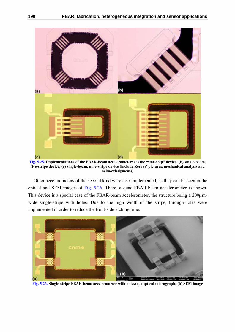
190 FBAR: fabrication, heterogeneous integration and sensor applications
Fig. 5.25. Implementations of the FBAR-beam accelerometer: (a) the “star-ship” device; (b) single-beam, five-stripe device; (c) single-beam, nine-stripe device (include Zervas’ pictures, mechanical analysis and
acknowledgments)
Other accelerometers of the second kind were also implemented, as they can be seen in the optical and SEM images of Fig. 5.26. There, a quad-FBAR-beam accelerometer is shown. This device is a special case of the FBAR-beam accelerometer, the structure being a 200μm-wide single-stripe with holes. Due to the high width of the stripe, through-holes were implemented in order to reduce the front-side etching time.
Fig. 5.26. Single-stripe FBAR-beam accelerometer with holes: (a) optical micrograph; (b) SEM image

Chapter 5. FBAR-based sensor applications 191
5.2.6 FBAR-based force sensors Atomic force microscopy (AFM) allows high resolution surface imaging by scanning a
sharp tip over a surface while controlling the interaction force between tip and surface [44]. AFM uses micro-machined cantilevers with a sharp tip at the apex as a force sensor to detect tip-sample interactions. Using micromachining technologies, the dimensions of cantilevers can be tuned to optimize sensitivity, resonant frequency, elastic constant and other properties [45]. Both the cantilever and the tip are usually made of polysilicon, although other materials, like quartz, are implemented as well [46]. Examples of AFM probes made of crystalline silicon are observed in the SEM images of Fig. 5.27.
In AFM systems, force detection is performed by measuring the deflection of the cantilever when it is attracted by the sample. This measurement is carried out by means of complex optical or interferometer techniques, the set up comprising laser, optical detectors, signal generators and lock-in amplifiers, among others [23]. In this work, a new detection method for AFM applications is proposed: based on the same operating principle of FBAR-based accelerometers, deflection of an FBAR-made cantilever will cause shifting of the resonance frequency of the FBAR.
The concept of the FBAR-based force sensor for AFM applications is illustrated in the schematic drawings of Fig. 5.28(a) and Fig. 5.28(b), where two cases are differentiated. In the configuration of Fig. 5.28(a), the FBAR is embedded on the cantilever’s structure, which can be made of silicon and has a tip close to its vertex. When the probe and the sample approach each other, the cantilever deflects, thus bending the FBAR and adding stress to the piezoelectric layer. This deflection is detected as a change of the resonance frequency of the FBAR, directly proportional to the probe-sample attraction forces. In the second configuration, shown in Fig. 5.28(b), the cantilever and the tip are the same V-shaped structure, which is fabricated according to the FBAR process.
Fig. 5.27. AFM probes made of crystalline silicon: (a) SEM micrographs of a typical AFM probe-chip, with shaft diameter ~3.8 μm, apex radius ~10 nm, and vertex angle ~10°. Cantilevers thickness is 1.5 μm, width is 25 μm and length is 250 μm, 350 μm and 50 μm (from left to right).; (b) detailed view of one tip
(after [45]: Villanueva et al., 2007)

192 FBAR: fabrication, heterogeneous integration and sensor applications
Fig. 5.28. Concept of the FBAR-based AFM force detector: (a) first configuration: the FBAR is embedded on the Si cantilever’s structure; (b) second configuration: cantilever and tip are a V-shaped FBAR. In
both cases, the probe-sample attraction causes deflection and frequency shifting of the FBAR.
As observed in the figure, the V-FBAR cantilever deflects when attracted by the sample, thus changing its resonance frequency. The fabrication technology, operation, and detection principles are the same for both configurations. A combination of RIE and DRIE is required to release both the cantilever and the FBAR (which are the same structure in the second case).
Although several AFM-probe fabrication technologies exist, the development of FBAR-based force sensors are still at early stages of analysis and design. For this reason, we have designed and fabricated structures different-shaped with the aim of force-sensing concept’s demonstration. The fabrication process is also based on front-side RIE and back-side DRIE. Two kinds of FBAR-based force sensors were conceived. The first kind embeds an FBAR as sensing device close to a tip-shaped silicon structure. The FBAR is released by means of front-side RIE, whereas the silicon is etched by both RIE and back-side DRIE. The SEM and optical micrographs of Fig. 5.29 illustrate the concept of fabricated devices of the first kind.
The second type of force sensors comprises an FBAR-made tip as the sensing device. Triangular-shaped tips were designed and fabricated according to the same technological process described for the first type of sensors. Tips of lengths between 5 and 50 μm, and widths of 5-20 μm were implemented. The AlN layer and the metal electrodes are 1um-thick and 180 nm-thick, respectively. Two examples of the FBAR-made tip can be seen in the

Chapter 5. FBAR-based sensor applications 193
optical micrographs of Fig. 5.30. The residual stress of the AlN layer presumably causes the bending observed on the tips.
Both kinds of sensors could be implemented in future AFM applications if a force tip is deposited on or grown near to the FBAR [45]. In this application, the tip is placed above the analyzed sample to perform force interaction, and the FBAR detects the force intensity by reading out of the resonance frequency’s variation.
Fig. 5.29. Force sensors with embedded-FBAR sensing device: (a-b) general view (SEM); (c-d) detailed
view of the FBAR-sensors, close to the tip (optical micrograph)
Fig. 5.30. Force sensors made with FBAR-sensing tip: (a) small size; (b) big size

194 FBAR: fabrication, heterogeneous integration and sensor applications
At this time, we have implemented various FBAR-based force-sensor structures, with the aim of concept’s demonstration and evaluation of the manufacturing feasibility. Future characterization and FEM analysis of these structures will determine the ultimate applications and possibilities of the FBAR-based force-sensor concept.
5.3 The contact-free acoustic resonator concept Up to this section, longitudinal-mode FBARs have been the main concern of this work.
However, FBARs and other acoustic-wave resonators can operate in non-longitudinal resonance modes, or they can be designed with a process differing from the traditional metal-piezoelectric-metal stack configuration. A second group of BAW resonators is that of lateral-field bulk acoustic wave devices (LFBAR). Although the resonant frequency of LFBAR is usually lower than that of FBAR, its layout and fabrication is simpler [47]. LFBARs can operate in a quasi-surface acoustic wave regime, the propagation of the wave being of the Lamb type. In the Lamb-mode, a combination of surface and bulk acoustic wave propagations takes place. Another technological option is to have a shear-mode propagating through the bulk of the piezoelectric layer. The simplest layout for an LFBAR is a co-planar electrode array, as in SAW devices, which is depicted in Fig. 5.31.
More recently, several variations of the classical BAW stack-structure concerning with resonance modes, shape of resonator, and fabrication process have also been proposed, in order to accomplish specific applications. For example, a ring-shaped contour-mode aluminum nitride (AlN) piezoelectric resonator for UHF applications between 223 and 656 MHz has been presented [48]. On the other hand, different sensors based on piezoelectric resonators have also been studied: a lateral extensional mode (LEM) piezoelectric resonator for mass sensing at 60 MHz [49], or FBARs operating in shear mode for bio-sensing [50], to mention two examples. Fig. 5.32 shows the ring-shaped and brick-shaped LEM resonators based on AlN.
In this section and under the concept of lateral-field device, a third application of the FBAR technology process is proposed. Hence, a contact-free thin-film acoustic resonator based on AlN is introduced.
Fig. 5.31. Lateral field FBAR (LFBAR): device layout and wave propagation

Chapter 5. FBAR-based sensor applications 195
Fig. 5.32. Lateral-extensional-mode (LEM) piezoelectric resonators based on AlN, ring-shaped and brick-shaped (after [48]: Piazza et al., 2005)
The concept of contact-free acoustic resonators was developed in the 70’s for quartz-based devices [51]. Two examples are the contact-less confined readout of quartz crystal resonator sensors [52] and the different-shaped devices operating in overtone-modes at 3 GHz [53]. In the first example, a back electrode is capacitively coupled to a separated tip electrode for contact-less readout of the resonance response of a thickness-shear mode quartz resonator sensor. In the second one, shear mode generation and excitation of the resonator is typically conceived by means of three-dimensional electrode structure not touching but surrounding the acoustic layer. The contact-free thin-film acoustic resonator introduced here is a quasi-two-dimensional co-planar structure, in which a central piezoelectric bar is located in-between two parallel-line metal electrodes (Fig. 5.33). Its geometry would make the contact-free resonator suitable for sensor applications in which no contact between the sensing element (the AlN bar) and the electrodes is desired. This could be the case of some chemical-detection systems.
This layout reduces the complexity of manufacturing, since the metal electrodes may be defined in the same process step. The isolating-and-energy-trapping well of Ballato et al. [53] is replaced here by a micro-machined-cavity in the surface of substrate, placed in a position that enables acoustic energy trapping. Separation between the co-planar electrodes and the acoustic layer is provided by photolithography processes. On the other hand, and compared to other previously-reported piezoelectric resonators [48-50], the contact-free thin-film acoustic resonator exhibits higher resonance frequencies, this feature being explained under the assumption of longitudinal-mode bulk resonance, in which the frequency mainly relies on the AlN layer’s thickness. This feature may be exploited to future RF MEMS and high-sensitivity sensor applications, as well. The acoustic layer is an aluminum nitride (AlN) bar of nominal thickness around 1μm.

196 FBAR: fabrication, heterogeneous integration and sensor applications
Fig. 5.33. Contact-free acoustic resonator process, showing (a) top view, (b) cross-sectional view (axis A-A’), and (c) SEM image of sample device. The co-planar structure allows for fabrication of electrodes A
and B in the same manufacturing step.
The metal electrodes are made of platinum/chromium (Pt/Cr), the whole co-planar structure being placed on top of a silicon oxide layer (SiO2) grown on top of silicon substrate. Said SiO2 layer is previously patterned to allow etching of a titanium (Ti) sacrificial layer. The volume occupied by the sacrificial layer is surface-micro-machined to provide the structure with a cavity containing part of the volume of the AlN bar, one of its ends being placed in a volume close to this cavity. The remaining end of the bar is in direct contact with the SiO2 layer.
The geometry of the contact-free acoustic resonator and silicon-well allows for energy trapping of electric field created in-between each metal electrode and the AlN acoustic bar. In this sense, the cavity etched on the silicon substrate traps the acoustic energy and improves the read-out capability of the device, because the coupling with the silicon substrate is reduced (and the Q-factor is improved). Two layout configurations of the contact-free thin-film acoustic resonator have been fabricated, the main differences being the length, width and thickness of the AlN bar, among others. In the first configuration the AlN-bar is 10μm-wide and 280μm-long, while the second one is 2.5μm-wide and 280μm-long. Also, the separation between the AlN bar and electrodes is different for each layout version, being of 7μm and 3μm for the first and second one configurations, respectively. It is to be noted that in both configurations the AlN bar has only one end of the same released on top of the air cavity, with suspended length over the cavity of 90μm and 40μm. The opposite end of the bar is clamped to the substrate (on top of the SiO2 layer).
S-parameter characterization of the contact-less acoustic resonator was carried-out, by means of a co-planar-probe RF measurement station and a microwave network analyzer –Agilent E5100A–. As a radiating structure, the contact-less acoustic resonator can be characterized in the same way as it is done for dipole antennas. Hence, impedance matching

Chapter 5. FBAR-based sensor applications 197
and return loss are key parameters in describing the bandwidth and performance of the dipole. The S11 parameter is the input reflection coefficient that better describes these aspects, and is therefore useful in analyzing passive dipole performance. An ideal match should provide S11= 0dB. A reference point to determine a matching network is S11 = -10dB. Therefore, desirable bandwidths (BW) includes frequencies where the magnitude of S11 ≤ -10dB [54].The design goal here is it to reach an equal value of |S11| than the one delivered by the generator, which is reached below this value (-10dB).
The curves plotted in Fig. 5.34 show the magnitude of measured scattering parameters for the layout group of resonators with lateral dimensions being 2.5μm-wide and 280μm-long, whose resonance frequencies of around 2.6 GHz can be observed. No significant frequency deviation was verified between the analyzed layout configurations. In Fig. 5.34(a) the magnitude of the S11 parameter is given: Although the insertion losses are low –near to 0dB–, return losses are still too low and far away from the -10dB reference value.
Fig. 5.34. S-parameter characterization of various contact-free acoustic resonators: (a) S11 parameter; (b) S21 parameter. All devices correspond to the layout group with geometrical configuration for the AlN bar
being 2.5μm-wide and 280μm-long.

198 FBAR: fabrication, heterogeneous integration and sensor applications
According to these results, further optimization of the device is required, in order to fit standard matching and bandwidth considerations in dipole performance. Other commonly used S-parameters in dipole characterization are S21, S12 and S22, which describe forward transmission, reverse transmission and output reflection, respectively. In Fig. 5.34(b) the magnitude of the S21 parameter shows the coupling level –i.e. forward transmission– between the two electrodes of the resonator. High-insertion losses of 30-40 dB and low quality factors of around 20 are observed. These figures are far from those obtained from standard FBAR geometries, the same having near-to-zero insertion losses and several-dB S21 peak-magnitudes figures. Again, improved electrode coupling is a matter of future developments in the geometry of the device. Nevertheless, characterization results demonstrate for the first time the contact-less excitation in FBAR devices.
Optimization tracks of the device would make it of possible interest in filter, reference oscillators or sensor applications. For example, the current layout asymmetry can lead to unfavorable energy distribution within the AlN. At this point, the electrostatic excitation energy distribution is not yet studied.
Fig. 5.35. Effect of the contact-free resonator’s location in the wafer: (a) S11 parameter; (b) sample device
under characterization with a co-planar probe station

Chapter 5. FBAR-based sensor applications 199
Fig. 5.36. Optimized, symmetric layout of co-planar contact-free acoustic resonators (future development)
This can explain the weakness, low return loss and high-insertion losses of the frequency response. A second study on the response of the resonator with respect to the position of the device in the wafer was also carried out. As observed in the plots of Fig. 5.35(a), a frequency variation occurs for different locations of the device. The farther the resonator is located from the center of the wafer, the higher the resonance frequency exhibited by the device (key: in the figure’s inset, the x,y duplet indicates a coordinate system, where 0-0 is the center of the wafer). This could be explained by the presumable thinning of the AlN bar, as it was previously discussed in section 3.7.1. The micrograph of Fig. 5.35(b) shows one device under characterization with the probe station.
New designs and future layout electromagnetic analysis based on CAD tools –like ADS ®– can be accounted as optimization actions. The layouts shown in Fig. 5.36 are some of the proposed design modifications, in order to provide increased symmetry to the device’s geometry and, presumably, more favorable energy distribution. Another layout-related aspect affecting the contact-free resonator’s performance is the coupling media between the AlN bar and the electrodes. As Lin et al. demonstrated for their solid-gap 160-MHz disk MEMS resonator, optimization of the lateral technology dimensions and coupling dielectric (nitride) leads to significant improvement of the frequency response, thus diminishing the insertion losses and the equivalent-circuit motional resistance values, at the cost of acceptable Q-factor reduction [55]. Mechanical and electrical issues concerning the GHz resonant frequency of contact-free acoustic resonator should be considered in this optimization.
The contact-free acoustic resonator may found possible application in high-frequency, no-contact sensing systems. For this purpose, the co-planar structure of this resonator prevents electrodes to be in contact with the analyzed substances, but only the active-sensing material -the AlN of bar-. With appropriate packaging and isolation of electrodes, coating of the AlN bar could be carried-out. At its time, coating of the bar may allow for sensing capabilities in wet or dry systems, as well. Layout optimization should be initiated in order to maximize the electrode-to-AlN-bar electrical coupling. As a consequence of the coupling optimization, an improvement of the quality factor is expected, too. Further analysis of optimized devices

200 FBAR: fabrication, heterogeneous integration and sensor applications
would allow the evaluation of feasible, future application-oriented implementations. Aspects to be studied are: the distance between the AlN bar and electrodes, the effects of packaging and/or isolation of electrodes, the geometrical configuration (length, width, and thickness), and the micro-machining of the AlN bar, among others.
5.4 Summary A variety of novel FBAR-based applications have been presented. In the first section, mass
sensor applications were studied. First, the sensitivity analysis of our FBARs in distributed-mass sensing was carried out, finding that this technology is competitive to previous art developments. Most relevant, a new, localized-mass sensor application exhibiting improved responsivity was developed. Different experiments were conducted with FBAR-based localized-mass sensors, in order to study their responsivity and sensitivity in various localized-mass configurations. The achieved responsivities proved to be very competitive compared to NEMS technologies, specifically for the cases in which small-sized and small-mass loading is performed on the FBAR sensor. It was demonstrated that the responsivity of the localized-mass sensor changes when different-sized loads are deposited, thus opening a broad variety of size-based applications. Hence, the mass-loading configuration should be designed according to the target purpose. FBAR devices may be implemented as selective-particle sensors, which are of special interest in bio-molecular applications, like DNA and protein detection. Also, evaluation of the active-sensor area is an interesting subject to be studied in the future. Since responsivity is location-dependent, it determines both the application and design of the sensor. Analytic and finite-element modeling confirmed the location and mass-layout dependence on the sensor’s responsivity. Future work should include further analytical and experimental evaluation of mode-shaping, based on topographic study of the electrode at resonance.
In the second part, FBAR-based mechanical sensors were studied. First, a micro-machined accelerometer comprising FBARs as sensing devices was introduced. The concept and fabrication technology of two kinds of structures were discussed, and experimental results on low and high-frequency characterization were reported. Also, an AFM-probe application of FBARs as force sensors was described and the results of fabricated devices discussed. Last but not least, the concept and first characterization results of a new contact-free acoustic resonator were discussed in the third section of this chapter.
This work has demonstrated that new applications of FBARs are still a fruitful and stimulating research field, especially on the sensing-application side. There are a lot of challenges and design issues to be solved in order to enable the applications to pass from concept to industrial reality. Hence, future developments of this work will be oriented to modeling, testing and optimization of these applications. Also, and related with previous chapters of this book, integration of these applications with CMOS technologies is still to be

Chapter 5. FBAR-based sensor applications 201
considered as a matter of future development of this work. This feature will improve the impact and versatility of the sensors, boosting them to full systems-on-the-chip implementations.
References 1 H. Campanella, J. Esteve, J. Montserrat, A. Uranga, G. Abadal, N. Barniol, and A. Romano-
Rodríguez, “Localized and distributed mass detectors with high sensitivity based on thin-film bulk acoustic resonators”, Appl. Phys. Lett. 89 (2006) 033507.
2 M. Benetti, D. Cannatà, F. Di Pietrantonio, V. Foglietti, and E. Verona, “Microbalance chemical sensor based on thin-film bulk acoustic wave resonators”, Appl. Phys. Lett. 87 (2005) 173504.
3 M. Benetti, D. Cannatà, A. D’Amico, F. Di Pietrantonio, V. Foglietti, and E. Verona, “Thin film bulk acoustic wave resonator (TFBAR) gas sensor”, in Proc. Intl. IEEE Ultrason. Symp. 2004, Aug. 24-27 2004, Montreal, Canada, 1581-1584.
4 H. Zhang and E. S. Kim, “Micromachined acoustic resonant mass sensor”, IEEE J. Microelectromech. Syst. 14 (2005) 699-706.
5 E. Forsen, G. Abadal, S. Ghatnekar-Nilsson, J. Teva, J. Verd, R. Sandberg, W. Svendsen, F. Perez-Murano, J. Esteve, E. Figueras, F. Campabadal, L. Montelius, N. Barniol, and A. Boisen, “Ultrasensitive mass sensor fully integrated with complementary metal-oxide-semiconductor circuitry”, Appl. Phys. Lett. 87 (2005) 043507.
6 K. L. Ekinci, X. M. H. Huang, and M. L. Roukes, “Ultrasensitive nanoelectromechanical mass detection”, Appl. Phys. Lett. 84 (2004) 4469-4471.
7 B. Ilic, H. G. Craighead, S. Krylov, W. Senaratne, C. Ober, and P. Neuzil, “Attogram detection using nanoelectromechanical oscillators”, J. Appl. Phys. 95 (2004) 3694-3703.
8 G. Z. Sauerbrey, “Verwendung von Schwingquarzen zur Wägung dünner Schichten und Microwägung”, Z. Phys. 155 (1959) 206-222.
9 S. W. Wenzel and R. M. White, “Analytic comparison of the sensitivities of bulk-wave, surface-wave, and flexural plate-wave ultrasonic gravimetric sensors”, Appl. Phys. Lett. 54 (1989) 1976.
10 K. L. Ekinci, Y. T. Yang and M. L. Roukes, “Ultimate limits to inertial mass sensing based upon nanoelectromechanical systems”, J. Appl. Phys. 95 (2004) 2682-2689.
11 R. Gabl, H.-D. Feucht, H. Zeininger, G. Eckstein, M. Schreiter, R. Primig, D. Pitzer, and W. Wersing, “First results on label-free detection of DNA and protein molecules using a novel integrated sensor technology based on gravimetric detection principles”, Biosens. Bioelectron. 19 (2004) 615-620.
12 H. Zhang, M. S. Marma, E. S. Kim, C. E. McKenna, and M. E. Thompson, “A film bulk acoustic resonator in liquid environments”, J. Micromech. Microeng. 15 (2005) 1911-1916.
13 J. Weber, W. M. Albers, J. Tuppurainen, M. Link, R. Gabl, W. Wersing, and M. Schreiter, “Shear mode FBARs as highly sensitive liquid biosensors”, Sens. Actuators A-Phys. 128 (2006) 84-88.
14 H. Campanella, J. Esteve, J. Montserrat, A. Romano-Rodríguez, A. Uranga, G. Abadal, and N. Barniol “Sensitivity considerations in localized mass detection based on thin-film bulk acoustic wave resonators”, in Proc. Intl. IEEE Ultrason. Symp. 2006, Oct. 3-6, 2006, Vancouver, Canada, 1828-1831.
15 H. Campanella, A. Uranga, A. Romano-Rodríguez, J. Montserrat, G. Abadal, N. Barniol, and J. Esteve, “Localized-mass detection based on thin-film bulk acoustic wave resonators (FBAR): Area and mass location aspects”, Sens. Actuators A: Phys. 142 (2008) 322-328.
16 A. San Paulo, X. Liu, and J. Bokor, “Scanning acoustic force microscopy characterization of thermal expansion effects on the electromechanical properties of film bulk acoustic resonators”, Appl. Phys. Lett. 86 (2005) 084102.
17 V. M. Mecea, “Loaded vibrating quartz sensors”, Sens. Actuators A: Phys 40 (1994) 1-27.

202 FBAR: fabrication, heterogeneous integration and sensor applications
18 K.K. Kanazawa, J.G. Gordom, “Frequency of a quartz microbalance in contact with liquid”, Anal. Chem. 57 (1985) 1770-1771.
19 B.A. Martin, H.E. Hager, “Velocity profile on quartz crystals oscillating in liquids”, J. Appl. Phys. 65 (1989) 2630-2635.
20 V. M. Mecea, “Is quartz crystal microbalance really a mass sensor?”, Sens. Actuators A: Phys 128 (2006) 270-277
21 K. L. Telschow, V. A. Deason, D. L. Cottle, and J. D. Larson III, “Full-field imaging of gigahertz film bulk acoustic resonator motion”, IEEE T. Ultrason., Ferroelect., Freq. Control 50 (2003) 1279-1285.
22 T. Makkonen, T. Pensala, J. Vartiainen, J. Knuuttila, J. Kaitila, M. Salomaa, “Estimating material parameters in thin-film BAW resonators using measured dispersion curves”, IEEE T. Ultrason., Ferroelect., Freq. Control 51 (2004) 42-51.
23 A. San Paulo, X. Liu, and J. Bokor, “Atomic force microscopy characterization of electromechanical properties of RF acoustic bulk wave resonators”, in Proc. IEEE Intl. Conf. MEMS 2004, Jan. 25-29 2004, Maastrich, The Netherlands, 169-172.
24 W..P. Mason, Electromechanical Transducers and Wave Filters, Princeton, NJ, Van Nostrand, 1948
25 W.P. Mason, Physical Acoustics and the Properties of Solids, D. Van Nostrand Co., Princeton, NJ, 1958
26 F. Feng, J. Shen, and J. Deng, "A 2D equivalent circuit of piezoelectric ceramic ring for transducer design", Ultrasonics 44 (2006) e723–e726.
27 T. Yanagitani, M. Kiuchi, M. Matsukawa, and Y. Watanabe, "Electromechanical coupling coefficient k15 and crystallites alignment of (1120) textured ZnO films", in Proc. Intl. IEEE Ultrason. Symp.2006, Oct. 3-6, 2006, Vancouver, Canada, 1463-1466.
28 K.M. Lakin, G.R. Kline, and K.T. McCarron, “Development of miniature filters for wireless applications”, IEEE T. Microwave, Theory, Techniques 43 (1995) 2933-2939.
29 ANSI/IEEE Std. 176-1987, “IEEE Standard on Piezoelectricity”. The Institute of Electrical and Electronics Engineers, Inc, 1988, New York, NY, USA.
30 J. Chae, H. Kulah, and K. Najafi, “A Monolithic Three-Axis Micro-g Micromachined Silicon Capacitive Accelerometer”, J. Microelectromech. Systems 14 (2005) 235-242.
31 C. Burrer, J. Esteve, and E. Lora-Tamayo, “Resonant Silicon Accelerometers in Bulk Micromachining Technology – An Approach”, J. Microelectromech. Syst. 5 (1996) 122-131.
32 J.A. Plaza, M.A. Benitez, J. Esteve, and E. Lora-Tamayo, “New FET Accelerometer based on Surface Micromachining”, Sens. Actuators A: Phys 61 (1997) 342-345.
33 C.C. Hindrichsen, R. Lou-Moeller, T. Bove, and E.V. Thomsen, “MEMS Accelerometer with Screen Printed Thick Film PZT”, in Proc. Eurosensors 2006 XX Anniversary, Sep. 17-20 2006, Goteborg, Sweden, M2B-P20-1-4.
34 J.K. Coultate, C.H.J. Fox, S. McWilliam, and A.R. Malvern, “Optimization and Robust Design of a MEMS Accelerometer”, in Proc. Eurosensors 2006 XX Anniversary, Sep. 17-20 2006, Goteborg, Sweden, M2B-P38-1-4.
35 T.A. Roessig, R.T. Howe, A.P. Pisano, and J.H. Smith, "Surface-micromachined resonant accelerometer", In Proc. International Conference on Solid State Sensors and Atuators Transducers 1997, 2, 16-19 June 1997, Chicago, USA, 859-862.
36 J. Fricke, and E. Obermeier, “Cantilever beam accelerometer based on surface micromachining technology”, J. Micromech. Microeng. 3 (1993) 190-192.
37 H. Campanella, J. A. Plaza, J. Montserrat, C. Mateu, A. Uranga, N. Barniol, and J. Esteve, “Micro-machining technology for the fabrication of embedded-FBAR accelerometer”. In Proc. 18th Workshop on Micro-Mechanics Europe Workshop MME 2007, Sep. 16-18, 2007, Guimaraes, Portugal, 43-46.

Chapter 5. FBAR-based sensor applications 203
38 C.J. van Mullem, F.R. Blom, J.H.J. Fluitman, and M. Elwenspoek, “Piezoelectrically driven silicon beam force sensor”, Sens. Actuators A: Phys 25–27 (1991) 379–383.
39 H.A.C. Tilmans, M. Elwenspoek, and J.H.J. Fluitman, “Micro resonant force gauges”, Sens. Actuators A: Phys 30 (1992) 35-53.
40 G. Kulwanoski, J. Schnellinger (Kistler Instruments Corp.), "The Principles of Piezoelectric Accelerometers". Available on-line (accesed November 2007): http://www.sensorsmag.com/sensors/article/articleDetail.jsp?id=357608.
41 M. Aikele, K. Bauer, W. Ficker, F. Neubauer, U. Prechtel, J. Schalk, and H. Seidel, “Resonant accelerometer with selftest”, Sens. Actuators A: Phys 92 (2001) 161-167.
42 V. Ferrari, A. Ghisla, D. Marioli, and A. Taroni, “Silicon resonant accelerometer with electronic compensation of input-output cross-talk”, Sens. Actuators A: Phys 123–124 (2005) 258–266
43 H. Campanella, J.A. Plaza, J. Montserrat, A. Uranga, N. Barniol, and J. Esteve, “Accelerometer based on thin-film bulk acoustic wave resonators”. In Proc. IEEE Intl. Ultrason. Symp. 2007, Oct. 28-31, 2007 New York, NY, USA, 1148-1151.
44 G. Binnig, C.F. Quate and C. Gerber, “Atomic Force Microscope”, Phys. Rev. Lett. 56 (9) (1986) 930–933.
45 G. Villanueva, J.A. Plaza, A. Sánchez, K. Zinoviev, F. Pérez-Murano, J. Bausells, “DRIE based novel technique for AFM probes fabrication”, Microelectronic Eng. 84 (2007) 1132-1135.
46 H. Hida, M. Shikida, K. Fukuzawa, A. Ono, K. Sato, K. Asaumi, Y. Iriye, and D. Cheng, "Fabrication and characterization of AFM probe with crystal-quartz tuning fork structure", in Proc. IEEE Intl. Symp. Micro-NanoMechatronics and Human Science 2005, 7-9 Nov. 2005, Nagoya, Japan, 97- 101.
47 R.W. Weinert , B.R. McAvoy, M.M. Driscoll, R.A. Moore, and H.F. Tiersten, “LiTaO3 lateral field resonators”, in Proc. IEEE Intl. Ultrason. Symp 1989, 3-6 October 1989, Montreal, Canada, 477-480.
48 G. Piazza, P.J. Stephanou, J.M. Porter, M.B.J. Wijesundara and A.P. Pisano, “Low motional resistance ring-shaped contour-mode aluminum nitride piezoelectric micromechanical resonators for UHF applications”, in Proc. IEEE Intl. Conf. MEMS 2005, 30 Jan. - 3 Feb. 2005, Miami Beach, FL, USA, 20-23.
49 W. Pang, L. Yan, H. Zhang, H. Yu, E.S. Kim, and W.C. Tang, “Ultrasensitive Mass Sensor Based on Lateral Extensional Mode (LEM) Piezoelectric Resonator”, in Proc. IEEE Intl. Conf. MEMS 2006, 22-26 January 2006, Istambul, Turkey, 78-81.
50 J. Weber, W.M. Albers, J. Tuppurainen, M. Link, R. Gabl, W. Wersing, and M. Schreiter, “Shear mode FBARs as highly sensitive liquid biosensors”, Sens. Actuators A: Phys 128 (2006) 84.
51 R.J. Besson, “A new 'electrodeless' resonator design”, in Proc. 31st Annual Symposium on Frequency Control 1977, 147-152.
52 L.S. Volpe, M. Ferrari, V. Ferrari, A.A. Vives, and H. Perrot, “Contactless confined readout of quartz crystal resonator sensors”, in Proc. IEEE Sensors 2005, 30 Oct.-3 Nov. 2005, Irvine, CA, USA, 457-460.
53 A. Ballato, J.R. Vig, and Y.-K. Yong, “Electrode-free resonator structures for frequency control, filters and sensors”, United States patent no. 6,903,629 (2005).
54 T. C. Chau, B. A.Welt, and W. R. Eisentadt, “Analysis and characterization of transponder antennae for radio frequency identification (RFID) systems”, Packag. Technol. Sci. 19 (2006) 33-44.
55 Y.-W. Lin, S.-S. Li, Z. Ren, and C. T.-C. Nguyen, “Vibrating micromechanical resonators with solid dielectric capacitive transducer gaps”, in Proc.-Joint IEEE Int. Freq. Control/Precision Time & Time Interval Symp. 2005, 29-31 Aug. 2005, Vancouver, Canada, 128-134.

204 FBAR: fabrication, heterogeneous integration and sensor applications

CHAPTER 6
Conclusions and Future Work
Along the first five chapters of this book the technology development for FBAR
fabrication, its characterization and modeling, a method for performing heterogeneous integration of FBAR and CMOS technologies, and a variety of FBAR-based applications have been extensively described and discussed.
The state-of-the-art technologies, methods and applications presented here have contributed to the advancement of the knowledge on the FBAR and MEMS communities. These contributions have permitted this work to reach its main goals, namely:
1. The development of the FBAR fabrication technology and characterization techniques
This was the first and fundamental part of this work, which made the accomplishment of the application and integration objectives possible. The most remarkable technological milestones of the FBAR-process development have been:
The RF sputtering technology for depositing aluminum nitride (AlN) within the CNM25 process was settled up. The acquired know-how of AlN’s structural and crystallographic characterization is another achievement in this regard.
Three different micro-machining technologies for FBAR releasing were implemented, preserving at the same time the technology compatibility for the fabrication of FBARs. Moreover, process variations comprising the deposition of a temperature-compensation SiO2 layer were introduced, in order to improve the thermal coefficient of the FBAR.
Beginning with the structural characterization of fabricated FBARs by means of AFM, SEM and Confocal techniques, both low and high-frequency techniques for electrical characterization of FBARs were implemented, by using microwave instrumentation and simulation tools. Taking advantage of this knowledge, the electro-mechanical parameters and piezoelectric constants of fabricated FBARs were extracted. Quality

206 FBAR: fabrication, heterogeneous integration and sensor applications
factors over 2,000 were obtained for some of the 2.4GHz-devices fabricated according to the RIE-based process. An algorithm for the automated extraction of the on-wafer equivalent-circuit-parameters in FBAR devices has also been contributed to the scientific community, which can be accessed through the publications generated on this topic.
An FIB-assisted tuning technique in FBARs has been demonstrated for the first time. This technique achieved high-sensitivity tuning with a low impact on the quality factor and the electrical performance of the resonator.
The whole technology process for FBAR fabrication is being transferred to SEIKO EPSON Corporation. Among the technology transfer activities, documentation delivery, informative meetings and process supervision can be mentioned. A hands-on training on the details of FBAR fabrication is currently being prepared by the CNM, and is expected to be executed on the spring of 2008. EPSON members will be traveling to the CNM’s clean room to follow this training.
2. The design and implementation of a method for performing heterogeneous integration of FBAR with CMOS technologies
The FBAR-to-CMOS integration was one of the main objectives of this work, contributing to the advancement of the System-on-Chip concept. The achievements on this field have been:
A wafer-level method for heterogeneous integration of FBARs and CMOS technologies. Based on this method, the process design and compatibility testing for fabricating the FBAR were implemented. According to this method, a new, three-dimensional FBAR structure located above CMOS substrates was fabricated. This technology has generated a European Patent.
The heterogeneous integration was performed on different CMOS technologies: the in-house CNM25 and the commercial AMS035 processes. This demonstrated the flexibility and versatility of the process and the method, with no special requirements on the CMOS side.
The first FBAR-CMOS ensembles were characterized, thus obtaining quality factors that are better than those obtained for similar devices fabricated according to the RIE-based process. This demonstrates the potential of the heterogeneous integration technology for future FBAR-CMOS system-on-chip applications.

Chapter 6. Conclusions and Future Work 207
3. The design, fabrication and testing of new FBAR-based sensor applications
In spite of already existing radio-frequency and sensor applications based on FBAR, new concepts and sensing devices were contributed to this field:
The concept, experiment design, modeling and implementation of localized-mass sensors with high responsivity. The achieved responsivities demonstrated that FBARs are very competitive compared to NEMS technologies, specifically for the cases in which small-sized loads are deposited on the FBAR sensor. In these cases, responsivity and sensitivity values better than 1×10-18 g/Hz and 2×10-14 g, respectively, were achieved. It was also demonstrated that the responsivity of the localized-mass sensor changes when different-sized loads are deposited, thus opening a broad variety of size-based applications. Also, the distributed-mass sensing capabilities of our FBAR technology were evaluated, achieving responsivity and sensitivity values which are competitive in relation to similar FBAR technologies as well. The localized-mass sensor exhibited improved performance, compared to uniform, distributed-mass sensors.
The concept of an FBAR-based mechanical sensor was developed and implemented. For this purpose, two kinds of FBAR-based micro-machined accelerometers were designed and fabricated. As a novelty in MEMS, the FBAR is the acceleration-sensing device of the accelerometer. Force detection for AFM probes is the second mechanical-sensor application of FBARs that we have developed. For this purpose, FBAR-based cantilevers were designed and fabricated.
A contact-free acoustic resonator based on AlN was conceived, fabricated and characterized. The contact-free resonator was implemented in the CNM25 process by using the same technology developed for FBARs. Contact-free detection in AlN-based resonators was demonstrated for the first time. Resonant frequencies in the band of 2.4 GHz were achieved.

208 FBAR: fabrication, heterogeneous integration and sensor applications
Future Work
All this work and the above-mentioned contributions have opened a very fruitful research field at the CNM, the Electronics Engineering Department at UAB, and the MEMS group at LIRMM. Of course, much work is still to be initiated; some ongoing activities have to carry on. Some of the proposed lines for future development of the FBAR field are:
On the technological side
Exploration of the fundamental limits of the fabrication, characterization and application of reduced-size FBARs. Nano-technology-driven fabrication and characterization techniques like FIB, nano-imprinting, nano-stencil and FBAR-CMOS heterogeneous integration, among others, would be the involved technologies. In this regard, the CNM-IMB participates in a European consortium for the development of reduced-size smart NEMS sensors based on piezoelectric materials.
Optimization of the electrical response of the FBAR by means of improved layout design, reducing the lateral spurious modes with low thermal coefficients. To date, apodized-shaped devices, devices with irregular-edge electrodes, and devices with ‘overlap’ electrodes for reduced spurious-mode performance have been designed. These devices are currently being fabricated within the CNM25 process and are expected to be characterized in the next few months. Also, advanced FBAR-packaging techniques based on the surface-micromachining process are to be developed.
On the heterogeneous integration of FBAR and CMOS technologies
The FBAR-CMOS interconnection technology is to be optimized in order to reduce the pitch and dimensions of the structures. This will increase the on-wafer device density and will improve the cleanness of the process. For this purpose, an electroplating-based process for the implementation of the FBAR’s supporting posts is proposed. The FBAR’s layout and structure is also to be optimized, so as to reduce the stress on the AlN layer and to improve the fabrication yield.
On the application side
Exploration of the fundamental limits of localized-mass sensing by means of FBAR devices. This would study the noise source and mechanisms limiting the mass sensitivity of FBARs. The results of this study would help to design a localized-mass sensing application in biological systems.
The dynamic characterization, noise limits and bandwidth evaluation of the FBAR-based accelerometer are also of interest for future developments. Concept demonstration and design optimization of force sensors for AFM applications, as well

Chapter 6. Conclusions and Future Work 209
as force-sensing limit evaluation of the FBAR technology, are also activities concerning the elaboration of the FBAR-based mechanical-sensor concept.
The possible implementation of FBARs in space applications is also an area the CNM is interested in. In relation to this topic, the study of non-linearity of the FBAR’s frequency response and its application to radio-frequency systems could be of concern to RF-application design groups working on high-power passive microwave systems.
Future developments concerning the wafer-level heterogeneous integration of FBARs with active-circuit applications, the exploration of opto-acoustic detection and other detection mechanisms based on FBARs, and the development of new FBAR-based applications deserve the attention of the FBAR community.

Annex I
Instruments and materials for FBAR fabrication
In chapter 2 the main processing techniques involved in the FBAR fabrication were described. Next, the technical information concerning the fabrication equipment, materials and chemical products for FBAR fabrication is provided in Table A1.1.
Table A1.1. Instruments, chemical products and materials implemented in FBAR fabrication.
Process Instrument – Chemical Product Comments
Photolithography: Instruments
Aligners: Canon PLA600 (clean wafer); Karl Süss MA56 (for contaminated wafers)
Coat/develop track: S.V.G (Silicon Valley Group) 86 Series.
Ovens: Hereaus 0ºC-300ºC, for special hard-bake. Standard bakes are done in hotplate
Different aligners are implemented for clean and
contaminated wafers
If the photolithography step has to be used for lift-off patterning, the standard
exposure changes to contact mode to improve resist
slope
Photolithography: Chemical Products
Photoresist: Positive HiPR 6512 and HiPR 6517GH. Fujifilm.
Developer: OPD4262. Used at T=22ºC. Fujifilm.
Solvent: Solvent RER used in EBR step.
Resist removing: TEPLA (O2 plasma)
If wafer reflectivity is a problem for photo-
lithography process, HiPR 6512 is not used. HiPR
6517GH died resist is CNM choice.
Sputtering (AlN and metal deposition)
AlN, Ti, Pt (structural): Alcatel 610 Multi Chamber RF sputtering
Al (protective): Leybold-Hereaus Z-550 sputtering
Available target materials: Ti, Pt, Al
Thin-film growth and deposition (SiO2 and
Si3N4)
SiO2 (thermal):ASM (oven)
SiO2 (PECVD): Alcatel T12 PECVD, GOUPYL oven
SiO2 (TEOS): AMI-DEP
Si3N4 : T10
Thermal oxide is implemented as passivation layer for Si. Deposited and TEOS are structural layers
of temperature-compensated FBARs.

212 FBAR: fabrication, heterogeneous integration and sensor applications
Process Instrument – Chemical Product Comments
Etching (AlN, metals, oxide, sacrificial layers)
SiO2 (thermal): AC 2/1
SiO2 (PECVD): Oxford Instruments, Plasmalab 8 Plus RIE (CHF3)
SiO2 (TEOS): Oxford Instruments, Plasmalab 8 Plus RIE (CHF3)
Si3N4 : Alcatel GIR-160
Al, Cu: SCP 1/4
AlN: developer: OPD4262
Ti, Cr, Pt (metal lift-off): acetone + ultrasound
Si (RIE): Oxford Instruments, Plasmalab 8 Plus RIE (SF6+O2)
Si (wet etching): KOH
Ti (sacrificial layer, wet etching): HF
Dry and wet etching implemented:
Dry etching: RIE of Si and SiO2 (PECVD and TEOS)
Wet etching: structural metal layers (Ti, Cr, Pt), Si (KOH), sacrificial layers
(Ti).

Annex II
Fundamentals of micro-fabrication techniques
Oxidation of silicon
Oxidation of silicon wafers is used for passivation of the silicon surface (the formation of a chemically, electronically, and electromechanically stable surface), diffusion, ion implantation, making dielectric films, and interfacing substrate and other materials (for example, chemical material and biosensors) [1]. In the specific case of FBAR, oxidation will be used for passivation and, at the same time, interfacing the substrate and the device through a dielectric SiO2 film.
When exposed to air at room temperature, silicon is covered by a thin-film of SiO2 (thickness in the order of few nanometers). However, thicker SiO2 layers can be grown at elevated temperatures in dry or wet oxygen environments. The wet and dry reactions are: Si + 2H2O SiO2 + H2, and Si + O2 SiO2, respectively. The oxide growth depends on the concentration and quality of oxidant, pressure, temperature, diffusivity and oxide thickness, among others. For constant temperature oxidation, the relationship between oxide thickness and time is parabolic.
Due to its temperature-related nature, SiO2 grown with the foregoing methods is also known as thermal oxide. However, SiO2 can also be deposited on other materials (different from Si). In this case, chemical vapor deposition (CVD) is usually employed to obtain a good quality oxide. Two different SiO2 layers are considered in the FBAR processes implemented in this work. First, a thermal SiO2 layer of thickness between 400 and 800nm is grown on top of the Si substrate. On the other hand, a CVD SiO2 layer of several thicknesses, ranging from units to hundreds of nanometers is deposited on the AlN layer (for temperature-compensation of FBAR).
Metallization Metallization is the formation of metal films for interconnections, ohmic contacts,
rectifying metal-semiconductor contacts, and protection. Metallic thin-films can be deposited on the surface of dielectric, conductor or semiconductor materials by vacuum evaporation (deposition of single element conductors, resistors and dielectrics), sputtering, chemical vapor deposition (CVD), platting, and electroplating.

214 FBAR: fabrication, heterogeneous integration and sensor applications
In the FBAR process, Ti, Cr, and Pt are deposited on top of the SiO2 passivation layer by means of RF sputtering. First, Ti or Cr is deposited to provide adherence to the Pt layer (to be deposited after adhesive layer). Selection of Ti or Cr depends on the micromachining process: Ti is implemented in the RIE and bulk micromachining procedure, whereas Cr is employed in the surface micromachining case. Sputtering is the deposition of compound materials and refractive metals by removal of the surface atoms or molecular fragments from a solid cathode (target) by bombarding it with positive ions from an inert gas (argon), and these atoms or molecular fragments are deposited on the substrate to form a thin-film.
AlN deposition: RF/magnetron sputtering As it is done for metallization, there are a variety of AlN deposition methods which are
currently employed for FBAR and SAW fabrication, including sputtering, epitaxial growth, and physical vapor deposition (PVD), among others [2-4]. The AlN deposition in the CNM25 process has been implemented by means of a combination of RF, magnetron and reactive sputtering.
Sputtering is a technique of the PVD family, which utilizes physical sputtering to create a source of particles which subsequently condense onto the substrate and form a film. Physical sputtering is the process where atoms are ejected from a surface as a result of the bombardment of the latter by heavy energetic particles (ions). Under adequate energetic conditions and low pressure environment, low density plasma is formed by electron impact ionization of the gas in a controlled electrical gas discharge. Low ionization degrees in the range of 10-5 to 10-2 and processing pressures of 1-30 mTorr correspond to an ion density of 109 to 1012 cm3 [5]. Due to these physical conditions, the sputtering process can be accomplished at relatively low temperatures, i.e. below 400 ºC (which is a favorable condition for CMOS compatibility).
The setup of the sputtering system employed in this work for AlN deposition is similar to that being shown in Fig. A.1(a). Sputtering can be performed by applying DC, AC or combination of DC and AC voltages between a cathode to which a target is attached, and an anode which is the walls of a chamber, typically grounded. Vacuum is created at the chamber and an inert gas is admitted. The gas usually implemented is argon (Ar), and due to different potential between the cathode and anode, positively charged argon ions are attracted and accelerated towards the cathode, thus colliding with the target’s surface (conveniently located near the cathode). As a result of the collision, different processes occur: ion reflection and returning of the same to the gas phase, emission of secondary electrons, deep ion penetration and implantation in the target material, ion-induced mixing as well as diffusion, and, most important, ion-energy transfer to atoms located in the target’s surface and ejection of some of them, i.e. sputtering of target’s atoms. If a combination of argon and another gas (e.g. nitrogen N2) is injected to the vacuum chamber, a reaction occurs between the ejected atoms and the gas, leading to reactive sputtering. In this case, deposition of dielectric and compound

Annex II 215
materials using metallic targets is achieved. The process of AlN deposition by means of reactive sputtering is illustrated in Fig. A.1(b): due to the action of biasing and magnetron, the Ar/N2 gas is injected in the chamber and the positive Ar ions accelerated to the aluminum (Al) target. The ejected Al atoms react with the reactive N2 atoms thus forming the AlN compound, which is deposited on the substrate.
Fig. A.1 (a) Setup for an AC/DC, magnetron sputtering system. (b) Illustration of the reactive sputtering
process (aluminum reacts with nitrogen to form aluminum nitride).
Combination of AC, magnetron and reactive sputtering reports several advantages to single sputtering deposition. AC sputtering allows discharging of the target (ion charging occurs in DC sputtering), magnetron increases the attracting forces and acceleration of ions to the cathode, and reactive sputtering enables for dielectric and compound material deposition using metallic targets. At the end, higher ion density and more efficient deposition are achieved with lower energy levels (in the hundreds of eV, instead of keV) and power supplies.
Compared to other deposition techniques, sputtering offers several advantages, among them: film uniformity, surface smoothness and thickness control, versatility (virtually any material can be introduced into a gas discharge or sputtered from the target), good adhesion, conformal or planarized coating, and higher deposition rates. Finally, the low temperature atmosphere of the process makes the sputtering technique compatible with CMOS fabrication [6].
Micromachining technologies Bulk and surface micromachining are based on the modified CMOS technology with
specifically designed micromachining processes. Depending on the process the substrate or a sacrificial layer are patterned to form the three-dimensional, movable structure of MEMS devices.
Bulk micromachining of Si was developed to fabricate microstructures and uses wet and dry etching techniques in conjunction with masks and etch-stop-layers to define three-dimensional microstructures [7]. Bulk micromachining can be performed by the front or the

216 FBAR: fabrication, heterogeneous integration and sensor applications
back side of the substrate. Anisotropic and isotropic wet etching processes are widely used in bulk micromachining of Si. The anisotropic, wet etching uses etchants that etch different crystallographic directions at different etch rates. Examples of anisotropic etchant solutions are potassium hydroxide (KOH), sodium hydroxide (NaOH), and ethylene-diamine-pyrocatecol (EDP). On the other hand, anisotropic dry etching of Si is also achieved by RIE and deep reactive-ion-etching (DRIE) make use of plasma to etch straight walled structures, e.g. cubes or rectangular. Anisotropic dry etching by means of RIE is particularly useful is Si underneath the device is to be etched by the front-side of the wafer. Taking advantage of etching anisotropy, some volume called the under etching region is etched in the lateral direction, and the device released. Alternatively, DRIE provides effective means of back-side etching with no considerable under etching volume. In this case, the whole bulk of the substrate is etched, whereas in front-side RIE the bulk is partially etched [8]. RIE and DRIE are kinds of sputtering systems, in which reactive species are accelerated to the substrate. By means of appropriate biasing conditions and reactive species, plasma is generated and ion bombardment etches the substrate. Although RIE and DRIE are physical-etching techniques, the reactive species is selective to certain materials. Thus, the choice of the reactive is done regarding the desired materials to be etched (and those to not be etched) [9].
Surface micromachining allows the fabrication of three-dimensional microstructures on the surface of Si wafers or on the surface of other substrates (or layers). It guarantees high accuracy for the patterning of thin-films used in the fabrication of membranes of MEMS devices. Thus, surface micromachining can be called a thin-film technology. Each thin-film is usually limited up to 5 μm which leads to planar-type microstructures [1]. The advantage of surface micromachining is the use of standard CMOS fabrication process and facilities, which makes it affordable to integrated sensor and actuator fabrication.
In the typical surface micromachining process, a sacrificial layer is implemented to provide mechanical support to subsequent layers, and removed to release the microstructures. Hence, one or more thin-film layers made of structural –final device– and sacrificial materials are deposited and patterned on the surface of the wafer. After completion of the deposition of structural layers, the sacrificial layer is removed, and the whole device is released [10].
Usually, the sacrificial layer is a dielectric material, although a conductive or semiconductor material may also be employed. Popular sacrificial layers are made of SiO2, phosphorous-doped silicon dioxide (PSG), or silicon nitride (Si3N4) [11]. After fabrication of the structures, wet etching of the sacrificial layer forms cavities below the surface components, which allows releasing and eventually motion of the device. The wet etching can be done by using hydrofluoric acid (HF), buffered hydrofluoric acid (HF), KOH, EDP, TMAH or NaOH, among others.

Annex II 217
The fabrication of FBARs within the CNM25 process has considered three different micromachining techniques. The first one is front-side RIE of Si, which is a dry etching, bulk-micromachining-like process. The second technique is back-side bulk micromachining of Si. In this case wet etching is carried out by immersion of the wafer in KOH. The third technique is surface micromachining of a Ti sacrificial layer. The details of each one of the micromachining techniques for the FBAR implementation are discussed in Annex III to Annex V.
References 1 S.E. Lyshevski, “MEMS and NEMS: systems, devices and structures”, CRC Press, Boca Raton,
FL, USA, 2002.
2 S. Uchiyama, Y. Ishigami, M. Ohta, M. Niigaki, H. Kan, Y. Nakanishi, T. Yamaguchi, J. Crystal Growth 189-190 (1998) 448.
3 R. D. Vispute, Hong Wu, and J. Narayan, High quality epitaxial aluminum nitride layers on sapphire by pulsed laser deposition, Appl. Physics Lett. 67, 11, September 11, 1995, 1549-1551.
4 M.-A. Dubois and P. Muralt, Stress and piezoelectric properties of aluminum nitride thin films deposited onto metal electrodes by pulsed direct current reactive sputtering, J. Applied Physics 89, 11, June 1, 2001, 6389-6395.
5 F. Engelmark, “AlN and high-k thin films for IC and electroacoustic applications”, Ph.D. Thesis, Uppsala University, Uppsala, Sweden, 2002.
6 R. Parsons, “Sputter deposition processes”, in Thin film processes II, J.L. Vossen and W. Kern, Eds. CA, USA: Academic Press Limited, 1991, pp. 178.
7 S.E. Lyshevski, “Micro- and nano-Electromechanical Systems: Fundamental of Micro- and Nano- Engineering”, CRC Press, Boca Raon, FL, USA, 2000.
8 C. Serre, A. Pérez-Rodríguez, A. Romano-Rodríguez, J.R. Morante, J. Esteve and M.C. Acero, "Test microstructures for measurement of SiC thin film mechanical properties", J. Micromech. Microeng. 9, pp. 190–193, 1999.
9 J.W. Coburn and H.F. Winters, “Ion- and electron-assisted gas-surface chemistry –an important effect in plasma etching”, J. Applied Physics, vol. 50, pp. 3189-3196, 1979.
10 M.A. Benítez, J.A. Plaza, S.Q. Sheng and J. Esteve, “A new process for releasing micromechanical structures in surface micromachining”, J. Micromech. Microeng. 6, pp. 36–38, 1996.
11 C. Calaza, L. Fonseca, M. Moreno, S. Marco, C. Cané, and I. Gracia, "A surface micromachining process for the development of a medium-infrared tuneable Fabry–Perot interferometer" Sensors and Actuators A: Physical, vol. 113, no. 1, 15 June 2004, Pages 39-47.

Annex III
Front-side, reactive-ion-etching-based process for FBAR fabrication
Step Purpose, instruments and conditions Layout
Wafer preparation and
cleaning
Wafers of thickness:525μm +/- 15μm are implemented.
Preparation of P-wafers, with resistivity of 4-40 Ohm.cm
Standard cleaning of all wafers is performed (cascade and rinsing in track).
Cleaning material: Three-step process: a) H2SO4 + H2O2 (2:1) Cleansing, 10min.; b) De-ionized H2O, 5 min.; c) De-ionized H2O, 10 min. Temperature: 110
– 125 ºC
1. Oxidation
Thermal oxidation –SiO2– of silicon surface; 8,000 Å
Instrument: ASM (oven)
Temperature: 1100 ºC. Time: Three-step: a) Dry, 10min; b) Wet, 1h:35min; c) Dry, 10min. Gas flow
(for previous steps): a) O2, 6.0 sccm; b) H2+O2, 5.0/3.5 sccm; c) O2, 6.0 sccm
2. Standard photo-
lithography: SiO2
Etch-window for Si etching.
Priming –coating- soft-bake: HMDS vapor priming, time=25’’. Coating 1.2 μm of HiPR 6512. Soft-bake
in hot-plate T=100ºC. Contact time=20’’.
Alignment and exposure: In CanonPLA600. Proximity mode 3- μm gap. Exposition time: 9’’.
P.E.B.- develop- hard-bake Developing times = 8’’ – 20’’- 35’’
Hard-bake in hot-plate. T=115ºC. Contact time=30’’

220 FBAR: fabrication, heterogeneous integration and sensor applications
3. Etching: SiO2 and mask resist
Etching of 8,000 Å of SiO2 (to open the etch-window)
Dry etching. Instrument: AC 2/1. Time: 2 hours.
4. Resist removing
From previous step, remaining resist is removed (acid solution)
Dry etching. Instrument: TEPLA (O2 plasma). Power: 500W. Pressure: 0.8 mbar. Flow (O2): 10%.
Time: 30-45 min.
5. Standard photo-
lithography : bottom electrode
For lifting-off of the bottom Ti/Pt electrode.
Resist: HiPR 6512, 2 μm standard resist, U.V. and 115 ºC-baked.
6. Metallization: bottom electrode
300 Å of Titanium (Ti) and 1,500 Å of Platinum (Pt) (sputtering)
Instrument: Alcatel co. 610 Multi Chamber RF sputtering. Target: Ti (Pure-Ti) and Pt (Pure-Pt): a)
Ti, magnetron, DC sputt , Ar; b) Pt, diode, RF sputt., Ar.
Time: 30sec/300Å (Ti), 22 min/ 1500Å (Pt). Gas Flow: 50 sscm (Ar). Power: a) Ti, 500W DC power;
b) Pt, 100W RF power. Voltage: a) Ti, no bias voltage; b) Pt, 360VDC. Pressure on Sputtering: a)
Ti, 8×10⁻³ mbar; b) Pt, 10×10-3mbar.
7. Lift-off: bottom electrode
Resist removing to define the bottom electrode’s area.
Wet-etching: acetone and ultrasonic.
Evaluation of the end point: Visual inspection
Frequency of the ultrasonic: variable
8. Deposition : AlN
Acoustic layer of FBAR (10,000 Ǻ).
RF Sputtering, with suggested parameters: Al target (99.5% Al, 0.5% Cu), 1 kW power, Ar/N2: 50%
each, 1×10⁻² mbar pressure at sputtering chamber. Estimated deposition rate: 6-7 nm/min.
9. Standard photo-
lithography: AlN
Regarding definition of FBAR geometries. Standard resist (same as metal).
Resist: HiPR 6512, 2 μm standard resist, U.V. and 115 ºC-baked.
10. Etching : AlN
FBAR’s layout definition
Wet etching in OPD4262.
Estimated etching rate: max. 30 min. for 1μm.

Annex III 221
11. Cleaning : resist
Resist removing
O2-plasma-based cleaning of wafers (removal of resist and possible residues)
12. Standard photo-
lithography: top electrode
For lifting-off of the top Ti/Pt electrode.
Resist: HiPR 6512, 2 μm standard resist, U.V. and 115 ºC-baked.
13. Metallization: top electrode
300 Å of Titanium (Ti) and 1,500 Å of Platinum (Pt) (sputtering)
Instrument: Alcatel co. 610 Multi Chamber RF sputtering. Target: Ti (Pure-Ti) and Pt (Pure-Pt): a)
Ti, magnetron, DC sputt , Ar; b) Pt, diode, RF sputt., Ar.
Time: 30sec/ 300Å (Ti), 22 min/ 1500Å (Pt). Gas Flow: 50 sscm (Ar). Power: a) Ti, 500W DC power;
b) Pt, 100W RF power. Voltage: a) Ti, no bias voltage; b) Pt, 360VDC. Pressure on Sputtering: a)
Ti, 8×10⁻³ mbar; b) Pt, 10×10-3mbar.
14. Lift-off: top electrode
Resist removing to define the top electrode’s area.
Wet-etching: acetone and ultrasonic.
Evaluation of the end point: Visual inspection
Frequency of the ultrasonic: variable
15. Deposition: Al/Cu cushion
Protective layer for SiO2 and FBAR structural layers (regarding RIE of Si)
Deposition of 0.5 μm of Al/Cu may provide enhanced protection of device during RIE of Si.
16. Standard photo-
lithography: Al/Cu cushion
If previous step implemented. May take profit of same mask used for oxide etching (assuming it
covers the FBAR geometry).
17. Etching: Al/Cu cushion
This step removes the Al/Cu from all the surface of the wafer, exception for those areas covered by SiO2 (in the current implementation of CNM process, and with the available mask-set this area corresponds to
the majority of wafer’s area). This step only removes Al/Cu according to previous
photolithography step.
18. Cleaning : resist
Resist removing
O2-plasma-based cleaning of wafers (removal of resist and possible residues)

222 FBAR: fabrication, heterogeneous integration and sensor applications
19. Etching: RIE of Si substrate
Front-side micromachining for FBAR releasing
Suggested conditions for RIE: max. 240 min. of etching, Ar buffer, SF6+O2, 75 mtorr pressure, 100
W RF power, 1,666 Å/min, 4:1 (vertical: horizontal) etching aspect ratio.
20. Etching: Al/Cu cushion
This step removes all the Al/Cu remaining in the wafer’s surface, according to steps 20-23, i.e. in those areas covered by SiO2. After this step, the SiO2 layer will become exposed again, as it was
provided prior to step 15.
End of Process

Annex IV
Surface-micromachining-based process for FBAR fabrication
Step Purpose, instruments and conditions Layout
Wafer preparation and
cleaning
Wafers of thickness:525μm +/- 15μm are implemented.
Preparation of P-wafers, with resistivity of 4-40 Ohm.cm
Standard cleaning of all wafers is performed (cascade and rinsing in track).
Cleaning material: Three-step process: a) H2SO4 + H2O2 (2:1) Cleansing, 10min.; b) De-ionized H2O, 5 min.; c) De-ionized H2O, 10 min. Temperature: 110
– 125 ºC
1. Oxidation
Thermal oxidation –SiO2– of silicon surface; 20,000 Å
Instrument: ASM (oven)
Temperature: 1100 ºC. Time: Three-step: a) Dry, 10min; b) Wet, 1h:35min; c) Dry, 10min. Gas flow
(for previous steps): a) O2, 6.0 sccm; b) H2+O2, 5.0/3.5 sccm; c) O2, 6.0 sccm
2. Deposition : Si3N4
Passivation layer (Si). Standard deposition of 1,800 Å
Oven: T10
3. Standard photo-
lithography: Si3N4
For cavity creation for sacrificial-layer (Ti) deposition and subsequent etching.
Alignment and exposure: In CanonPLA600. Proximity mode 3- μm gap. Priming –coating- soft-
bake: HMDS vapor priming, time=25’’. Coating 1.2 μm of HiPR 6512. Soft-bake in hot-plate
T=100ºC. Contact time=20’’.

224 FBAR: fabrication, heterogeneous integration and sensor applications
4. Etching: Si3N4
Etching of 1,800 Å of Si3N4 (to create the cavity /open the etch-window)
Plasma etching. Instrument: QUAD C1. Time: 2 hours.
5. Metallization: sacrificial layer
1,500 Å of Titanium (Ti) (sputtering): sacrificial layer for surface-micromachining of FBAR
Instrument: MRC MCM
6. Lift-off: sacrificial layer
Resist removing to define the sacrificial layer’s area.
Wet-etching: acetone and ultrasonic.
Evaluation of the end point: Visual inspection
Frequency of the ultrasonic: variable
7. Resist removing
From previous step, remaining resist is removed (acid solution)
Dry etching. Instrument: TEPLA (O2 plasma). Power: 500W. Pressure: 0.8 mbar. Flow (O2): 10%.
Time: 30-45 min.
8. Standard photo-
lithography : bottom electrode
For lifting-off of the bottom Cr/Pt electrode.
Resist: HiPR 6512, 2 μm standard resist, U.V. and 115 ºC-baked.
9. Metallization: bottom electrode
300 Å of Chromium (Cr) and 1,500 Å of Platinum (Pt) (sputtering)
Instrument: Alcatel co. 610 Multi Chamber RF sputtering. Target: Cr (Pure-Cr) and Pt (Pure-Pt): a)
Cr, magnetron, DC sputt , Ar; b) Pt, diode, RF sputt., Ar.
Gas Flow: 50 sscm (Ar). Power: a) Cr, 500W DC power; b) Pt, 100W RF power. Voltage: a) Cr, no
bias voltage; b) Pt, 360VDC. Pressure on Sputtering: a) Cr, 8×10⁻³ mbar; b) Pt, 10×10-3mbar.
10. Lift-off: bottom electrode
Resist removing to define the bottom electrode’s area.
Wet-etching: acetone and ultrasonic.
Evaluation of the end point: Visual inspection
Frequency of the ultrasonic: variable
11. Deposition : AlN
Acoustic layer of FBAR (10,000 Ǻ)
RF Sputtering, with suggested parameters: Al target (99.5% Al, 0.5% Cu), 1 kW power, Ar/N2: 50%
each, 1×10⁻² mbar pressure at sputtering chamber. Estimated deposition rate: 6-7 nm/min.
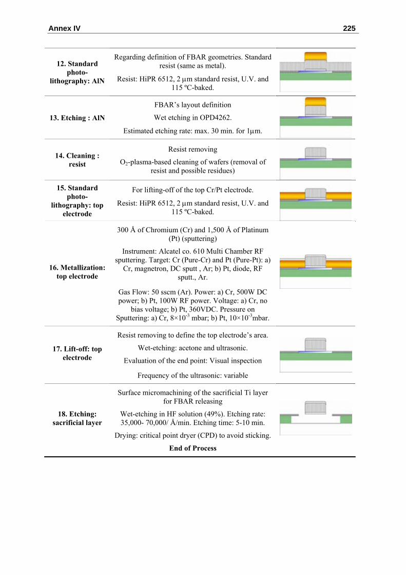
Annex IV 225
12. Standard photo-
lithography: AlN
Regarding definition of FBAR geometries. Standard resist (same as metal).
Resist: HiPR 6512, 2 μm standard resist, U.V. and 115 ºC-baked.
13. Etching : AlN
FBAR’s layout definition
Wet etching in OPD4262.
Estimated etching rate: max. 30 min. for 1μm.
14. Cleaning : resist
Resist removing
O2-plasma-based cleaning of wafers (removal of resist and possible residues)
15. Standard
photo-lithography: top
electrode
For lifting-off of the top Cr/Pt electrode.
Resist: HiPR 6512, 2 μm standard resist, U.V. and 115 ºC-baked.
16. Metallization: top electrode
300 Å of Chromium (Cr) and 1,500 Å of Platinum (Pt) (sputtering)
Instrument: Alcatel co. 610 Multi Chamber RF sputtering. Target: Cr (Pure-Cr) and Pt (Pure-Pt): a)
Cr, magnetron, DC sputt , Ar; b) Pt, diode, RF sputt., Ar.
Gas Flow: 50 sscm (Ar). Power: a) Cr, 500W DC power; b) Pt, 100W RF power. Voltage: a) Cr, no
bias voltage; b) Pt, 360VDC. Pressure on Sputtering: a) Cr, 8×10⁻³ mbar; b) Pt, 10×10-3mbar.
17. Lift-off: top electrode
Resist removing to define the top electrode’s area.
Wet-etching: acetone and ultrasonic.
Evaluation of the end point: Visual inspection
Frequency of the ultrasonic: variable
18. Etching: sacrificial layer
Surface micromachining of the sacrificial Ti layer for FBAR releasing
Wet-etching in HF solution (49%). Etching rate: 35,000- 70,000/ Å/min. Etching time: 5-10 min.
Drying: critical point dryer (CPD) to avoid sticking.
End of Process

Annex V
Back-side, bulk-micromachining process for FBAR fabrication
Step Purpose, instruments and conditions Layout
Wafer preparation and
cleaning
Wafers of thickness: 300μm +/- 15μm are implemented.
Preparation of P-wafers, with resistivity of 4-40 Ohm.cm
Standard cleaning of all wafers is performed (cascade and rinsing in track).
Cleaning material: Three-step process: a) H2SO4 + H2O2 (2:1) Cleansing, 10min.; b) De-ionized H2O, 5 min.; c) De-ionized H2O, 10 min. Temperature: 110
– 125 ºC
1. Oxidation
Thermal oxidation –SiO2– of silicon surface; 4,000 Å (front-side and back-side)
Instrument: ASM (oven)
Temperature: 1100 ºC. Time: Three-step: a) Dry, 10min; b) Wet, 1h:35min; c) Dry, 10min. Gas flow
(for previous steps): a) O2, 6.0 sccm; b) H2+O2, 5.0/3.5 sccm; c) O2, 6.0 sccm
2. Deposition : Si3N4
Buffer layer for back-side etching.
Standard deposition of 1,800 Å (back-side of the wafer)
Oven: T10
3. Standard photo-
lithography: Si3N4
For back-side etching of Si substrate.
Alignment and exposure: In CanonPLA600. Proximity mode 3- μm gap. Priming –coating- soft-
bake: HMDS vapor priming, time=25’’. Coating 1.2 μm of HiPR 6512. Soft-bake in hot-plate
T=100ºC. Contact time=20’’.

228 FBAR: fabrication, heterogeneous integration and sensor applications
4. Etching: Si3N4
Access to the SiO2 layer (according to FBAR’s membrane size. Si3N4 is a buffer-layer)
Etching of 1,800 Å of Si3N4
Plasma etching. Instrument: Alcatel GIR-160.
5. Resist removing
Back-side Si3N4 passivation-resist removing
From previous step, remaining resist is removed (acid solution)
Dry etching. Instrument: TEPLA (O2 plasma). Power: 500W. Pressure: 0.8 mbar. Flow (O2): 10%.
Time: 30-45 min.
6. Etching: SiO2
Elimination of the front-side (no mask) AND of the back-side thermal-SiO2 (etch-window mask) layers
Etching of 4,000 Å of thermal-SiO2. Front-side: all SiO2 removed. Back-side: only the exposed SiO2 is removed (non-protected by the Si3N4 buffer layer)
Plasma etching. Instrument: AC2/1
7. Deposition: SiO2
PECVD- SiO2 membrane (passivation layer for etch-stopping and FBAR support)
Deposition of 5,000 Å of PECVD- SiO2
Instrument: T12
8. Standard photo-
lithography : bottom electrode
For lifting-off of the bottom Ti/Pt electrode.
Resist: HiPR 6512, 2 μm standard resist, U.V. and 115 ºC-baked. Instrument:
Karl Sus MA-1
9. Metallization: bottom electrode
300 Å of Chromium (Cr) and 1,500 Å of Platinum (Pt) (sputtering)
Instrument: Alcatel co. 610 Multi Chamber RF sputtering. Target: Cr (Pure-Cr) and Pt (Pure-Pt): a)
Cr, magnetron, DC sputt , Ar; b) Pt, diode, RF sputt., Ar.
Gas Flow: 50 sscm (Ar). Power: a) Cr, 500W DC power; b) Pt, 100W RF power. Voltage: a) Cr, no
bias voltage; b) Pt, 360VDC. Pressure on Sputtering: a) Cr, 8×10⁻³ mbar; b) Pt, 10×10-3mbar.
10. Lift-off: bottom electrode
Resist removing to define the bottom electrode’s area.
Wet-etching: acetone and ultrasonic.
Evaluation of the end point: Visual inspection
Frequency of the ultrasonic: variable

Annex V 229
11. Deposition : AlN
Acoustic layer of FBAR (10,000 Ǻ)
RF Sputtering, with suggested parameters: Al target (99.5% Al, 0.5% Cu), 1 kW power, Ar/N2: 50%
each, 1×10⁻² mbar pressure at sputtering chamber. Estimated deposition rate: 6-7 nm/min.
12. Standard photo-
lithography: AlN
Regarding definition of FBAR geometries. Standard resist (same as metal).
Resist: HiPR 6512, 2 μm standard resist, U.V. and 115 ºC-baked.
13. Etching : AlN
FBAR’s layout definition
Wet etching in OPD4262.
Estimated etching rate: max. 30 min. for 1μm.
14. Cleaning : resist
Resist removing
O2-plasma-based cleaning of wafers (removal of resist and possible residues)
15. Standard
photo-lithography: top
electrode
For lifting-off of the top Cr/Pt electrode.
Resist: HiPR 6512, 2 μm standard resist, U.V. and 115 ºC-baked.
16. Metallization: top electrode
300 Å of Chromium (Cr) and 1,500 Å of Platinum (Pt) (sputtering)
Instrument: Alcatel co. 610 Multi Chamber RF sputtering. Target: Cr (Pure-Cr) and Pt (Pure-Pt): a)
Cr, magnetron, DC sputt , Ar; b) Pt, diode, RF sputt., Ar.
Gas Flow: 50 sscm (Ar). Power: a) Cr, 500W DC power; b) Pt, 100W RF power. Voltage: a) Cr, no
bias voltage; b) Pt, 360VDC. Pressure on Sputtering: a) Cr, 8×10⁻³ mbar; b) Pt, 10×10-3mbar.
17. Lift-off: top electrode
Resist removing to define the top electrode’s area.
Wet-etching: acetone and ultrasonic.
Evaluation of the end point: Visual inspection
Frequency of the ultrasonic: variable
18. Etching: Si substrate (back-
side)
Back-side bulk micromachining of the Si substrate for FBAR releasing.
Anisotropic, wet-etching of Si in KOH solution. Etching rate: 35,000- 70,000/ Å/min. Etching time:
5-10 min.
Drying: critical point dryer (CPD) to avoid sticking.
End of Process

230 FBAR: fabrication, heterogeneous integration and sensor applications

Annex VI
Instrumentation for device and material characterization
Instrument Reference-model Application
Nanospec Nanometrics Modelo : Nanospec AFT-200
Thin-film thickness measurement (ex. AlN)
Tencor Tencor - Alpha-Step Thin-film thickness measurement (ex. AlN)
AFM Nanoscope IV controller and Dimension 3100 head from Veeco
Thin-film roughness inspection (ex. AlN)
SEM SEM LEO 1530 microscope and
RAITH ELPHY PLUS controller and software
FBAR structural characterization and imaging
FIB
CrossBeam 1560XB de Carl Zeiss (CNM-ICN)
FEI DB Strata235 FIB, a dual beam instrument (UB)
Thermal oxide is implemented as passivation layer for Si. Deposited and TEOS are
structural layers of temperature-compensated FBARs.
XRD BRUKER-binary V2 (.RAW),
FWHM calculation using POWD-12++ (UB)
Crystallographic characterization of AlN
Interferometer Zygo-interferometer and microscope application
FBAR structural and low-frequency characterization
Confocal Microscope: Nikon – Eclipse L150
Software: PLU Imaging Profiler
FBAR structural characterization and micro-
machining process inspection
Optical microscopy Microscope Nikon Eclipse ME-600 and digital camera DXM1200F FBAR structural inspection
DC Probe Station Karl Süss – Süss Micro Tec Probe Shield PA200
Low-frequency characterization of FBAR

232 FBAR: fabrication, heterogeneous integration and sensor applications
I/V parameter analyzer Hewlett-Packard 4155B Semiconductor Parameter Analyzer
Short-circuit and open conditions evaluation in FBAR
electrodes
Capacitance meter Hewlett-Packard 4280A 1MHz C Meter / C-V Plotter
Parallel-plate FBAR’s capacitance C0 characterization
Microwave Probe Station and RF Calibration
Station Suss Microtec
Probes Infinity. Pitch 150um. Configuration GSGSG
Calibration Standards:
a) Probes: Cascade Impedance standard Substrate 126-102
b) Connectors: Agilent
S-parameter characterization of FBAR (low and high-
frequency)
Network Analyzer Agilent Technologies E5100A 100kHz – 6GHz
S-parameter characterization of FBAR (low and high-
frequency)
Prototyping
Prototyping
PCB substrate: Rogers 3010
Connectors: SMA 3.5mm
S-parameter characterization of FBAR (low and high-
frequency)
DC Power Supply Keithley 230 programmable voltage source DC-tuning of FBAR

Annex VII
List of Publications
Patents [P1] H. Campanella, J. Esteve, E. Cabruja, J. Montserrat, L. Terés, M. Carmona, “Thin-film bulk
acoustic wave resonator and method for performing heterogeneous integration of the same with complementary-metal-oxide-semiconductor integrated circuit”. European Patent Agency, Application No. EP07380041. 2007.
Journals [J1] H. Campanella, E. Cabruja, J. Montserrat, A. Uranga, N. Barniol, and J. Esteve, “Thin-film
bulk acoustic wave resonator floating above CMOS substrate”, IEEE Electron Device Letters 29 (2008) 28-30.
[J2] H. Campanella, P. Nouet, P. de Paco, A. Uranga, N. Barniol, and J. Esteve, “Automated on-wafer extraction of equivalent-circuit parameters in thin-film bulk acoustic wave resonators (FBAR) and substrate” in Microwave and Optical Technology Letters 50 (2008) 4-7.
[J3] H. Campanella, A. Uranga, A. Romano-Rodríguez, J. Montserrat, G. Abadal, N. Barniol, and J. Esteve, “Localized-mass detection based on thin-film bulk acoustic wave resonators (FBAR): area and mass location aspects”, Sensors Actuators A: Physical 142 (2008) 322-328.
[J4] H. Campanella, F. Hernández-Ramírez, A. Romano-Rodríguez, J. Montserrat, A. Uranga, N. Barniol, and J. Esteve, “Focused-ion-beam-assisted tuning of thin-film bulk acoustic wave resonators (FBAR)”, Journal of Micromechanics and Microengineering 17 (2007) 2380-2389.
[J5] H. Campanella, J. Esteve, J. Montserrat, A. Uranga, G. Abadal, N. Barniol, and A. Romano-Rodríguez, “Localized and distributed mass detectors with high sensitivity based on thin-film bulk acoustic resonators”, Applied Physics Letters, 89 (2006) 033507.
[J6] H. Campanella, J. Esteve, J. Montserrat, A. Uranga, G. Abadal, N. Barniol, and A. Romano-Rodríguez, “Possibilities of thin-film bulk acoustic resonators as punctual mass sensors”, Journal of the. Acoustical Society of America, 119 (2006) 3414.
[J7] H. Campanella, J. Esteve, J. Montserrat, A. Uranga, G. Abadal, N. Barniol, and A. Romano-Rodríguez, “Localized and distributed mass detectors with high sensitivity based on thin-film bulk acoustic resonators”, Virtual Journal of Biological Physics Research, 12 (2006) 3. Available on-line: http://www.vjbio.org

234 FBAR: fabrication, heterogeneous integration and sensor applications
Conference contributions (published in proceedings with referee committee) [C1] H. Campanella, J.A. Plaza, J. Montserrat, A. Uranga, N. Barniol, and J. Esteve,
“Accelerometer based on thin-film bulk acoustic wave resonators”. In Proc. IEEE International Ultrasonics Symposium 2007. New York, NY, USA, Oct. 28-31, 2007, 1148-1151. ISBN 978-1-4244-1384-3.
[C2] H. Campanella, J. A. Plaza, J. Montserrat, C. Mateu, A. Uranga, N. Barniol, and J. Esteve, “Micro-machining technology for the fabrication of embedded-FBAR accelerometer”. In Proc. 18th Workshop on Micro-Mechanics Europe MME 2007, Guimaraes, Portugal, Sep. 16-18, 2007, 43-46. ISBN 978-972-98603-3-1.
[C3] H. Campanella, J. Esteve, A. Uranga, P. De Paco, N. Barniol, and P. Nouet, “Instantaneous de-embedding of the on-wafer equivalent-circuit parameters of acoustic resonator (FBAR) for integrated circuit applications”. In Proc. 20th Symposium on Integrated Circuits and Systems Design SBCCI’07, Rio de Janeiro, Brazil, Sept. 3–6, 2007, 212-217. ISBN 978-1-59593-910-4.
[C4] H. Campanella, A. Uranga, P. Nouet, N. Barniol, L. Terés and J. Esteve. “Design and characterization of a bulk-acoustic-resonator (FBAR)”. In Proc. 8th Intl. Symposium on RF MEMS and RF Microsystems Memswave 2007, Barcelona, Spain, June 26-29 2007, 83-86. ISBN 978-84-96736-22-1.
[C5] H. Campanella, P. Nouet, P. de Paco, A. Uranga, N. Barniol, and J. Esteve. “Automated on-wafer characterization in micro-machined resonators: towards an integrated test vehicle for bulk acoustic wave resonators (FBAR)”. In Proc. IEEE Intl. Conf. Microelectronic Test Structures ICMTS 2007, Tokyo, Japan, March 19-22, 2007, 157-161. ISBN 1-4244-0780-X.
[C6] H. Campanella, J. Esteve, J. Montserrat, A. Romano-Rodríguez, A. Uranga, G. Abadal, and N. Barniol “Sensitivity considerations in localized mass detection based on thin-film bulk acoustic wave resonators”. In Proc. IEEE International Ultrasonics Symposium 2006, Vancouver, Canada, Oct. 3-6, 2006, 1828-1831. ISBN 1-4244-0202-6.
[C7] H. Campanella, J. Esteve, A. Romano-Rodríguez, J. Montserrat, A. Uranga, G. Abadal, and N. Barniol. “Punctual mass detection based on thin-film bulk acoustic wave resonators: area and mass location aspects”. In Proc. Eurosensors 2006, XX Anniversary. Goteborg, Sweden, Sep. 17-20, 2006, 72-73. ISBN 978-91-631-9280-7
[C8] H. Campanella, J. Esteve, J. Montserrat, A. Romano-Rodríguez, A. Uranga, and N. Barniol. “Process considerations in fabricating bulk acoustic wave resonators”. Micro and Nanotechnologies MNE 2006. Barcelona, Spain, Sep. 17-20, 2006.
[C9] H. Campanella, J. Esteve, A. Romano-Rodríguez, J. Montserrat, A. Uranga, and N. Barniol. “Focused-ion-beam-assisted tuning of thin-film bulk acoustic wave resonators”. In Proc. 17th Workshop on Micro-Mechanics Europe MME 2006. Southampton, UK. Sep. 3-5, 2006, 21-24. ISBN 085432 8483.
[C10] A. Uranga, N. Barniol, H. Campanella, J. Esteve, L. Terés, Z. Davis. “A Read-Out Strategy and Circuit Design for High Frequency MEMS Resonators”. In Proc. IEEE International Symposium on Circuits and Systems 2005 ISCAS 2005, Kobe, Japan, May 23-26, 2005, 5361-5364. ISBN 0-7803-8835-6.
[C11] H. Campanella, A. Uranga, Z. Davis, J. Esteve, L. Terés, N. Barniol. “Band-pass transimpedance read out circuit for UHF MEMS resonator applications”. In Proc. SPIE Symposium on Microtechnologies for the New Millennium 2005, Sevilla, Spain, May 9-11, 2005, Volume 5837, 300-309. ISBN 0-8194-5849-X.