![Manual Aplicacion[1]](https://static.fdocuments.ec/doc/165x107/5571fcda4979599169980f63/manual-aplicacion1.jpg)
Aplicacion Note UC3843 (1)
12
UC3843 Fixed Frequency Current Mode PWM Controller 1 Rev 1.0 Jun. 2008 DESCRIPTION FEATURES APPLICATION ORDERING INFORMATION Temperature Range Package Orderable Device Package Qty SOP8L Pb-Free UC3843D 75Units/Tube DIP8L PIN CONFIGURATION UC3843P 50Units/Tube UC3843 is a fixed frequency current-mode PWM controller. It is specially designed for Off Line and DC-to-DC converter applications with minimal external component. This integrated circuit features a trimmed oscillator for precise duty cycle control, a temperature compensa ted reference, a high gain error amplifier, a current sensing comparator, and a high current totem pole output ideally suited for driving a power MOSFET . The device is protective features consisting of input and reference under-voltag e lockouts each with hysteresis, cycle-by-cycle current limiting. 1 2 3 4 5 6 7 8 (Top View) Compensation Voltage Feedback Current Sense RT/CT Vref VCC Output GND ● Wireless Base Station Power ● Telecom and Datacom Power ● Industrial Power Systems ● PC Power Supplies ● Automatic Feed Forward Compensation ● High Current Totem Pole Output ● Internally Trimmed Bandgap Reference ● Undervoltage Lockout with Hysteresis ● Low Start Up Current ● Optimized for offli ne conve rter ● Double pulse suppression ● Current mode operation to 500kHz 0°C to +70°C
Transcript of Aplicacion Note UC3843 (1)

7/22/2019 Aplicacion Note UC3843 (1)
http://slidepdf.com/reader/full/aplicacion-note-uc3843-1 1/11
UC3843
Fixed Frequency Current Mode PWM Controller
1
Rev 1.0
Jun. 2008
DESCRIPTION
FEATURES
APPLICATION
ORDERING INFORMATION
Temperature Range PackageOrderable
DevicePackage Qty
SOP8LPb-Free
UC3843D 75Units/TubeDIP8L
PIN CONFIGURATION
UC3843P 50Units/Tube
UC3843 is a fixed frequency current-mode PWM controller.
It is specially designed for Off Line and DC-to-DC converter
applications with minimal external component. This
integrated circuit features a trimmed oscillator for precise
duty cycle control, a temperature compensated reference, a
high gain error amplifier, a current sensing comparator, and
a high current totem pole output ideally suited for driving a
power MOSFET.
The device is protective features consisting of input and
reference under-voltage lockouts each with hysteresis,
cycle-by-cycle current limiting.
1
2
3
4 5
6
7
8
(Top View)
Compensation
Voltage Feedback
Current Sense
RT/CT
Vref
VCC
Output
GND
Wireless Base Station Power
Telecom and Datacom Power
Industrial Power Systems
PC Power Supplies
Automatic Feed Forward Compensation
High Current Totem Pole Output
Internally Trimmed Bandgap Reference
Undervoltage Lockout with Hysteresis
Low Start Up Current
Optimized for offline converter
Double pulse suppression
Current mode operation to 500kHz
0°C to +70°C

7/22/2019 Aplicacion Note UC3843 (1)
http://slidepdf.com/reader/full/aplicacion-note-uc3843-1 2/11
UC3843
2
Rev 1.0
Jun. 2008
SCHEMATIC DIAGRAM
PIN DESCRIPTION
No. Name Function Description
1 CompensationThis pin is the Error Amplifier output and is made available for loop
compensation.
2Voltage
Feedback
This is the inverting input of the Error Amplifier. It is normally
connected to the switching power supply output through a resistor
divider.
3 Current Sense A voltage proportional to inductor current is connected to this inputThe PWM uses this information to terminate the output switch
conduction.
4 RT/CT
The Oscillator frequency and maximum Output duty cycle are
programmed by connecting resistor RT to VREF and capacitor CT to
ground. Operation to 500kHz is possible.
5 GND This pin is the combined control circuitry and power ground.
6 OutputThis output directly drives the gate of a power MOSFET.
Peakcurrents up to 1.0A are sourced and sunk by this pin.
7 VCC This pin is the positive supply of the control IC.
8 VREFThis is the reference output. It provides charging current for capacitor
CT through resistor RT
Figure 1. Simplified Block Diagram
+-
Vref
8(14)
RTCT
4(7)
Voltage
Feedback
Input2(3)
Output
Compensation1(1)
VCC 7(12)
VC
7(11)
Output
6(10)
Power
Ground
5(8)
Current
Sense
Input3(5)
GND 5(9)
Error
Amplifier
Oscillator
Latching
PWM
Vref
Undervoltage
Lockout
5.0V
Reference
VCC
Undervoltage
Lockout
Pin numbers in parenthesis are for the D suffix SOIC-14 package.
R
R

7/22/2019 Aplicacion Note UC3843 (1)
http://slidepdf.com/reader/full/aplicacion-note-uc3843-1 3/11
UC3843
3
Rev 1.0
Jun. 2008
ABSOLUTE MAXIMUM RATINGS
Symbol Value Unit
Total Power Supply and Zener Current ICC + IZ 30
DC Supply Voltage VCC 30 V
Output Current Io ±1.0 A
Output Energy (Capacitive Load per Cycle) W 5.0 µJ
Error Amp Output Sink Current Ioe 10 mA
Current Sense and Voltage Feedback Inputs VIN -0.3 to 5.5 V
Maximum Power Dissipation @T A=25°C PD 0.862 W
Thermal Resistance, Junction-to-Air RBIA 145 °C/W
Maximum Operating Junction Temperature TJ +150 °C
Storage Temperature Range TSTG -65 to +150
Parameter Symbol Min Max Unit
DC Supply Voltage VCC 12 25 V
mA
°C
Parameter
Operating Temperature T A 0 70 °C
ELECTRICAL CHARACTERISTICS(Vcc = 15V unless otherwise noted)
Parameter Symbol Test Conditions Min Max Unit
4.9 5.1
Reference Out VREF
4.865 5.135
V
Line Regulation RegLINE 20 mV
Load Regulation RegLOAD 25 mV
Total Output Variation
over Line, Load,
Temperature (Note1)
VFINAL 4.82 5.18 V
Output Short Circuit
Current ISC -30 -180 mA
RECOMMENDED OPERATION CONDITIONS
IO = 1.0mA, VCC = 15V,
T A = 25±10°C
IO = 1.0mA, VCC = 15V,
T A = TLOW to THIGH
VCC = 12V to 25V,
T A = TLOW to THIGH
IO = 1.0 to 20mA,
T A = TLOW to THIGH
VCC = 12V, IO = 1.0mA,
T A = TLOW to THIGH
VCC = 25V, IO = 20mA,
T A = TLOW to THIGH
VCC =15V
Reference Section

7/22/2019 Aplicacion Note UC3843 (1)
http://slidepdf.com/reader/full/aplicacion-note-uc3843-1 4/11
UC3843
4
Rev 1.0
Jun. 2008
VCC = 15V, TJ = 25°C
RT=10K
, CT = 3.3nF
47 57
Frequency f osc
VCC = 15V,
T A = TLOW to THIGH,
RT = 10KCT = 3.3nF
46 60
kHz
Frequency Change with Voltage
Δ f osc/ΔV 1.0 %
TJ = 25°C 7.5 9.3
Discharge Current IdischVosc = 2.0V
VCC = 15VT A = TLOW to
THIGH 7.2 9.5
mA
Error Amplifier Section
Voltage Feedback
InputVFB
VO = 2.5V,VCC = 15V,
T A = TLOW to THIGH2.42 2.58 V
Input Bias Current IIBVFB = 2.7V,VCC = 15V,
TA = TLOW to THIGH-2.0 µA
Open Loop Voltage
Gain AVOL
VO = 2.0V to 4.0V,
VCC = 15V,
T A = TLOW to THIGH
65 dB
Unity Gain Bandwidth BWVCC = 15V,
T A = TLOW to THIGH0.7 MHz
Power Supply
Rejection RatioPSRR
VCC = 12V to 25V,
T A = TLOW to THIGH
60 dB
Sink ISINK
VO = 1.1V, VFB = 2.7V,
VCC = 15V,
T A = TLOW to THIGH
2.0Output
Current
Source ISOURCE
VO = 5.0V, VFB = 2.3V,
VCC = 15V,T A = TLOW to THIGH
-0.5
mA
High
StateVOH 5.0
Output
Voltage
Swing Low
StateVOL
VFB = 2.7V, VCC = 15V
RL(5.0) = 15KΩ,
T A = TLOW to THIGH
1.1
V
Oscillator Section
VFB = 2.7V, VCC = 15V
RL(GND) = 15KΩ,
T A = TLOW to THIGH
ELECTRICAL CHARACTERISTICS
Parameter Symbol Test Conditions Min Max Unit
VCC = 12V to 25V,
T A= TLOWto THIGH,
RT=10kΩ, CT=3.3nF

7/22/2019 Aplicacion Note UC3843 (1)
http://slidepdf.com/reader/full/aplicacion-note-uc3843-1 5/11
UC3843
5
Rev 1.0
Jun. 2008
Output SectionISINK = 20mA, VCC = 15V 0.4Low
StateVOL
ISINK = 200mA, VCC = 15V 2.2
13
Output
Voltage High
StateVOH
12
V
Output Voltage with
UVLO ActivatedVOL(UVLO)
VCC = 6V, ISINK = 1.0mA,
T A = TLOW to THIGH1.1 V
tr CL = 1.0nF,VCC= 15V,
T A = TLOW to THIGH150 ns
Output Voltage Fall
Time tf 150 ns
Under Voltage Lockout Section
Startup Threshold Vth 7.8 7.9 V
Minimum Operating
Voltage After Turn-OnVCC(MIN) 7.0 8.2 V
PWM Section
Duty Cycle DC
VCC = 15V,
T A = TLOW to THIGH,
RT = 10KΩ, CT = 3.3nF
0 94 %
Total Device
Startup: VCC = 14V 1.0Power Supply Current ICC
Operating: VCC = 15V 17mA
Power Supply Zener
VoltageVz ICC = 25mA, VCC = 0 to 40V 30 40 V
Note 1: VFINAL = VREF25(RegLINE+RegLOAD)/1000±IVREF70(VREF0)-VREF25I VREF25 = VREF@T A=25°C;
VREF70=VREF@T A=70°C;VREF0=VREF@T A=0°C.
Note 2: TLOW = 0°C,THIGH=+70°C
ISINK = 20mA, VCC = 15V
ISINK = 200mA, VCC = 15V
VCC = 0V to 25V,
T A = TLOW to THIGH
Output Voltage
Rise Time
Current Sense Section
Current Sense Input
Voltage Gain AV
VFB = 0V, VCC = 15V,
T A = TLOW to THIGH 2.85 3.15
Maximum Current
Sense Input
Threshold
VTH 0.9 1.1 V
Input Bias Current IIB -10 µA
Propagation Delay
(Current Sense Input
to Output)
tPLH 300 ns
VFB = 0V,VCC = 15V,
T A = TLOW to THIGH
VCC = 15V,
T A = TLOW to THIGH
VCC = 15V,
T A = TLOW to THIGH
ELECTRICAL CHARACTERISTICS(CONTINUE)
Parameter Symbol Test Conditions Min Max Unit
CL = 1.0nF, VCC = 15V,
T A = TLOW to THIGH
VCC = 0V to 25V,
T A = TLOW to THIGH

7/22/2019 Aplicacion Note UC3843 (1)
http://slidepdf.com/reader/full/aplicacion-note-uc3843-1 6/11
UC3843
6
Rev 1.0
Jun. 2008
Figure 2. Timing Resistor versus
Oscillator Frequency
Figure 3. Output Deadtime versus
Oscillator Frequency
Figure 4. Oscillator Discharge Current
versus Temperature
Figure 5. Maximum Output Duty Cycle
versus Timing Resistor
Figure 6. Error Amp Small SignalTransient Response
Figure 7. Error Amp Large SignalTransient Response
VCC = 15V
VOSC = 20V
2.55V
2.5V
2.45V
2.5V
3.0V
2.0V
100
50
20
10
5.0
2.0
1.0
9.0
8.5
8.0
7.5
7.0
100
90
80
70
60
50
40
TYPICAL PERFORMANCE CHARACTERISTICS
f OSC,OSCILLATOR FREQUENCY (Hz)
VCC = 15V
T A = 25°C
80
50
20
8.0
5.0
2.0
0.8
R T ,
T I M I N G
R E S
I S T O R ( k Ω )
10K 20K 50K 100K 200K 500K 1.0M
% D
T , P
E R C E N T O U T P U
T D E A D R M E
10K 20K 50K 100K 200K 500K 1.0M
VCC = 15V
T A = 25°C
f OSC,OSCILLATOR FREQUENCY (Hz)
I d i s c h g ,
D I S C H A R G E C U R R E N T ( m A )
-55 -25 0 25 50 75 100 125T A, AMBIENT TEMPERATURE (°C)
D m a x ,
M A X I M U M O
U T P U T D U T Y C Y C L E ( % )
800 1.0k 2.0k 3.0k 4.0k 6.0k 8.0k
Idischg = 9.5 mA
Idischg = 7.2 mA
VCC = 15 VCT = 3.3 nF
T A = 25°C
RT, TIMING RESISTOR (Ω)
VCC = 15 V
AV = -1.0T A = 25°C
2 0 m V / D
I V
0.5 µs/DIV
VCC = 15 V AV = -1.0
T A = 25°C
2 0 m V / D
I V
0.1 µs/DIV

7/22/2019 Aplicacion Note UC3843 (1)
http://slidepdf.com/reader/full/aplicacion-note-uc3843-1 7/11
UC3843
7
Rev 1.0
Jun. 2008
TYPICAL PERFORMANCE CHARACTERISTICS(CONTINUE)
Figure 8. Error Amp Open Loop Gain and
Phase versus Frequency
Figure 9. Current Sense Input Threshold
versus Error Amp Output Voltage
Figure 10. Reference Voltage Change
versus Source Current
Figure 11. Reference Short Circuit Current
versus Temperature
Figure 12. Reference Load Regulation Figure 13. Reference Line Regulation ∆ V O , O U T P U T V O L T A G E C H A N G E ( 2 . 0 m
V / D I V )
2.0 ms/DIV 2.0 ms/DIV
VCC =12V to 25V
Iref , REFERENCE SOURCE CURRENT (mA)
VCC=15V
T A=-55°CT A =125°C
T A, AMBIENT TEMPERATURE (°C) I S C , R E F E R E N C E
S H O R T C I R C U I T C U R R E N T ( m A )
0 110
90
70
50
T A =25°C
Gain
Phase
0
30
60
90
120
150
180
0
20
40
60
80
100
0
0.2
0.4
0.6
0.8
1.0
1.2
VCC= 15V
T A= 25°C
T A= -55°C
-4.0
-8.0
-12
-16
-20
-24
T A = 25°C
∆ V O , O U T P U T V O L T A G E C H A N G E ( 2 . 0 m
V / D I V )
-20
10 100 1.0k 10k 100k 1.0M 10M
A V O L , O P E N
L O O P V O L T A G
E G A I N
( d B )
f, FREQUENCY (Hz)
VCC = 15 V
VO = 2.0 V to 4.0 VRL = 100 K
T A = 25°C
f , E X C E S S P H A S E ( D E
G R E E S )
V t h , C U R R E N T S E N S E I N P U T T H R E S H O L D
( V )
T A = 125°C
0 2.0 4.0 6.0 8.0
VO, ERROR AMP OUTPUT VOLTAGE (V)
∆ V r e f , R E F E R E N C E V O L T A G E C H A N G E ( m V )
0 20 40 60 80 100 120
VCC = 15 V
RL ≤ 0.1Ω
-55 -25 0 25 50 75 100 125
VCC = 15 V
IO = 1.0 mA to 20 mAT A = 25°C

7/22/2019 Aplicacion Note UC3843 (1)
http://slidepdf.com/reader/full/aplicacion-note-uc3843-1 8/11
UC3843
8
Rev 1.0
Jun. 2008
TYPICAL PERFORMANCE CHARACTERISTICS(CONTINUED)
Figure 14. Output Saturation Voltage
versus Load Current
Figure 15. Output Waveform
Figure 17. Supply Current versus Supply Voltage
50 ns/DIV
CL = 1.0nF
100 ns/DIV
VCC = 15V
CL = 15pF
I C C , S U
P P L Y C U R R E N T
, V O , O
U T P U T V O L T A G E
8006004002000
IO, OUTPUT LOAD CURRENT (mA)
V s a
t , O U T P U T S A T U R A T I O
N
V O L T A G E ( V )
VCC
TA = 25°C
T A =-55°C
GND
T A = 25°C
Source Saturation
(Load to Ground)
VCC = 15V
80 s Pulsed Load
120 Hz Rate
VCC, SUPPLY VOLTAGE(V)
I C C , S
U P P L Y C U R R E N T ( m A )
RT = 10K
CT = 3.3nF
VFB = 0V
ISense = 0V
90%
10%
0
1.0
2.0
3.0
0
25
20
15
10
5
0
Sink Saturation
(Load to VCC)
T A =-55°C
-2.0
-1.0
T A = 25°C
VCC = 15V
T A = 25°C
T A = 25°C
1 0 0 m
A / D I V
2 0 V / D I V
U C X 8 4 2 A
U C X 8 4 3 A
Figure 16. Output Cross Conduction

7/22/2019 Aplicacion Note UC3843 (1)
http://slidepdf.com/reader/full/aplicacion-note-uc3843-1 9/11
UC3843
9
Rev 1.0
Jun. 2008
TYPICAL APPLICATION
R1
5Ω 1W
117 VACVARO
VM 68
C1
250µF
250V
R2
56kΩ 2W
R4
4.7kΩ
R3
20kΩ
R5 150 kΩ
C14
100 pF
C50.01µF
R6
10 kΩ
C6
0.0022µF
UC3844
C2
100µF
25V
C3
22µF
R9
68Ω
3W
C4
47µF
25V NC
D2
1N3612
D3
1N3612
USD1120 C7
470pF
1kΩ
R8
R7
22Ω
R12
4.7kΩ
2W
C9
3300pF
600V
D4
1N3613
NP
T1D6
U9D946L1
N5 C10
4700µF
10V
C11
4700µF
10V
R13
20kΩ
Q1
UFN833
R10
0.55Ω
1W
N12
N12
D7
UF81002
D8
UES1002
C12
2200µF
16V
C13
2200µF
16V
C8
680pF
600V
D8
1N3613
R11
2.7kΩ
2W
+6V
COM
+12V
±12V COM
−12V72
1
8
4 5
3
6
7/22/2019 Aplicacion Note UC3843 (1)
http://slidepdf.com/reader/full/aplicacion-note-uc3843-1 10/11
UC3843
10
Rev 1.0
Jun. 2008
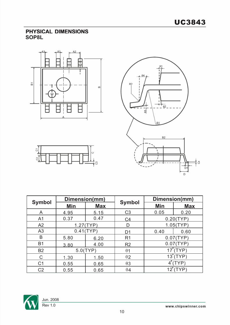
PHYSICAL DIMENSIONS
A
A1
A2
A3
B
B1
C
C1
C2
4.95 5.15
0.37 0.47
1.27(TYP)
0.41(TYP)
5.80 6.20
3.80 4.00
0.55
0.65
C4
D
D1
R1
R2
0.05 0.20
1.05(TYP)
0.20(TYP)
0.07(TYP)
13 (TYP)
4 (TYP)
12 (TYP)
1
2
3
4
B2
0.65
0.55
1.30 1.50
5.0(TYP)
C3
17 (TYP)
A2 A3
A
A1
B2
C 4
D1
R2
R1
C 1
C 2
C
C 3
D
0.40 0.60
0.07(TYP)
B
SOP8LPHYSICAL DIMENSIONS
Symbol Dimension(mm)
Min Max Symbol
Dimension(mm)
MaxMin
B 1
θ1
θ2
θ 3
θ4

7/22/2019 Aplicacion Note UC3843 (1)
http://slidepdf.com/reader/full/aplicacion-note-uc3843-1 11/11
UC3843
11
Rev 1.0
Jun. 2008
SymbolMin Max
A
A1
A2
A3
A4
A5
B
C
1.524(TYP)
0.39 0.53
2.54(TYP)
0.66(TYP)
0.99(TYP)
6.3 6.5
SymbolMin Max
C2
C4
D
D1
D2
8.20
0.20
7.62
5 (TYP)
8.80
0.35
7.87
Dimension(mm) Dimension(mm)
1
9.30 9.50
C1
7.20(TYP)
3.30 3.50
2
3
C3
0.5(TYP)
3.3(TYP)
8 (TYP)
8 (TYP)
1.57(TYP)
C 1
C 2
C 3
C 4
A1
A2
A3 A4
A5
D2
D1
A
B
C
D
DIP8L
θ1
θ2
θ3


![Esdep Lecture Note [Wg15a].1](https://static.fdocuments.ec/doc/165x107/577cc5801a28aba7119c99f5/esdep-lecture-note-wg15a1.jpg)