TEMARIO DEL CURSO DE FUNDAMENTOS DE FÍSICA DE …yolotli.inaoep.mx/portalfiles/diodoparte2.pdf ·...
28
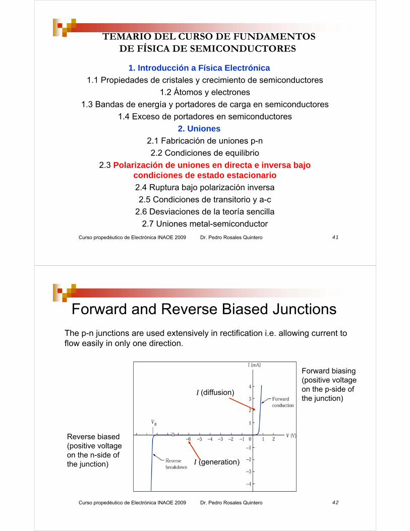
Curso propedéutico de Electrónica INAOE 2009 Dr. Pedro Rosales Quintero 41 1. Introducción a Física Electrónica 1.1 Propiedades de cristales y crecimiento de semiconductores 1.2 Átomos y electrones 1.3 Bandas de energía y portadores de carga en semiconductores 1.4 Exceso de portadores en semiconductores 2. Uniones 2.1 Fabricación de uniones p-n 2.2 Condiciones de equilibrio 2.3 Polarización de uniones en directa e inversa bajo condiciones de estado estacionario 2.4 Ruptura bajo polarización inversa 2.5 Condiciones de transitorio y a-c 2.6 Desviaciones de la teoría sencilla 2.7 Uniones metal-semiconductor TEMARIO DEL CURSO DE FUNDAMENTOS DE FÍSICA DE SEMICONDUCTORES Curso propedéutico de Electrónica INAOE 2009 Dr. Pedro Rosales Quintero 42 Forward and Reverse Biased Junctions The p-n junctions are used extensively in rectification i.e. allowing current to flow easily in only one direction. Forward biasing (positive voltage on the p-side of the junction) Reverse biased (positive voltage on the n-side of the junction) I (generation) I (diffusion)
-
Upload
vuongkhanh -
Category
Documents
-
view
232 -
download
7
Transcript of TEMARIO DEL CURSO DE FUNDAMENTOS DE FÍSICA DE …yolotli.inaoep.mx/portalfiles/diodoparte2.pdf ·...
Curso propedéutico de Electrónica INAOE 2009 Dr. Pedro Rosales Quintero 41
1. Introducción a Física Electrónica
1.1 Propiedades de cristales y crecimiento de semiconductores
1.2 Átomos y electrones
1.3 Bandas de energía y portadores de carga en semiconductores
1.4 Exceso de portadores en semiconductores
2. Uniones
2.1 Fabricación de uniones p-n
2.2 Condiciones de equilibrio
2.3 Polarización de uniones en directa e inversa bajo condiciones de estado estacionario
2.4 Ruptura bajo polarización inversa
2.5 Condiciones de transitorio y a-c
2.6 Desviaciones de la teoría sencilla
2.7 Uniones metal-semiconductor
TEMARIO DEL CURSO DE FUNDAMENTOS DE FÍSICA DE SEMICONDUCTORES
Curso propedéutico de Electrónica INAOE 2009 Dr. Pedro Rosales Quintero 42
Forward and Reverse Biased Junctions
The p-n junctions are used extensively in rectification i.e. allowing current to flow easily in only one direction.
Forward biasing(positive voltage on the p-side of the junction)
Reverse biased(positive voltage on the n-side of the junction) I (generation)
I (diffusion)

Curso propedéutico de Electrónica INAOE 2009 Dr. Pedro Rosales Quintero 43
Ideal model
The ideal diode: (a) diode circuit symbol; (b) i-v characteristic; (c) equivalent circuit in the reverse direction; (d) equivalent circuit in the forward direction.
Curso propedéutico de Electrónica INAOE 2009 Dr. Pedro Rosales Quintero 44
We assume that an applied voltage bias Vappears across the transition region (space charge region) of the junction rather than in the neutral n and p regions.¿?
Since an applied voltage changes the electrostatic potential barrier and thus the electric field within the transition region, we would expect changes in the various components of current at the junction.
Qualitative description of Current Flow at a Junction

Curso propedéutico de Electrónica INAOE 2009 Dr. Pedro Rosales Quintero 45
Thermal equilibrium
The current at V=0 (equilibrium) is zero since the generation (drift) and diffusion currents cancel.
p
EC
EV
EF
n
qVo
-xp0 xn0
( ) 0)( =−= driftIdiffusionII
-
-
+
diffusion
diffusion+ drift
drift
Curso propedéutico de Electrónica INAOE 2009 Dr. Pedro Rosales Quintero 46
Forward bias
p
EC
EV
EFn
The total electrostatic potential across the junction decreases by VF
nIF
+ -
q(V0-VF)
VF
Width of the depletion region decreases.
qVF
-xp xn
EFp
-
-
+
diffusion
diffusion+ drift
drift

Curso propedéutico de Electrónica INAOE 2009 Dr. Pedro Rosales Quintero 47
The total current I is the diffusion current minus the absolute value of generation current, which we will now refer to as I0:
⎟⎟⎠
⎞⎜⎜⎝
⎛−⎥
⎦
⎤⎢⎣
⎡=⎟⎟
⎠
⎞⎜⎜⎝
⎛−⎥⎦
⎤⎢⎣⎡= 1exp1exp 00
thv
VI
kT
qVII
⎟⎟⎠
⎞⎜⎜⎝
⎛⎥⎦⎤
⎢⎣⎡=
kT
qVII exp0
When V is positive and greater than a few kT/q (V>>3Vth), the exponential term is greater than the unity:
0II −=
When V is negative , the exponential term approaches to zero:
This negative generation current is also called the reverse saturation current
Curso propedéutico de Electrónica INAOE 2009 Dr. Pedro Rosales Quintero 48
We expect the minority carrier concentration on each side of the junction vary with the applied bias because of variations in the diffusion of carrier across the junction. The equilibrium ratio of holes concentrations on each side
[ ]kTqVp
p
n
p0exp=
Then under bias V, ( )( ) ( )[ ]kTVVqxp
xp
n
p −=−
00
0 exp
Carrier Injection
If we assume low-level injection of mobile carriers, that is the majority carrier densities are essentially unchanged under bias,
So taking the ratio of the previous two equations we get,
( ) pp pxp =− 0
( ) [ ]kTqVp
xp
n
n exp0 =

Curso propedéutico de Electrónica INAOE 2009 Dr. Pedro Rosales Quintero 49
As we can see, the minority carrier concentrations at the edge of the transition region are raised by the forward bias, The excess holes injected across the depletion region into the n side is given by,
( ) [ ]( )1exp0 −=−=∆ kTqVppxpp nnnn
Similarity for excess electrons injected on the p side
( ) [ ]( )1exp0 −=−−=∆ kTqVnnxnn pppp
Curso propedéutico de Electrónica INAOE 2009 Dr. Pedro Rosales Quintero 50
ppp
pp
DL
L
p
x
pp
x
pD
t
p
p
τ
δδτδδδ
=
=−∂∂
=−∂∂
=∂∂
;022
2
2
2
Boundary conditions are,
( ) ( ) ( ) nnn pxpandppxp =∞→∆=== δδ 00
Solution of δp(x) is,
( )⎥⎥⎦
⎤
⎢⎢⎣
⎡
⎥⎥⎦
⎤
⎢⎢⎣
⎡−⎥
⎦
⎤⎢⎣
⎡−⎟⎠⎞
⎜⎝⎛=
⎥⎥⎦
⎤
⎢⎢⎣
⎡−∆=
p
nn
p
nn L
x
kT
qVp
L
xpxp exp1expexpδ
Minority carrier density decays with a characteristic length given by Lp
From the continuity equation in the n region

Curso propedéutico de Electrónica INAOE 2009 Dr. Pedro Rosales Quintero 51
nnn
nn
DL
L
n
x
nn
x
nD
t
n
n
τ
δδτδδδ
=
=−∂∂
=−∂∂
=∂∂
;022
2
2
2
Boundary conditions are,
( ) ( ) ( ) ppp nxnandnnxn =∞→∆=== δδ 00
Solution of δn(x) is,
( ) ⎥⎦
⎤⎢⎣
⎡⎥⎦
⎤⎢⎣
⎡−⎥
⎦
⎤⎢⎣
⎡−⎟
⎠⎞
⎜⎝⎛=⎥
⎦
⎤⎢⎣
⎡−∆=
n
pp
n
pn L
x
kT
qVn
L
xpxn exp1expexpδ
Minority carrier density decays with a characteristic length given by Ln
From the continuity equation in the p region we can get:
Curso propedéutico de Electrónica INAOE 2009 Dr. Pedro Rosales Quintero 52
Current flowSince we assume that the drift current is unaffected by the applied bias, we are now in a position to consider the net current by considering only the diffusion of injected holes into n side,
( ) ( )( ) ( )( )xpL
DqA
dx
xpdqADxI
p
p
npnp δδ
=−=
Where A is the cross sectional area of the junction. The total hole current injected into the n-side is proportional to the excess hole density at a particular point. The total current injected into the n-side can be obtained by evaluating the previous equa. at x=xn0,
( ) ⎟⎟⎠
⎞⎜⎜⎝
⎛−⎥⎦
⎤⎢⎣⎡== 1exp0
kT
qVp
L
ADqXI n
p
pnp

Curso propedéutico de Electrónica INAOE 2009 Dr. Pedro Rosales Quintero 53
By similar analysis, the injection of the electrons in the p side leads to an electron current at the junction
( ) ⎟⎟⎠
⎞⎜⎜⎝
⎛−⎥⎦
⎤⎢⎣⎡−== 1exp0
kT
qVn
L
ADqXI p
n
npn
( ) ( )pnnp xIxII −+=
⎥⎥⎦
⎤
⎢⎢⎣
⎡+=
n
pn
p
nps L
nD
L
pDqAI 00
( )1−= kTeVs eII
Saturation current density
So, the total current into the diode is given by:
Curso propedéutico de Electrónica INAOE 2009 Dr. Pedro Rosales Quintero 54
There is another way to calculating the total current into a diode. This is called charge control approximation.

Curso propedéutico de Electrónica INAOE 2009 Dr. Pedro Rosales Quintero 55
0II −=
When V is negative, the exponential term approaches to zero:
This means that I0 is constant, but this is the ideal case.
Curso propedéutico de Electrónica INAOE 2009 Dr. Pedro Rosales Quintero 56
1. Introducción a Física Electrónica
1.1 Propiedades de cristales y crecimiento de semiconductores
1.2 Átomos y electrones
1.3 Bandas de energía y portadores de carga en semiconductores
1.4 Exceso de portadores en semiconductores
2. Uniones
2.1 Fabricación de uniones p-n
2.2 Condiciones de equilibrio
2.3 Polarización de uniones en directa e inversa bajo condiciones de estado estacionario
2.4 Ruptura bajo polarización inversa
2.5 Condiciones de transitorio y a-c
2.6 Desviaciones de la teoría sencilla
2.7 Uniones metal-semiconductor
TEMARIO DEL CURSO DE FUNDAMENTOS DE FÍSICA DE SEMICONDUCTORES

Curso propedéutico de Electrónica INAOE 2009 Dr. Pedro Rosales Quintero 57
Reverse Bias BreakdownWhen a sufficiently large reverse bias is applied to a p-n junction, it breaks down and conducts a very large current. There are 2 mechanisms by which this can occur…
The tunneling effect
This is the basis for the tunnel diode and one mechanism for storing and erasing charges in non-volatile semiconductor memory (NVSM) devices
Avalanche multiplication
This effect imposes an upper limit on the reverse bias in most devices. It limits the collector voltage of a bipolar transistor and the drain voltage of a MOSFET.
Curso propedéutico de Electrónica INAOE 2009 Dr. Pedro Rosales Quintero 58
The Tunnelling Effect
When a high electric field is applied to a p-n junction in the reverse direction, an electron can tunnel through the bandgap from the valence band to the conduction band.
EFn
EFp
<4Eg
EC
EV
EC
EV
E
Tunneling is the main breakdown mechanism for Si and GaAs junctions where the breakdown voltage is less than 4Eg/q
The tunnelling of electrons from the p side valence band to n side conduction band constitutes a reverse current from n to p, this is called Zener effect.

Curso propedéutico de Electrónica INAOE 2009 Dr. Pedro Rosales Quintero 59
Avalanche multiplication
Junction breakdown at reverse biases in excess of 6Eg / q is dominated by
avalanche multiplication…
EFn
EFp
>6Eg
EC
EV
EC
EV
EA thermally generated electrons in the depletion region gains kinetic energy from the electric field
On collision with a lattice atom it breaks the bond and generates an electron-hole pair
These in turn acquire kinetic energy from the electric field and generate more electron-hole
pairs…and so it continues.
Curso propedéutico de Electrónica INAOE 2009 Dr. Pedro Rosales Quintero 60
Critical field at breakdown versus background doping for Si and GaAs one-sided abrupt junctions.

Curso propedéutico de Electrónica INAOE 2009 Dr. Pedro Rosales Quintero 61
Curso propedéutico de Electrónica INAOE 2009 Dr. Pedro Rosales Quintero 62
1. Introducción a Física Electrónica
1.1 Propiedades de cristales y crecimiento de semiconductores
1.2 Átomos y electrones
1.3 Bandas de energía y portadores de carga en semiconductores
1.4 Exceso de portadores en semiconductores
2. Uniones
2.1 Fabricación de uniones p-n
2.2 Condiciones de equilibrio
2.3 Polarización de uniones en directa e inversa bajo condiciones de estado estacionario
2.4 Ruptura bajo polarización inversa
2.5 Condiciones de transitorio y a-c
2.6 Desviaciones de la teoría sencilla
2.7 Uniones metal-semiconductor
TEMARIO DEL CURSO DE FUNDAMENTOS DE FÍSICA DE SEMICONDUCTORES

Curso propedéutico de Electrónica INAOE 2009 Dr. Pedro Rosales Quintero 63
Transient and a-c ConditionsWe have considered the properties of p-n junctions under equilibrium and with steady state current. Most of the basics concepts of junction devices can be obtained from these properties, except for the important behavior of junctions under transient or ac conditions.
Since the most solid state devices are used for switching or for processing a-c signals.
We investigate the important influence of excess carries in transient and ac problems, i.e. the switching of a diode from its forward state to its reverse state is analyzed to illustrate a typical transient problem
Curso propedéutico de Electrónica INAOE 2009 Dr. Pedro Rosales Quintero 64
Time Variation of Stored ChargeFor a proper solution of the transient problem, we must to use the time dependent continuity equations. We can obtain each component of the current at position xand time t from these equations, we can write:
To obtain the instantaneous density current, we can integrate both sides at time t to obtain:
For injection into a long n region from a p+ region, we can take the current at xn=0 to be all hole current, and Jp at xn=∞ to be zero. Then the total injected current, including time variations, is
t
txpq
txpq
x
txJ
p
p
∂∂
+=∂
∂−
),(),(),(
τδ
dxt
txpq
txpqxJJ
x
ppp ∫
⎥⎥⎦
⎤
⎢⎢⎣
⎡
∂∂
+=−0
),(),()()0(
τδ
nnnnp
np dxtxpt
qAdxtxpqA
txiti ∫∫∞∞
∂∂
+===00
),(),(),0()( δτ

Curso propedéutico de Electrónica INAOE 2009 Dr. Pedro Rosales Quintero 65
dt
tdQtQti p
p
p )()()( +=
τThis results indicates that the hole current injected across the p+njunction is determined by two charge storage effects:
1. The usual recombination term in which the excess carrier distribution is replaced every τp seconds.
2. A charge buildup( or depletion )term.
We can solve for the stored charge as a function of time for a given current transient. For example the step turn–off transient.
Curso propedéutico de Electrónica INAOE 2009 Dr. Pedro Rosales Quintero 66
⎥⎥⎦
⎤
⎢⎢⎣
⎡−=
+=
−+=
ppp
p
pp
ppp
p
tItQ
s
ISQ
ISSQSQ
ττ
τ
τ
ττ
exp)(
1)(
)()(
0
Solving the previous equation with Laplace transforms, with i(t > 0) = 0 and Qp(0)=Iτp , we obtain
As expected, the stored charge dies out exponentially from its initial value Iτpwith a time constant equal to the hole lifetime in the n material

Curso propedéutico de Electrónica INAOE 2009 Dr. Pedro Rosales Quintero 67
The previous analysis does indicate clearly that the voltage across a p-n junction cannot be changed instantaneously, and that stored charge can present a problem in a diode intended for switch application.
Thus in the quasi-steady state approximation, the junction voltage varies according to
The switching process can be made still faster by purposely adding recombination centers, such as Au atoms in Silicon, to increase the recombination rate
⎥⎥⎦
⎤
⎢⎢⎣
⎡+⎟⎟⎠
⎞⎜⎜⎝
⎛−= 1expln)(
pnp
p t
pqAL
I
q
kTtv
ττ
Curso propedéutico de Electrónica INAOE 2009 Dr. Pedro Rosales Quintero 68
Reverse Recovery Transient
In most switching applications a diode is switched from forward conduction to reverse biased state. The resulting stored charge transient is somewhat more complicated than for a simple turn-off transient.
Lets us to assume a p+-n junction is driven by a square wave generator that periodically switches from +E to –E. While E is positive the diode is forward biased, and in steady state the current If flows through the junction. If E is much larger than the small forward voltage of the junction, the source voltage appears almost entirely across de resistor (R), the positive i = If ≈ E/R. After the voltage generator is reversed (t > 0), the current must be initially reverse to i = Ir≈ -E/R.

Curso propedéutico de Electrónica INAOE 2009 Dr. Pedro Rosales Quintero 69
The reason for this unusually large reverse current through the diode is that the stored charge.
The time (tsd) required for the stored charge to became zero is called the storage delay time. The critical parameter determining tsd is the carrier timelife (τp)
2
1
⎥⎥⎦
⎤
⎢⎢⎣
⎡⎟⎟⎠
⎞⎜⎜⎝
⎛
+= −
rf
fpsd II
Ierft τ
Curso propedéutico de Electrónica INAOE 2009 Dr. Pedro Rosales Quintero 70
Capacitance of p-n junctionsThere are two types of capacitance associated with a junction:
1. The junction capacitance due to dipole in the transition region. (depletion capacitance).
2. The charge storage capacitance arising from the lagging behind of voltage as current changes. (Diffusion capacitance).
The junction depletion layer capacitance per unit area is defined as Cj=dQ/dV, where dQ is the incremental change in the depletion layer charge per unit area for an incremental change in the applied voltage dV. The depletion capacitance per unit area is given by [ ]2/ cmF
WdQW
dQ
dV
dQCj s
s
ε
ε
===

Curso propedéutico de Electrónica INAOE 2009 Dr. Pedro Rosales Quintero 71
Thermal equilibrium
p
EC
EV
EF
What happens when we apply and external reverse bias across the junction?
n
qV0
-Wp Wn
Curso propedéutico de Electrónica INAOE 2009 Dr. Pedro Rosales Quintero 72
Reverse bias
p
EC
EV
EF
The total electrostatic potential across the junction increases by VR
nIR
- +
q(V0+VR)
VR
qVR
-Wp Wn
EFn
EFp

Curso propedéutico de Electrónica INAOE 2009 Dr. Pedro Rosales Quintero 73
Then, the width of the depletion region increases.
The depletion capacitance per unit area is the same as the standard expression for a parallel plate capacitor where the spacing between of the two plates represents the depletion layer width. In the case for a one-side abrupt junction (p+-n), we obtain
The quantity Cj is a voltage-variable capacitance, since Cjis proportional to (V0-V)1/2. The p-n junction device which makes use of the voltage variable properties of Cj is called a varactor.
[ ]VV
Nq
WCj dss
−==
02
εε
[ ]⎟⎟⎠
⎞⎜⎜⎝
⎛ +−=
da
das
NN
NN
q
VVW 02ε
Curso propedéutico de Electrónica INAOE 2009 Dr. Pedro Rosales Quintero 74
The diffusion capacitanceAs a p-n diode is forward biased, the minority carrier distribution in the quasi-neutral region increases dramatically. In addition, to preserve quasi-neutrality, the majority carrier density increases by the same amount. This effect leads to an additional capacitance called the diffusion capacitance. The excess minority-carrier charge is obtained by integrating the charge density over the quasi-neutral region. In the case of a p+ - n junction :
[ ]
p
th
pond
pd
Wn
Xn
nnp
IkT
q
Vth
V
V
nAqLC
dV
QdC
dxppeAQ
τ=
⎥⎦⎤
⎢⎣⎡==
∆=
−=∆ ∫
exp
0
Curso propedéutico de Electrónica INAOE 2009 Dr. Pedro Rosales Quintero 75
1. Introducción a Física Electrónica
1.1 Propiedades de cristales y crecimiento de semiconductores
1.2 Átomos y electrones
1.3 Bandas de energía y portadores de carga en semiconductores
1.4 Exceso de portadores en semiconductores
2. Uniones
2.1 Fabricación de uniones p-n
2.2 Condiciones de equilibrio
2.3 Polarización de uniones en directa e inversa bajo condiciones de estado estacionario
2.4 Ruptura bajo polarización inversa
2.5 Condiciones de transitorio y a-c
2.6 Desviaciones de la teoría sencilla
2.7 Uniones metal-semiconductor
TEMARIO DEL CURSO DE FUNDAMENTOS DE FÍSICA DE SEMICONDUCTORES
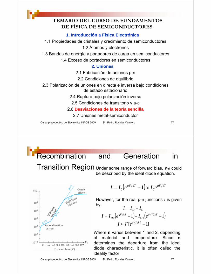
Curso propedéutico de Electrónica INAOE 2009 Dr. Pedro Rosales Quintero 76
Under some range of forward bias, We could be described by the ideal diode equation.
However, for the real p-n junctions I is given by:
Recombination and Generation in
Transition Region
( ) kTqVkTqV eIeII 00 1 ≈−=
( ) ( )]1´[
11 200
−≈
−+−=
+=
kTqV
kTqVG
kTqVD
GD
eII
eIeII
III
η
Where n varies between 1 and 2, depending of material and temperature. Since n determines the departure from the ideal diode characteristic, it is often called the ideality factor

Curso propedéutico de Electrónica INAOE 2009 Dr. Pedro Rosales Quintero 77
Reverse Bias Current Density
Under reverse bias (V is negative), the current goes towards the saturation current density (I0). As we can see from the ideal diode equation:
However, for Silicon and GaAs p-n junctions under reverse bias IR
≠ I0 !, and IR >> I0 ! Then, ???
( )10 −= kTqVeII
Curso propedéutico de Electrónica INAOE 2009 Dr. Pedro Rosales Quintero 78
Reverse Bias Generation Current Density
Under reverse bias, the generation current (IG) becomes to be very important when the depletion region is devoid of carries. Under thermal equilibrium the thermal generation of e-h pairs is balanced by recombination (G = R). Under reverse bias, there are very few e-h pairs in the depletion region, and the recombination rate is nearly zero. However, the thermal generation processes continuously supply the e-h pairs to depletion region. The IG can be determined from:
Then, IR = IG + I0 , and IG > I0 for Silicon and GaAs p-n
junctions under reverse bias
g
iW
g
iW
G
WqAndx
qAndxqAGI
ττ 2200
=== ∫∫

Curso propedéutico de Electrónica INAOE 2009 Dr. Pedro Rosales Quintero 79
Curso propedéutico de Electrónica INAOE 2009 Dr. Pedro Rosales Quintero 80
For higher forward bias voltages, the current no longer increases
exponentially with voltage. Instead, it increases linearly due to the
series resistance of the diode. This series resistance can be due to the
contact resistance between the metal and the semiconductor, due to the
resistivity of the semiconductor or due to the series resistance of the
connecting wires.
[ ])()( IRIRIVaV np +−=
I
+ V
-
+ Vj
-
RS
ID
- VR +
Ohmic Losses

Curso propedéutico de Electrónica INAOE 2009 Dr. Pedro Rosales Quintero 81
Small signal equivalent circuitof a p-n junction
V’d
Id
-I 0 V’+∆ Vd d
Vd
I’d
I’+∆ Id d
gd
V+ _d
Id
gd
Rs
Cd
thd nV/'V
thd
dd e
nV
I
V
Ig 0
opd
d==ddd V'VV ∆+=
Curso propedéutico de Electrónica INAOE 2009 Dr. Pedro Rosales Quintero 82
Graded junctionsThe case of linearity graded junction is shown in the next figure.

Curso propedéutico de Electrónica INAOE 2009 Dr. Pedro Rosales Quintero 83
The Poisson equation for the case is
222
2 Wx
Wax
q
dx
dE
dx
d
ss
s ≤≤−−=−=−=εε
ρψ
Where G is the impurity gradient (in cm -4) and W is the depletion–layer width. We obtain the built-in potential (Vbi) and the depletion layer width (W ) after some “simple steps”.
sbi
qaWV
ε12
2
=
3
1
12⎥⎦
⎤⎢⎣
⎡=
qa
VW bisε
Curso propedéutico de Electrónica INAOE 2009 Dr. Pedro Rosales Quintero 84
1. Introducción a Física Electrónica
1.1 Propiedades de cristales y crecimiento de semiconductores
1.2 Átomos y electrones
1.3 Bandas de energía y portadores de carga en semiconductores
1.4 Exceso de portadores en semiconductores
2. Uniones
2.1 Fabricación de uniones p-n
2.2 Condiciones de equilibrio
2.3 Polarización de uniones en directa e inversa bajo condiciones de estado estacionario
2.4 Ruptura bajo polarización inversa
2.5 Condiciones de transitorio y a-c
2.6 Desviaciones de la teoría sencilla
2.7 Uniones metal-semiconductor
TEMARIO DEL CURSO DE FUNDAMENTOS DE FÍSICA DE SEMICONDUCTORES

Curso propedéutico de Electrónica INAOE 2009 Dr. Pedro Rosales Quintero 85
Metal-Semiconductor Junction (Schottky barrier)
Metal n-Semiconductor
EV
EF
EC
Vacuum level
mqφ
( )χφ −mq
χqsqφ
What happens when we contact the metal and semiconductor in thermal equilibrium?
Curso propedéutico de Electrónica INAOE 2009 Dr. Pedro Rosales Quintero 86
Metal n-Semiconductor
EV
EF
EC
Vacuum level
The Fermi level must be constant at thermal equilibrium but the vacuum level must be continuous...
mqφ
Bnqφ
χq
sqφ0qV
Curso propedéutico de Electrónica INAOE 2009 Dr. Pedro Rosales Quintero 87
metal-semiconductor junction(Schottky barrier)
To ensure the continuity of the vacuum level, the Fermi level must move deeper into the semiconductor bandgap at the interface.
This involves electrons moving out from the semiconductor into the metal (which has so many electrons already that its Fermi level or band profile is unaffected).
As electrons move out, they leave behind uncompensated ionised donor atoms (as in a p++-n junction) and a depletion region is formed.
χφφ qqq mBn −=
The Schottky barrier height at the junction is the difference between the semiconductor conduction band and the metal Fermi level so that,
Curso propedéutico de Electrónica INAOE 2009 Dr. Pedro Rosales Quintero 88
Electrons moving from the semiconductor to the metal encounter an energy barrier given by the built-in potential,
smbi qqqV φφ −=
For the junction between a metal and a p-type semiconductor the barrier height and built in voltage are given by,
( )χφφ qqEq mgBp −−=
Sketch the band diagram to satisfy yourself that this is the case
msbi qqqV φφ −=

Curso propedéutico de Electrónica INAOE 2009 Dr. Pedro Rosales Quintero 89
Depletion width
Once the Schottky barrier height is known we can calculate the electric field profile, depletion width etc.
( )D
s
qN
VVW
−= 02ε
The problem for a Schottky barrier on an n-type semiconductor is identical to that for a one-sided abrupt p+-n junction (no depletion width on the metal side)…
ND is the donor concentration
V is the applied bias (positive forward, negative reverse)
Curso propedéutico de Electrónica INAOE 2009 Dr. Pedro Rosales Quintero 90
Metal-Semiconductor Junction Under Bias
EV
EF
ECBnqφ biqV
EV
EF
ECBnqφ( )VVq −0
EV
EF
ECBnqφ ( )VVq −0
Zero bias
Forward bias (V is positive)Decreased barrier to electrons flow from the semiconductor to the metal
Reverse bias (V is negative)Increased barrier to electrons flow from the semiconductor to the metal …rectification

Curso propedéutico de Electrónica INAOE 2009 Dr. Pedro Rosales Quintero 91
Figure 7.7. Current transport by the thermionic emission process. (a) Thermal equilibrium; (b) forward bias; and (c) reverse bias.
Current flow in a Schottky barrier
Curso propedéutico de Electrónica INAOE 2009 Dr. Pedro Rosales Quintero 92
Current flow in a Schottky barrier
At thermal equilibrium the flow of electrons from the semiconductor to the metal is exactly balanced by the flow of electrons from the metal to the semiconductor so,
Since the barrier height on the metal side is not dependent on the applied bias the current from metal to semiconductor will always be the same so the net current under bias is then,
kTqCmssm
BneCNJJ φ−→→ ==
( )1−=−= −→→
kTqVkTqCsmms eeCNJJJ Bnφ
Saturation current density, Js
( )1−= kTqVs eJJ
…rectification

Curso propedéutico de Electrónica INAOE 2009 Dr. Pedro Rosales Quintero 93
2exp* kTkT
AJ BS ⎥⎦
⎤⎢⎣⎡−=
φ
Thermionic Field Emission( )[ ][ ] ( ) ( )( )
⎥⎦
⎤⎢⎣
⎡ −−−
−−
⎥⎦⎤
⎢⎣⎡
−−−=
000
21
00 expcosh
*
E
EEq
kT
EEq
kT
Ek
EEVqETAJ fnCBfnCfnCB
S
φφπ
⎥⎦
⎤⎢⎣
⎡−=
000 exp
E
qJstJ B
S
φ
TFE
FE
TE
Thermionic Emission
Field Emission
Transport Mechanisms in Schottkydiodes
Curso propedéutico de Electrónica INAOE 2009 Dr. Pedro Rosales Quintero 94
Typical Schottky Barriers

Curso propedéutico de Electrónica INAOE 2009 Dr. Pedro Rosales Quintero 95
Ohmic Contacts
Curso propedéutico de Electrónica INAOE 2009 Dr. Pedro Rosales Quintero 96