PROTOTIPO A ESCALA DE ELECTRIFICACIÓN FERROVIARIA … · circuitos de filtrado basados en filtros...
10
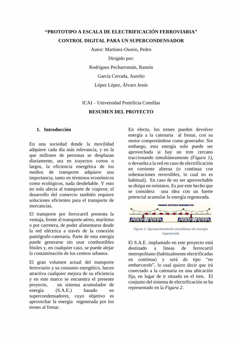
“PROTOTIPO A ESCALA DE ELECTRIFICACIÓN FERROVIARIA” CONTROL DIGITAL PARA UN SUPERCONDENSADOR Autor: Martínez-Osorio, Pedro Dirigido por: Rodríguez Pecharromán, Ramón García Cerrada, Aurelio López López, Álvaro Jesús ICAI – Universidad Pontificia Comillas RESUMEN DEL PROYECTO 1. Introducción En una sociedad donde la movilidad adquiere cada día más relevancia, y en la que millones de personas se desplazan diariamente, sea en trayectos cortos o largos, la eficiencia energética de los medios de transporte adquiere una importancia, tanto en términos económicos como ecológicos, nada desdeñable. Y esto no solo afecta al transporte de viajeros: el desarrollo del comercio también requiere soluciones eficientes para el transporte de mercancías. El transporte por ferrocarril presenta la ventaja, frente al transporte aéreo, marítimo o por carretera, de poder alimentarse desde la red eléctrica a través de la conexión pantógrafo-catenaria. Parte de esta energía puede generarse sin usar combustibles fósiles y, en cualquier caso, se puede alejar la contaminación de los centros urbanos. El gran volumen actual del transporte ferroviario y su consumo energético, hacen atractiva cualquier mejora de su eficiencia y en este marco se encuentra el presente proyecto, un sistema acumulador de energía (S.A.E.) basado en supercondensadores, cuyo objetivo es aprovechar la energía regenerada por los trenes al frenar. En efecto, los trenes pueden devolver energía a la catenaria al frenar, con su motor comportándose como generador. Sin embargo, esta energía solo puede ser aprovechada si hay un tren cercano traccionando simultáneamente (Figura 1), o devuelta a la red en caso de electrificación en corriente alterna (o continua con subestaciones reversibles, lo cual no es habitual). En caso de no ser aprovechable se disipa en reóstatos. Es por este hecho que se considera una idea con un fuerte potencial acumular la energía regenerada. Figura 1: Aprovechamiento simultáneo de energía regenerada El S.A.E. implantado en este proyecto está destinado a líneas de ferrocarril metropolitano (habitualmente electrificadas en continua) y será de tipo “no embarcardo”, lo cual quiere decir que irá conectado a la catenaria en una ubicación fija, en lugar de ir situado en el tren. El conjunto del sistema de electrificación se ha representado en la Figura 2.
Transcript of PROTOTIPO A ESCALA DE ELECTRIFICACIÓN FERROVIARIA … · circuitos de filtrado basados en filtros...
“PROTOTIPO A ESCALA DE ELECTRIFICACIÓN FERROVIARIA”
CONTROL DIGITAL PARA UN SUPERCONDENSADOR
Autor: Martínez-Osorio, Pedro
Dirigido por:
Rodríguez Pecharromán, Ramón
García Cerrada, Aurelio
López López, Álvaro Jesús
ICAI – Universidad Pontificia Comillas
RESUMEN DEL PROYECTO
1. Introducción
En una sociedad donde la movilidad
adquiere cada día más relevancia, y en la
que millones de personas se desplazan
diariamente, sea en trayectos cortos o
largos, la eficiencia energética de los
medios de transporte adquiere una
importancia, tanto en términos económicos
como ecológicos, nada desdeñable. Y esto
no solo afecta al transporte de viajeros: el
desarrollo del comercio también requiere
soluciones eficientes para el transporte de
mercancías.
El transporte por ferrocarril presenta la
ventaja, frente al transporte aéreo, marítimo
o por carretera, de poder alimentarse desde
la red eléctrica a través de la conexión
pantógrafo-catenaria. Parte de esta energía
puede generarse sin usar combustibles
fósiles y, en cualquier caso, se puede alejar
la contaminación de los centros urbanos.
El gran volumen actual del transporte
ferroviario y su consumo energético, hacen
atractiva cualquier mejora de su eficiencia
y en este marco se encuentra el presente
proyecto, un sistema acumulador de
energía (S.A.E.) basado en
supercondensadores, cuyo objetivo es
aprovechar la energía regenerada por los
trenes al frenar.
En efecto, los trenes pueden devolver
energía a la catenaria al frenar, con su
motor comportándose como generador. Sin
embargo, esta energía solo puede ser
aprovechada si hay un tren cercano
traccionando simultáneamente (Figura 1),
o devuelta a la red en caso de electrificación
en corriente alterna (o continua con
subestaciones reversibles, lo cual no es
habitual). En caso de no ser aprovechable
se disipa en reóstatos. Es por este hecho que
se considera una idea con un fuerte
potencial acumular la energía regenerada.
Figura 1: Aprovechamiento simultáneo de energía regenerada
El S.A.E. implantado en este proyecto está
destinado a líneas de ferrocarril
metropolitano (habitualmente electrificadas
en continua) y será de tipo “no
embarcardo”, lo cual quiere decir que irá
conectado a la catenaria en una ubicación
fija, en lugar de ir situado en el tren. El
conjunto del sistema de electrificación se ha
representado en la Figura 2.
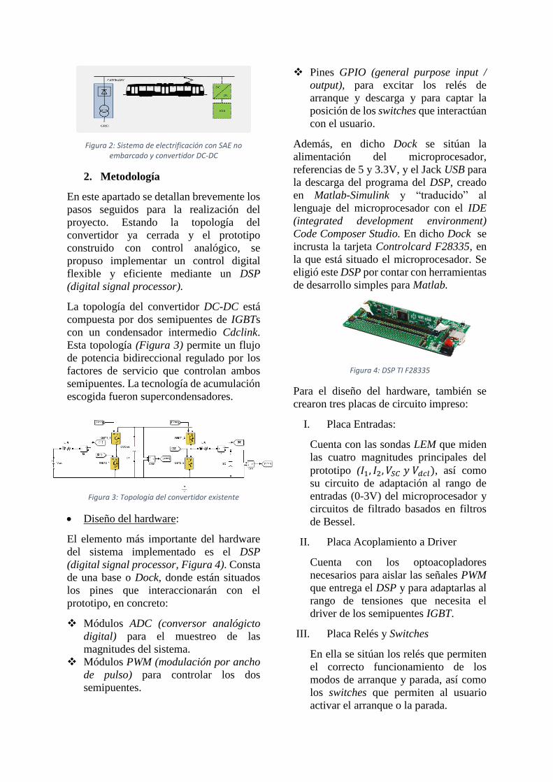
Figura 2: Sistema de electrificación con SAE no embarcado y convertidor DC-DC
2. Metodología
En este apartado se detallan brevemente los
pasos seguidos para la realización del
proyecto. Estando la topología del
convertidor ya cerrada y el prototipo
construido con control analógico, se
propuso implementar un control digital
flexible y eficiente mediante un DSP
(digital signal processor).
La topología del convertidor DC-DC está
compuesta por dos semipuentes de IGBTs
con un condensador intermedio Cdclink.
Esta topología (Figura 3) permite un flujo
de potencia bidireccional regulado por los
factores de servicio que controlan ambos
semipuentes. La tecnología de acumulación
escogida fueron supercondensadores.
Figura 3: Topología del convertidor existente
Diseño del hardware:
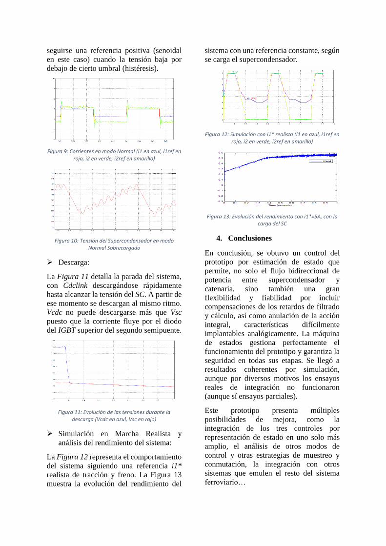
El elemento más importante del hardware
del sistema implementado es el DSP
(digital signal processor, Figura 4). Consta
de una base o Dock, donde están situados
los pines que interaccionarán con el
prototipo, en concreto:
Módulos ADC (conversor analógicto
digital) para el muestreo de las
magnitudes del sistema.
Módulos PWM (modulación por ancho
de pulso) para controlar los dos
semipuentes.
Pines GPIO (general purpose input /
output), para excitar los relés de
arranque y descarga y para captar la
posición de los switches que interactúan
con el usuario.
Además, en dicho Dock se sitúan la
alimentación del microprocesador,
referencias de 5 y 3.3V, y el Jack USB para
la descarga del programa del DSP, creado
en Matlab-Simulink y “traducido” al
lenguaje del microprocesador con el IDE
(integrated development environment)
Code Composer Studio. En dicho Dock se
incrusta la tarjeta Controlcard F28335, en
la que está situado el microprocesador. Se
eligió este DSP por contar con herramientas
de desarrollo simples para Matlab.
Figura 4: DSP TI F28335
Para el diseño del hardware, también se
crearon tres placas de circuito impreso:
I. Placa Entradas:
Cuenta con las sondas LEM que miden
las cuatro magnitudes principales del
prototipo (𝐼1, 𝐼2, 𝑉𝑆𝐶 𝑦 𝑉𝑑𝑐𝑙), así como
su circuito de adaptación al rango de
entradas (0-3V) del microprocesador y
circuitos de filtrado basados en filtros
de Bessel.
II. Placa Acoplamiento a Driver
Cuenta con los optoacopladores
necesarios para aislar las señales PWM
que entrega el DSP y para adaptarlas al
rango de tensiones que necesita el
driver de los semipuentes IGBT.
III. Placa Relés y Switches
En ella se sitúan los relés que permiten
el correcto funcionamiento de los
modos de arranque y parada, así como
los switches que permiten al usuario
activar el arranque o la parada.

Diseño del control:
Se decidió cambiar los controles PI
analógicos existentes por controles por
representación de estado que permitieran,
además de aplicar la acción integral,
compensar retardos en el filtrado (se
eligieron filtros de Bessel) y en el cálculo
del control. En total habrá tres controles,
resumidos en la Tabla 1:
Control Misión Referencia Medida Salida
1 Seguir
referencia i1*
i1* i1 D1
2 Mantener
Vcdclink cte
Vcdcnom Vcdc i2*
3 Seguir
referencia i2*
i2* i2 D2
Tabla 1: Resumen de controles
Del la topología del sistema (Figura 3) se
extrajeron las relaciones (1), (2) y (3).
𝑑𝑖1
𝑑𝑡= −
𝑅1
𝐿1· 𝑖1 +
𝑉𝐶𝐴𝑇−𝑉𝐴
𝐿1 (1)
𝑑
𝑑𝑡𝑉𝑐𝑑𝑐𝑙𝑖𝑛𝑘
2 =2
𝐶(𝑃𝐼 − 𝑃𝐷)
(2)
𝑑𝑖2
𝑑𝑡= −
𝑅2
𝐿2
· 𝑖2 +𝑉𝐵 − 𝑉𝑆𝐶
𝐿2
(3)
De donde se derivan los tres controles,
definidos matricialmente por (4), (5) y (6).
(4)
(5)
(6)
Finalmente, es posible calcular D1, i2ref y
D2, a partir de los tres controles u1, u2 y u3
según descrito en (7),(8) y (9).
𝑢1 =𝑉𝐶𝐴𝑇−𝑉𝐴
𝐿1 𝐷1 = 1 −
𝑉𝐴
𝑉𝑑𝑐𝑙𝑖𝑛𝑘𝑓⁄ (7)
𝑢2 =2
𝐶(𝑃𝐼 − 𝑃𝐷) 𝐼2
𝑟𝑒𝑓=
𝑃𝐷
𝑉𝑆𝐶
(8)
𝑢3 =𝑉𝐵−𝑉𝑆𝐶
𝐿2 𝐷2 = 1 −
𝑉𝐵
𝑉𝑑𝑐𝑙𝑖𝑛𝑘𝑓⁄
(9)
Donde los superíndices f y c representan,
respectivamente, las señales filtrada y
calculada. 𝜁, por su parte, será la acción
integral, que podrá ser anulada en el
diagrama de bloques de los controles para
mejorar su comportamiento en caso de
saturación de la salida.
En resumen, el flujo del control es el
siguiente: una referencia externa i1* (que
también es posible introducir internamente
en el programa del DSP) determina la
corriente que el SAE capta o devuelve a la
catenaria y es seguida por el Control 1. El
Control 2 se encarga de regular la tensión
del condensador intermedio generando una
consigna de corriente i2* que será seguida
por el Control 3, cargando o descargando el
supercondensador.
Estrategia de muestreo y conmutación:
Se trata de conseguir una estrategia que
aproveche toda la flexibilidad que otorga un
control digital. De esta manera se diseñó la
estructura del programa del DSP de manera
que fuera posible elegir cada cuántos ciclos
de conmutación se muestrea (con fswitch
múltiplo de fsampl).
Por otro lado, se diseñan los módulos
ePWM del programa del DSP para que los
flancos de la señal cuadrada no coincidan
con el muestreo, puesto que introducirían
ruido en la señal muestreada que podría dar
lugar a errores relevantes. Para ello se sigue
una lógica up-down con las acciones de
SET y CLEAR siempre en puntos
intermedios del período, nunca al inicio o al
final, como se describe en la Figura 5.

Figura 5: Estrategia señal PWM
Máquina de estados
Se dotó al programa del DSP de una
máquina de estados (Figura 6) en Stateflow
para gestionar los distintos modos de
funcionamiento del sistema. En general
habrá tres grandes modos:
Figura 6: Máquina de estados del programa del DSP
I. Modo arranque:
Se inicia desde el estado “Standby” al
actuar sobre un interruptor, y su objetivo es
llevar el prototipo a sus condiciones
habituales de funcionamiento, con ambos
condensadores a una tensión cercana a su
tensión nominal. Tendrá lugar en varias
etapas: en primer lugar se cargará el
condensador intermedio hasta Vcat a través
del llamado relé de arranque,
posteriormente el primer semipuente
empieza a conmutar para llevarlo a una
tensión superior a la de catenaria. Por
último, el segundo semipuente empieza a
conmutar para cargar el supercondensador,
carga que será mucho más lenta por su gran
capacidad.
II. Modo normal:
Es el modo habitual de funcionamiento del
prototipo, en el que se sigue la referencia de
corriente de catenaria i1*. Presenta dos
subestados: cuando la tensión del
supercondensador sea demasiado elevada
sólo se seguirán consignas negativas, y
cuando sea demasiado baja, sólo se
seguirán consignas positivas. En ambos
casos se dota a la máquina de histéresis para
mejorar su funcionamiento.
III. Modo parada:
Se inicia desde cualquier estado al actuar
sobre el interruptor de parada, o al
sobrepasar umbrales muy altos de tensiones
e intensidades. Cierra el relé de descarga
del supercondensador y dipara el IGBT de
descarga del condensador intermedio. Se
trata de un modo predominante, al cual se
entra desde cualquier estado y bajo
cualquier condición por motivos de
seguridad. Su objetivo es descargar
completamente el sistema.
3. Resultados
Se obtuvieron los siguientes resultados por
simulación:
Arranque: en la Figura 7 y la Figura 8
se detalla el arranque del sistema hasta
entrar en modo Normal.
Figura 7: Corrientes en el Arranque (i1 en azul, i1ref en rojo, i2 en verde, i2ref en amarillo)
Figura 8: Tensiones en el Arranque (Vsc en rojo, Vcdc en azul)
Modo Normal:
En la Figura 9 se detalla el seguimiento de
una referencia i1* cuadrada, mientras que
en la Figura 10 puede apreciarse cómo, en
modo normal sobrecargado, sólo vuelve a
seguirse una referencia positiva (senoidal
en este caso) cuando la tensión baja por
debajo de cierto umbral (histéresis).
Figura 9: Corrientes en modo Normal (i1 en azul, i1ref en rojo, i2 en verde, i2ref en amarillo)
Figura 10: Tensión del Supercondensador en modo Normal Sobrecargado
Descarga:
La Figura 11 detalla la parada del sistema,
con Cdclink descargándose rápidamente
hasta alcanzar la tensión del SC. A partir de
ese momento se descargan al mismo ritmo.
Vcdc no puede descargarse más que Vsc
puesto que la corriente fluye por el diodo
del IGBT superior del segundo semipuente.
Figura 11: Evolución de las tensiones durante la descarga (Vcdc en azul, Vsc en rojo)
Simulación en Marcha Realista y
análisis del rendimiento del sistema:
La Figura 12 representa el comportamiento
del sistema siguiendo una referencia i1*
realista de tracción y freno. La Figura 13
muestra la evolución del rendimiento del
sistema con una referencia constante, según
se carga el supercondensador.
Figura 12: Simulación con i1* realista (i1 en azul, i1ref en rojo, i2 en verde, i2ref en amarillo)
Figura 13: Evolución del rendimiento con i1*=5A, con la carga del SC
4. Conclusiones
En conclusión, se obtuvo un control del
prototipo por estimación de estado que
permite, no solo el flujo bidireccional de
potencia entre supercondensador y
catenaria, sino también una gran
flexibilidad y fiabilidad por incluir
compensaciones de los retardos de filtrado
y cálculo, así como anulación de la acción
integral, características difícilmente
implantables analógicamente. La máquina
de estados gestiona perfectamente el
funcionamiento del prototipo y garantiza la
seguridad en todas sus etapas. Se llegó a
resultados coherentes por simulación,
aunque por diversos motivos los ensayos
reales de integración no funcionaron
(aunque sí ensayos parciales).
Este prototipo presenta múltiples
posibilidades de mejora, como la
integración de los tres controles por
representación de estado en uno solo más
amplio, el análisis de otros modos de
control y otras estrategias de muestreo y
conmutación, la integración con otros
sistemas que emulen el resto del sistema
ferroviario…
“RAILWAY ELECTRIFICATION SCALED PROTOTYPE”
DIGITAL CONTROL FOR A SUPERCAPACITOR
Author: Martínez-Osorio, Pedro
Directors:
Rodríguez Pecharromán, Ramón
García Cerrada, Aurelio
López López, Álvaro Jesús
ICAI – Universidad Pontificia Comillas
ABSTRACT
1. Introduction
Mobility is crucial to today’s society, with
millions of people commuting and
travelling every day. In this context, the
efficiency of the means of conveyance has
an importance that cannot be neglected,
both in economic and ecologic terms. This
matter does not only concern passenger
transport: commerce also requires efficient
solutions for freight transport.
Rail transport has the advantage, as
opposed to air, maritime or road transport,
of being able to get its energy from the
power grid through the catenary-
pantograph connection. Part of this energy
can be generated without fossil fuel and
pollution can be kept out of urban centres.
The massive energetic consumption of rail
systems makes any efficiency improvement
extremely attractive. In such a context, the
present project aims to harness braking
energy from trains and store it in an E.S.S.
(energy storage system) based on
supercapacitors.
Trains can return energy to the catenary
when they brake, with their engines
behaving as a generator. However, this
energy can only be used if there is a nearby
train accelerating simultaneously (Figure
1). It can also be returned to the power grid
in AC electrification systems (or DC
systems with reversible substations, which
are rather uncommon). If these conditions
cannot be fulfilled, energy will be
dissipated in resistors: this is why storage
systems for the regenerated energy have a
big potential.
Figure 1: Regenerative braking energy flow
The E.S.S. implemented in this project is
intended for metropolitan railways (usually
electrified in DC). It will be a wayside
system, which means it will be connected to
the catenary in a fixed position, instead of
being set on board. The entire
electrification system is shown in Figure 2.
Figure 2: Electrification system with a wayside ESS and a DC-DC converter.
2. Methodology
This section deals with the main steps of the
project. As the converter topology was

already defined and a prototype with analog
controls had already been built, the next
step was to implement a digital control
based on a DSP (digital signal processor).
The DC-DC converter is made up by two
IGBT half bridges, with an intermediate
capacitor Cdclink. This topology (Figure 3)
allows power flow in both directions,
regulated by the duty cycles that control
both half bridges.
Figure 3: Topology of the DC-DC converter
Hardware design:
The most important element of the control
system is a DSP (digital signal processor,
Figure 4). The pins that interact with the
prototype are situated in the DSP docking
station:
ADC modules (analog-to-digital
converter) to sample the system’s
magnitudes.
PWM modules (pulse width
modulation) to control the half bridges.
GPIO pins (general purpose input /
output), outputs to excite the start-stop
relays and inputs to interact with the
user through switches.
Said docking station also houses the power
supply, 5 and 3.3V references, and a USB
connector to download programs into the
DSP. Such programs will be created with
Matlab-Simulink and “translated” into the
microprocessor language by an IDE
(integrated development environment)
called Code Composer Studio (CCS). The
microprocessor is part of the Controlcard
F28335, which is meant to be inserted in the
dock. The main reason to choose this DSP
were its simple development tools for
Matlab.
Figure 4: DSP TI F28335
As a part of the hardware design, three
printed circuit boards (PCB) were created:
I. Board “Inputs”:
It houses the LEM transducers that
measure the four main magnitudes of
the prototype (𝐼1, 𝐼2, 𝑉𝑆𝐶 𝑦 𝑉𝑑𝑐𝑙), as well
as the circuit to adapt them to the ADC
range (0-3V) and Bessel filtering
circuits.
II. Board “Driver Coupling”
It contains optocoupling circuits to
isolate and adapt the PWM signals that
control the IGBT half bridges.
III. Board “Relays and Switches”
It houses the relays that ensure a correct
start and stop of the prototype, as well
as the switches that interact with the
user.
Control design:
The existing PI analog controls were
replaced by state-representation controls
that implement, as well as the integral
action, compensations for filtering and
control delays. There are three controls, as
shown in Table 1:
Control Objective Referencie Input Output
1 Follow
reference i1*
i1* i1 D1
2 Keep Vcdclink
constant
Vcdcnom Vcdc i2*
3 Follow
reference i2*
i2* i2 D2
Table 1: Controls
From the system topology (Figure 3)
relations (1), (2) and (3) can be deduced.
𝑑𝑖1
𝑑𝑡= −
𝑅1
𝐿1· 𝑖1 +
𝑉𝐶𝐴𝑇−𝑉𝐴
𝐿1 (1)
𝑑
𝑑𝑡𝑉𝑐𝑑𝑐𝑙𝑖𝑛𝑘
2 =2
𝐶(𝑃𝐼 − 𝑃𝐷)
(2)
𝑑𝑖2
𝑑𝑡= −
𝑅2
𝐿2
· 𝑖2 +𝑉𝐵 − 𝑉𝑆𝐶
𝐿2
(3)
From those equations, the matrix state
representation of each control is developed
as shown in (4), (5) and (6).
(4)
(5)
(6)
Finally, D1, i2ref and D2 are calculated
from controls u1, u2 y u3 as shown in (7),
(8) and (9).
𝑢1 =𝑉𝐶𝐴𝑇−𝑉𝐴
𝐿1 𝐷1 = 1 −
𝑉𝐴
𝑉𝑑𝑐𝑙𝑖𝑛𝑘𝑓⁄ (7)
𝑢2 =2
𝐶(𝑃𝐼 − 𝑃𝐷) 𝐼2
𝑟𝑒𝑓=
𝑃𝐷
𝑉𝑆𝐶
(8)
𝑢3 =𝑉𝐵−𝑉𝑆𝐶
𝐿2 𝐷2 = 1 −
𝑉𝐵
𝑉𝑑𝑐𝑙𝑖𝑛𝑘𝑓⁄
(9)
Where f and c superindexes represent
filtered and calculated signals. 𝜁 represents
the integral action, that can be annulated in
the controls block diagrams to improve
their behaviour in case of output saturation.
In summary, the control works as follows:
an external reference i1* (which can also be
internally introduced in the DSP program)
determines the current that flows between
ESS and catenary. Such reference is
followed by Control 1. Control 2 is in
charge of regulating the voltage of the
intermediate capacitor, generating a current
reference i2* that will be followed Control
3, hence charging or discharging the
supercapacitor.
Sampling and switching strategy:
Sampling and switching strategies should
benefit from the flexibility that a digital
control allows. The structure of the DSP
program was created in such a way that it is
possible to choose the number of switching
periods between samplings (fswitch will be
a multiple of fsampl).
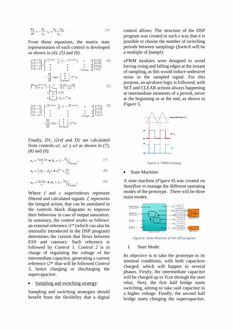
ePWM modules were designed to avoid
having rising and falling edges at the instant
of sampling, as this would induce undesired
noise in the sampled signal. For this
purpose, an up-down logic is followed, with
SET and CLEAR actions always happening
at intermediate moments of a period, never
at the beginning or at the end, as shown in
Figure 5.
Figure 5: PWM strategy
State Machine:
A state machine (Figure 6) was created on
Stateflow to manage the different operating
modes of the prototype. There will be three
main modes:
Figure 6: State Machine of the DSP program
I. Start Mode:
Its objective is to take the prototype to its
nominal conditions, with both capacitors
charged, which will happen in several
phases. Firstly, the intermediate capacitor
will be charged up to Vcat through the start
relay. Next, the first half bridge starts
switching, aiming to take said capacitor to
a higher voltage. Finally, the second half
bridge starts charging the supercapacitor.
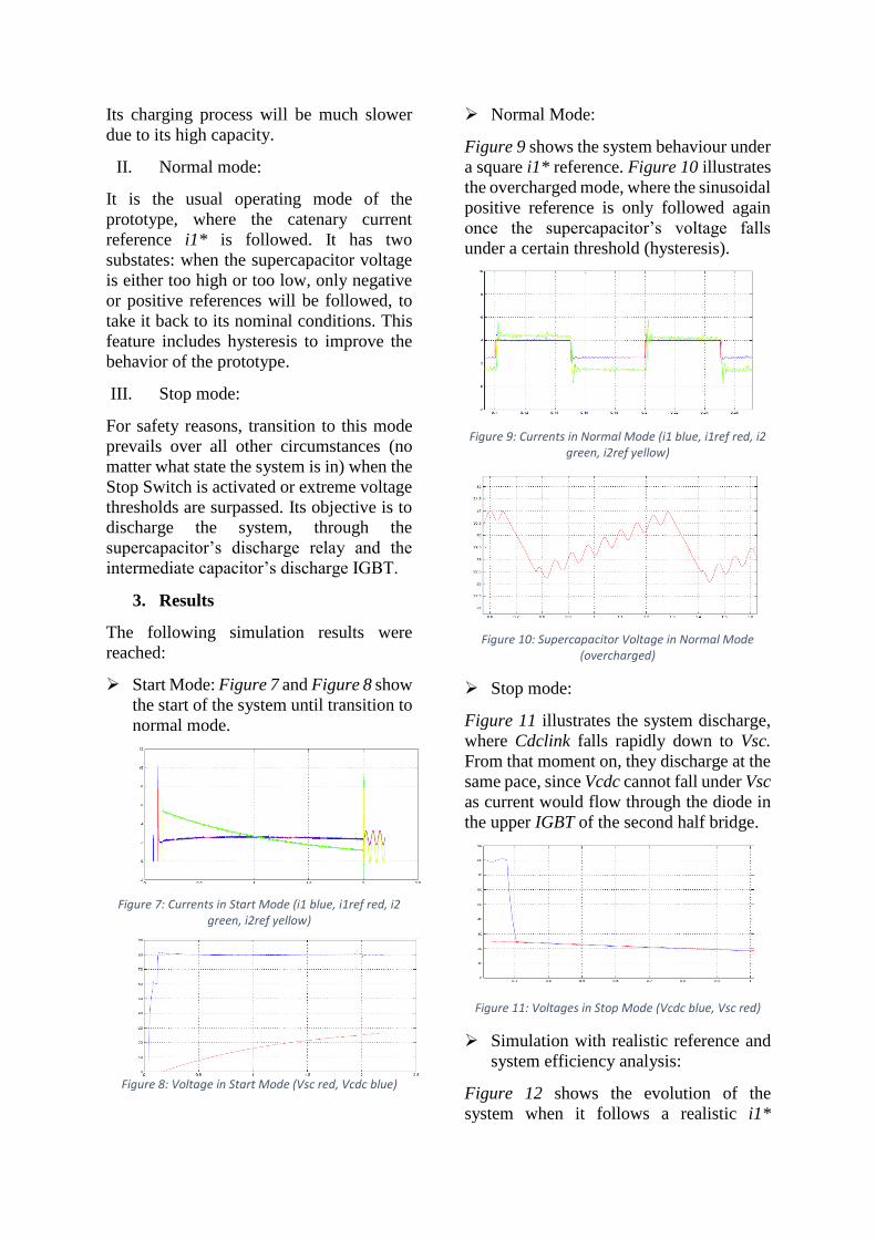
Its charging process will be much slower
due to its high capacity.
II. Normal mode:
It is the usual operating mode of the
prototype, where the catenary current
reference i1* is followed. It has two
substates: when the supercapacitor voltage
is either too high or too low, only negative
or positive references will be followed, to
take it back to its nominal conditions. This
feature includes hysteresis to improve the
behavior of the prototype.
III. Stop mode:
For safety reasons, transition to this mode
prevails over all other circumstances (no
matter what state the system is in) when the
Stop Switch is activated or extreme voltage
thresholds are surpassed. Its objective is to
discharge the system, through the
supercapacitor’s discharge relay and the
intermediate capacitor’s discharge IGBT.
3. Results
The following simulation results were
reached:
Start Mode: Figure 7 and Figure 8 show
the start of the system until transition to
normal mode.
Figure 7: Currents in Start Mode (i1 blue, i1ref red, i2 green, i2ref yellow)
Figure 8: Voltage in Start Mode (Vsc red, Vcdc blue)
Normal Mode:
Figure 9 shows the system behaviour under
a square i1* reference. Figure 10 illustrates
the overcharged mode, where the sinusoidal
positive reference is only followed again
once the supercapacitor’s voltage falls
under a certain threshold (hysteresis).
Figure 9: Currents in Normal Mode (i1 blue, i1ref red, i2 green, i2ref yellow)
Figure 10: Supercapacitor Voltage in Normal Mode (overcharged)
Stop mode:
Figure 11 illustrates the system discharge,
where Cdclink falls rapidly down to Vsc.
From that moment on, they discharge at the
same pace, since Vcdc cannot fall under Vsc
as current would flow through the diode in
the upper IGBT of the second half bridge.
Figure 11: Voltages in Stop Mode (Vcdc blue, Vsc red)
Simulation with realistic reference and
system efficiency analysis:
Figure 12 shows the evolution of the
system when it follows a realistic i1*
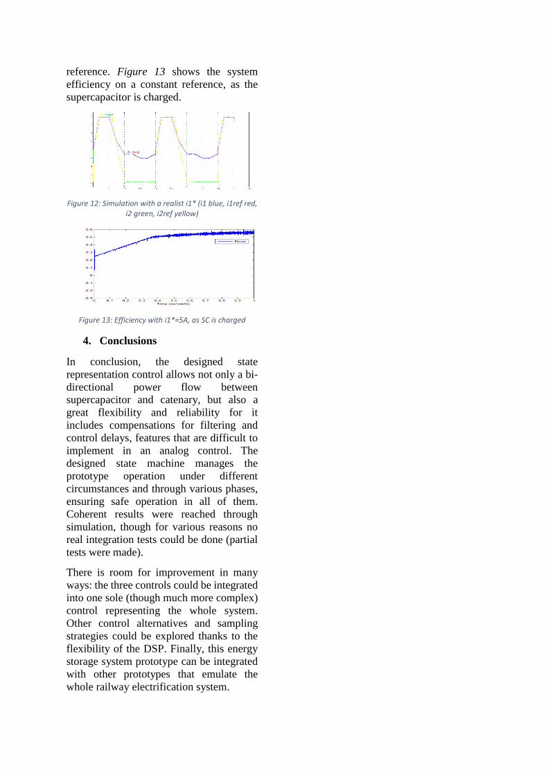
reference. Figure 13 shows the system
efficiency on a constant reference, as the
supercapacitor is charged.
Figure 12: Simulation with a realist i1* (i1 blue, i1ref red, i2 green, i2ref yellow)
Figure 13: Efficiency with i1*=5A, as SC is charged
4. Conclusions
In conclusion, the designed state
representation control allows not only a bi-
directional power flow between
supercapacitor and catenary, but also a
great flexibility and reliability for it
includes compensations for filtering and
control delays, features that are difficult to
implement in an analog control. The
designed state machine manages the
prototype operation under different
circumstances and through various phases,
ensuring safe operation in all of them.
Coherent results were reached through
simulation, though for various reasons no
real integration tests could be done (partial
tests were made).
There is room for improvement in many
ways: the three controls could be integrated
into one sole (though much more complex)
control representing the whole system.
Other control alternatives and sampling
strategies could be explored thanks to the
flexibility of the DSP. Finally, this energy
storage system prototype can be integrated
with other prototypes that emulate the
whole railway electrification system.