
Time-of-Flight sensors in standard CMOS technologies · Outline ToF sensors in standard CMOS...
59
citius.usc.es Centro Singular de Investigación en Tecnoloxías da Información UNIVERSIDADE DE SANTIAGO DE COMPOSTELA Time-of-Flight sensors in standard CMOS technologies Julio Illade Quinteiro
Transcript of Time-of-Flight sensors in standard CMOS technologies · Outline ToF sensors in standard CMOS...

citius.usc.es
Centro Singular de Investigación en Tecnoloxías da Información
UNIVERSIDADE DE SANTIAGO DE COMPOSTELA
Time-of-Flight sensors in standard CMOS technologies
Julio Illade Quinteiro
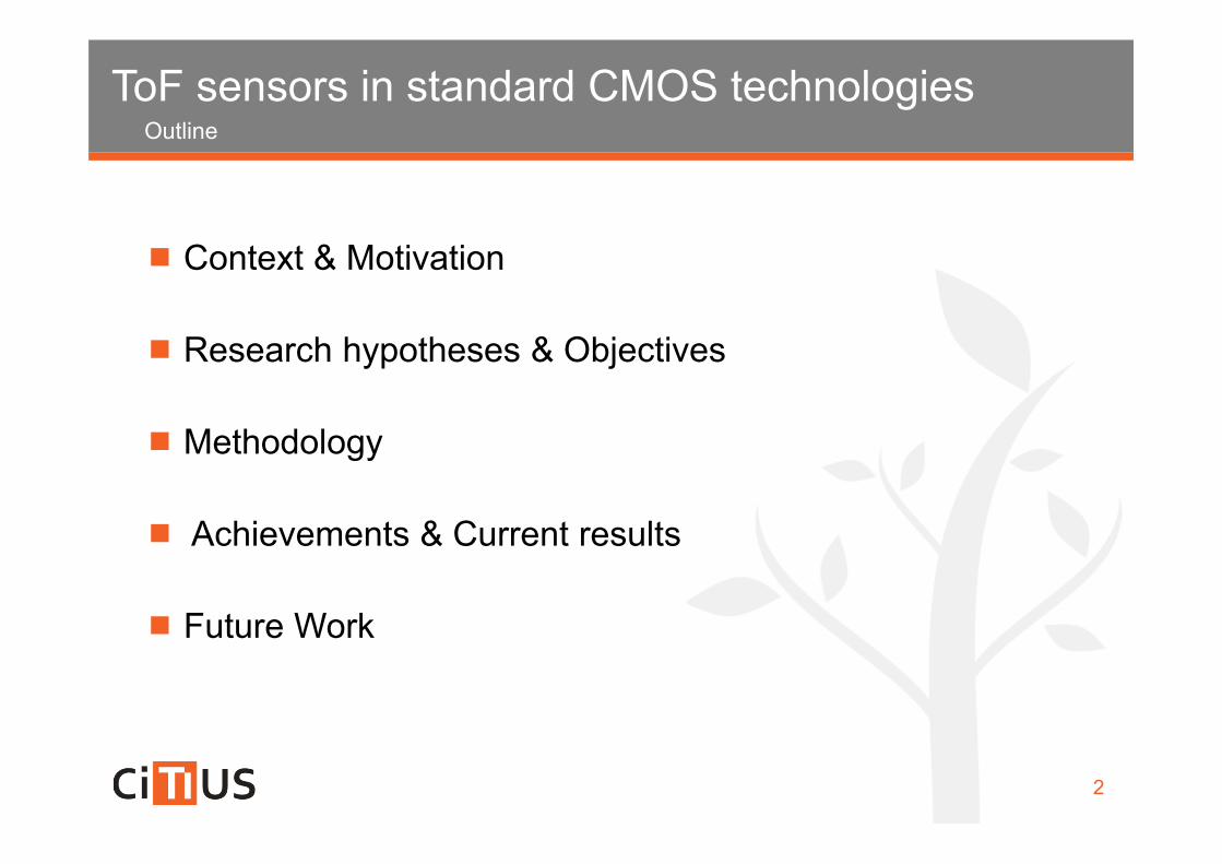
OutlineToF sensors in standard CMOS technologies
2
Context & Motivation
Research hypotheses & Objectives
Methodology
Achievements & Current results
Future Work
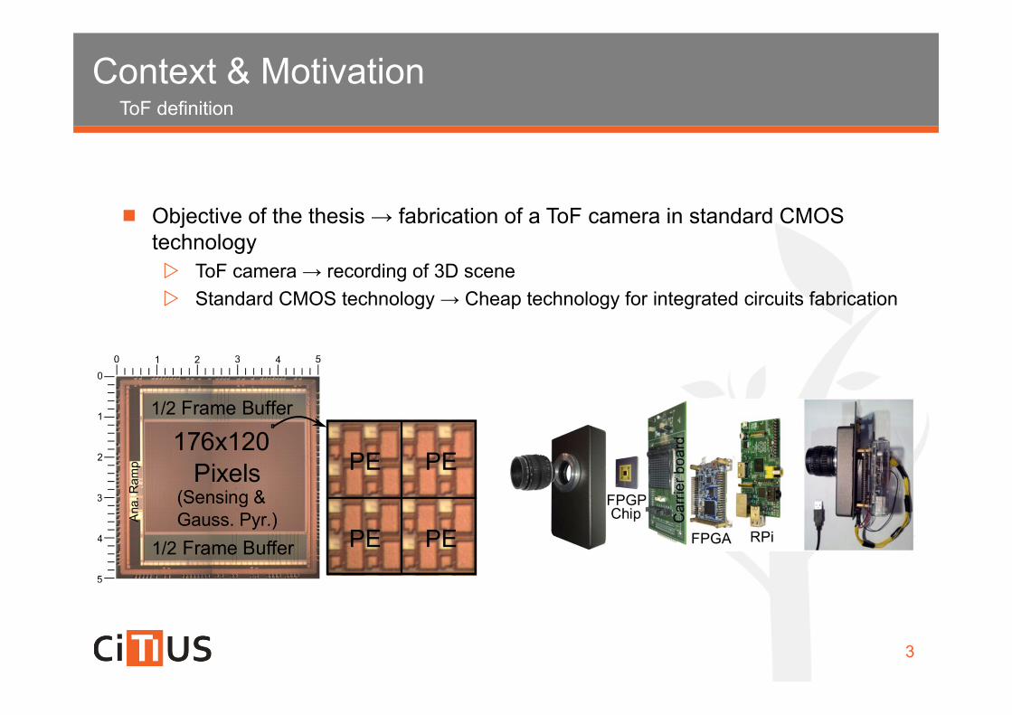
ToF definitionContext & Motivation
3
Objective of the thesis → fabrication of a ToF camera in standard CMOS technology ToF camera → recording of 3D scene Standard CMOS technology → Cheap technology for integrated circuits fabrication
ToF definitionContext & Motivation
4
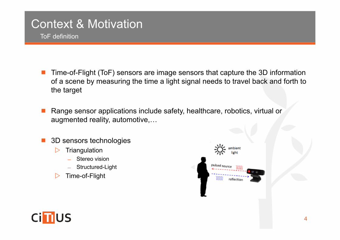
Time-of-Flight (ToF) sensors are image sensors that capture the 3D information of a scene by measuring the time a light signal needs to travel back and forth to the target
Range sensor applications include safety, healthcare, robotics, virtual or augmented reality, automotive,…
3D sensors technologies Triangulation
Stereo vision Structured-Light
Time-of-Flight
3D sensors technologiesContext & Motivation
5
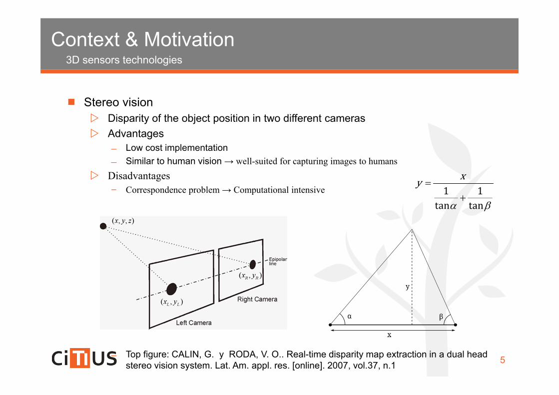
Stereo vision Disparity of the object position in two different cameras Advantages
Low cost implementation Similar to human vision → well-suited for capturing images to humans
Disadvantages Correspondence problem → Computational intensive
Top figure: CALIN, G. y RODA, V. O.. Real-time disparity map extraction in a dual head stereo vision system. Lat. Am. appl. res. [online]. 2007, vol.37, n.1
1 1tan tan
xy
3D sensors technologiesContext & Motivation
6
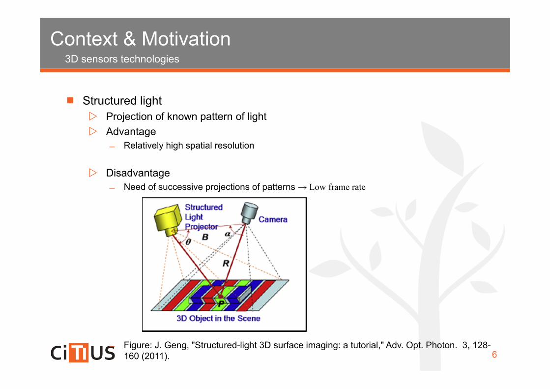
Structured light Projection of known pattern of light Advantage
Relatively high spatial resolution
Disadvantage Need of successive projections of patterns → Low frame rate
Figure: J. Geng, "Structured-light 3D surface imaging: a tutorial," Adv. Opt. Photon. 3, 128-160 (2011).
3D sensors technologiesContext & Motivation
7
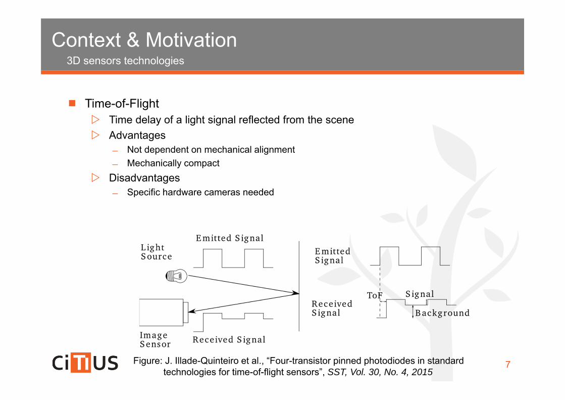
Time-of-Flight Time delay of a light signal reflected from the scene Advantages
Not dependent on mechanical alignment Mechanically compact
Disadvantages Specific hardware cameras needed
Figure: J. Illade-Quinteiro et al., “Four-transistor pinned photodiodes in standardtechnologies for time-of-flight sensors”, SST, Vol. 30, No. 4, 2015
3D sensors technologiesContext & Motivation
8
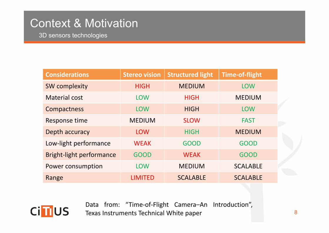
Considerations Stereo vision Structured light Time‐of‐flight
SW complexity HIGH MEDIUM LOW
Material cost LOW HIGH MEDIUM
Compactness LOW HIGH LOW
Response time MEDIUM SLOW FAST
Depth accuracy LOW HIGH MEDIUM
Low‐light performance WEAK GOOD GOOD
Bright‐light performance GOOD WEAK GOOD
Power consumption LOW MEDIUM SCALABLE
Range LIMITED SCALABLE SCALABLE
Data from: “Time‐of‐Flight Camera–An Introduction”,Texas Instruments Technical White paper
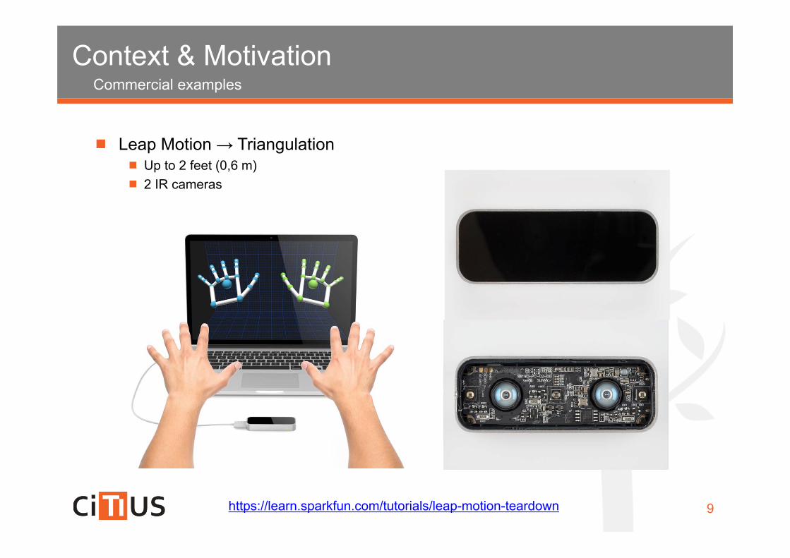
Commercial examplesContext & Motivation
9
Leap Motion → Triangulation Up to 2 feet (0,6 m) 2 IR cameras
https://learn.sparkfun.com/tutorials/leap-motion-teardown
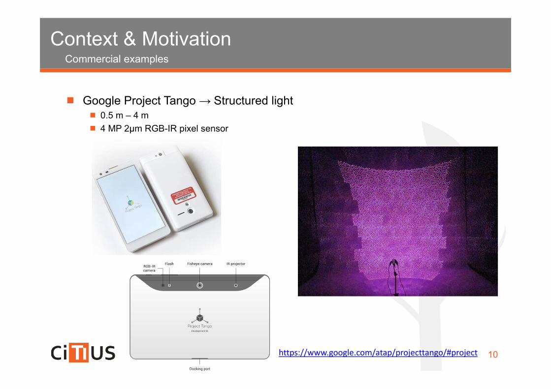
Commercial examplesContext & Motivation
10
Google Project Tango → Structured light 0.5 m – 4 m 4 MP 2µm RGB-IR pixel sensor
https://www.google.com/atap/projecttango/#project
Commercial examplesContext & Motivation
11
Intel RealSense→ Structured light 0.2 m – 1.2 m 1080p RGB-IR
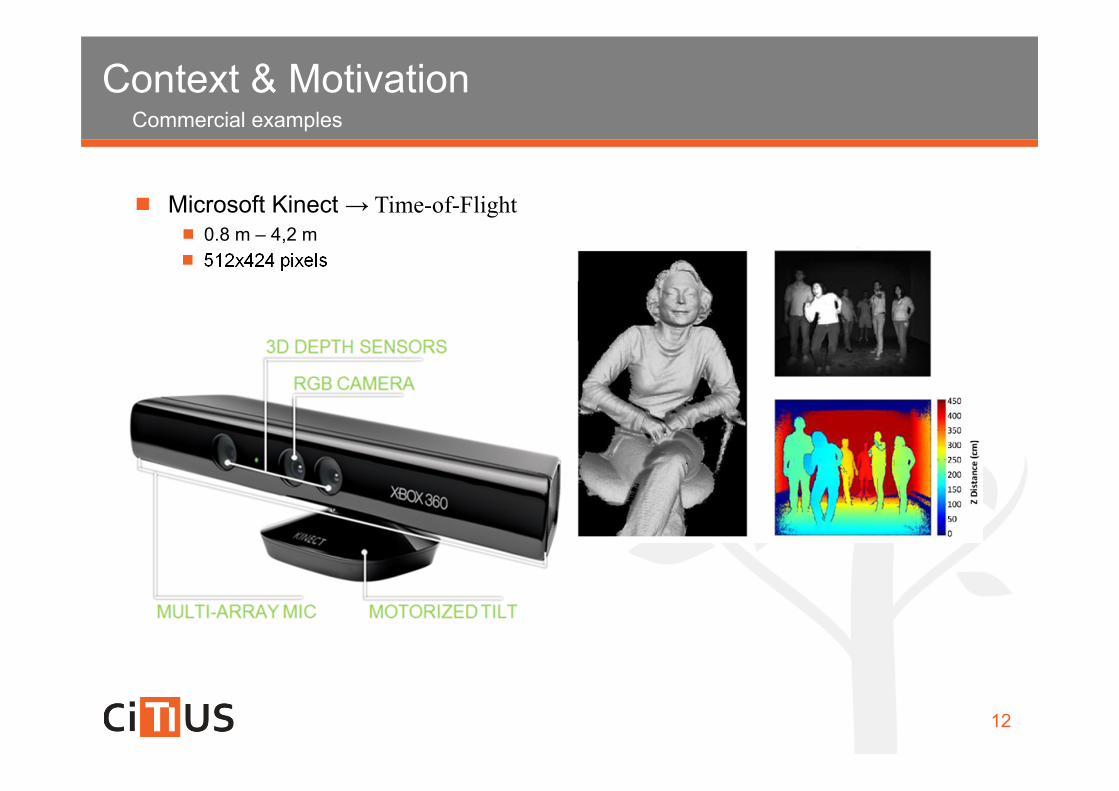
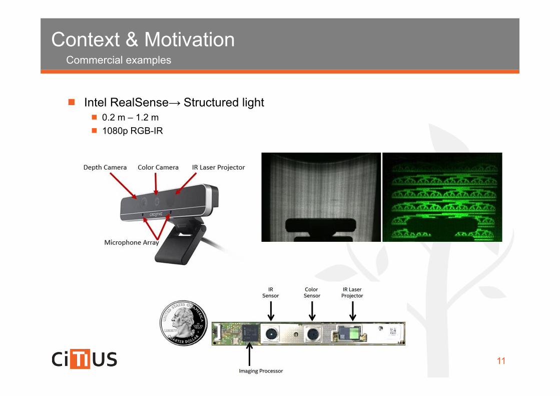
Commercial examplesContext & Motivation
12
Microsoft Kinect → Time-of-Flight 0.8 m – 4,2 m 512x424 pixels
Research hypotheses & Objectives
13
ToF measurement technique
Conventional image sensor pixels
Silicon photosensors
3-Transistors (3T) pixel
4-Transistors (4T) pixel
4T pixel for ToF
4T pixel in standard CMOS technology

ToF measurement techniqueResearch hypotheses & Objectives
14
Time-of-Flight sensors measure the time a light signal needs to travel back and forth to the target
The light signal can be continuous modulated wave discrete pulses
We will center this presentation in the pulsed ToF
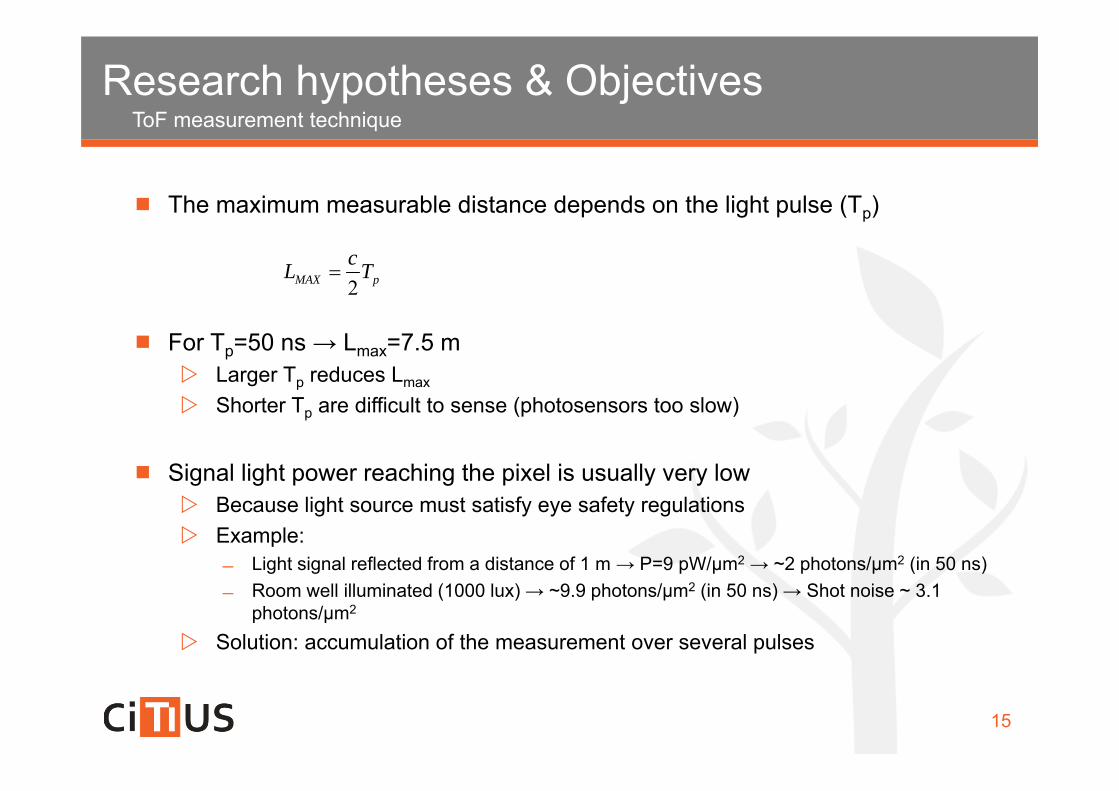
The maximum measurable distance depends on the light pulse (Tp)
2 oFcL T
2MAX pcL T
ToF measurement techniqueResearch hypotheses & Objectives
15
The maximum measurable distance depends on the light pulse (Tp)
For Tp=50 ns → Lmax=7.5 m Larger Tp reduces Lmax
Shorter Tp are difficult to sense (photosensors too slow)
Signal light power reaching the pixel is usually very low Because light source must satisfy eye safety regulations Example:
Light signal reflected from a distance of 1 m → P=9 pW/µm2 → ~2 photons/µm2 (in 50 ns) Room well illuminated (1000 lux) → ~9.9 photons/µm2 (in 50 ns) → Shot noise ~ 3.1
photons/µm2
Solution: accumulation of the measurement over several pulses
2MAX pcL T
ToF measurement techniqueResearch hypotheses & Objectives
16
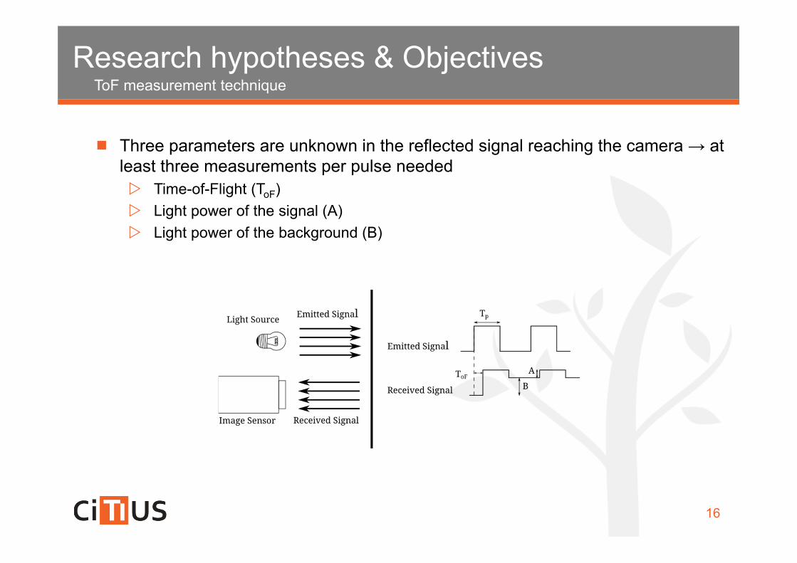
Three parameters are unknown in the reflected signal reaching the camera → at least three measurements per pulse needed Time-of-Flight (ToF) Light power of the signal (A) Light power of the background (B)

ToF measurement technique
Research hypotheses & Objectives
17
1
2
3
p p oF
p oF
p
x BT A T T
x BT AT
x BT
2 3
1 3 2 32 px xcL T
x x x x
ToF measurement technique
Research hypotheses & Objectives
18
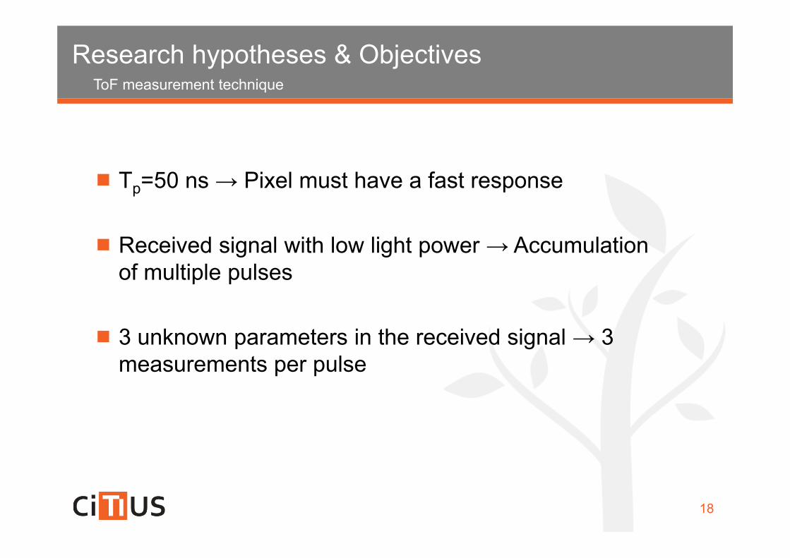
Tp=50 ns → Pixel must have a fast response
Received signal with low light power → Accumulation of multiple pulses
3 unknown parameters in the received signal → 3 measurements per pulse
Silicon photosensorsResearch hypotheses & Objectives
19
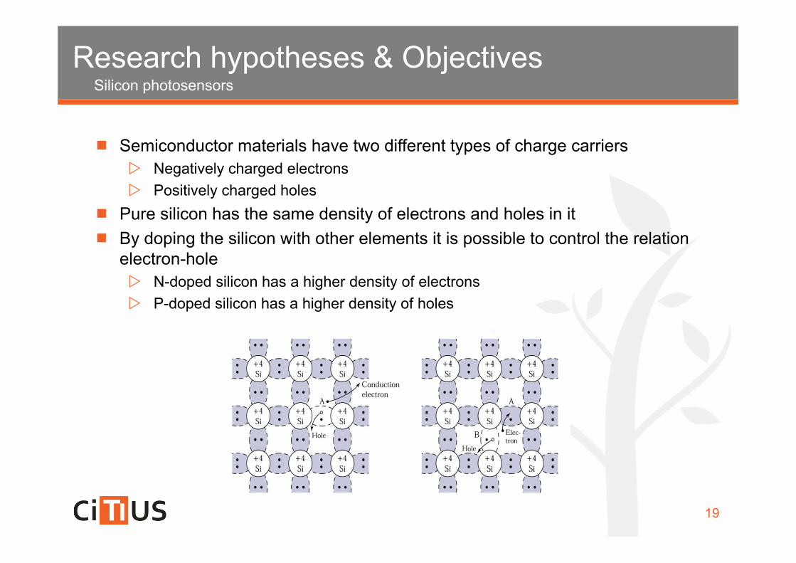
Semiconductor materials have two different types of charge carriers Negatively charged electrons Positively charged holes
Pure silicon has the same density of electrons and holes in it By doping the silicon with other elements it is possible to control the relation
electron-hole N-doped silicon has a higher density of electrons P-doped silicon has a higher density of holes
Silicon photosensorsResearch hypotheses & Objectives
20
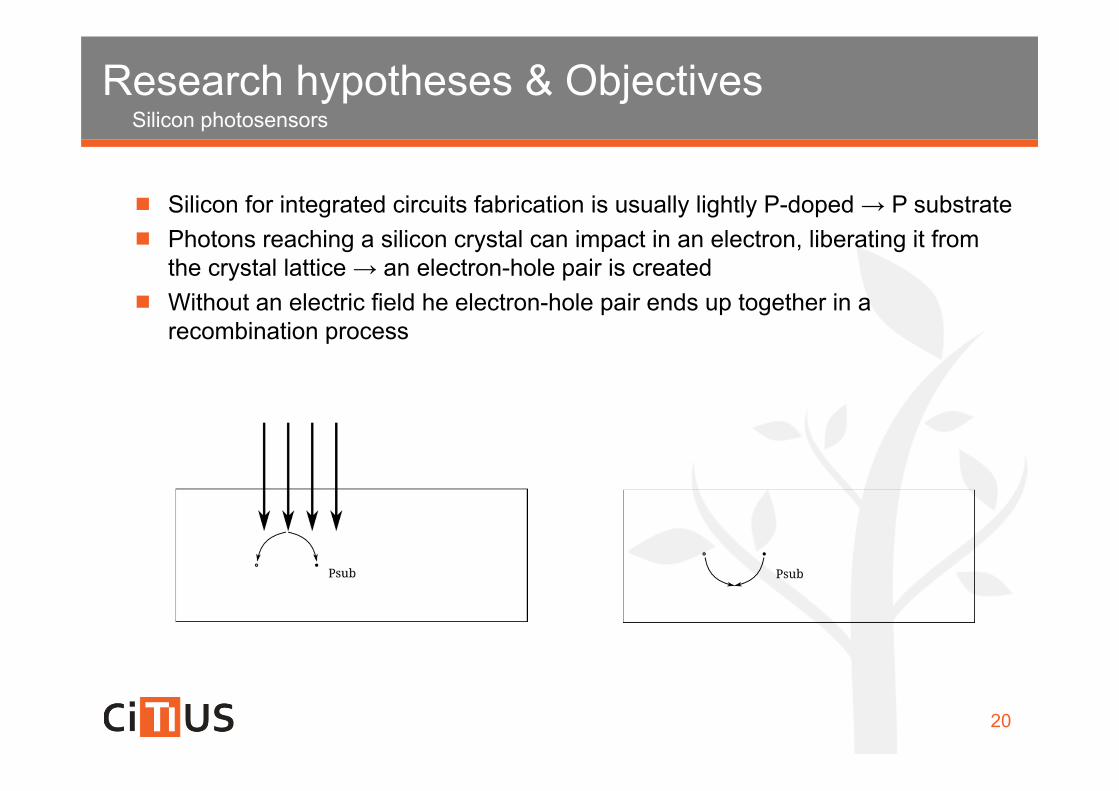
Silicon for integrated circuits fabrication is usually lightly P-doped → P substrate Photons reaching a silicon crystal can impact in an electron, liberating it from
the crystal lattice → an electron-hole pair is created Without an electric field he electron-hole pair ends up together in a
recombination process
Silicon photosensorsResearch hypotheses & Objectives
21
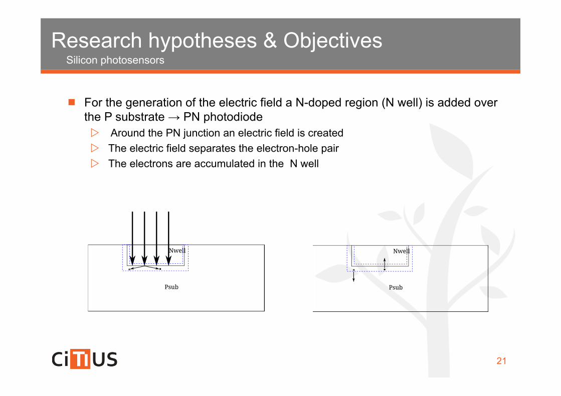
For the generation of the electric field a N-doped region (N well) is added over the P substrate → PN photodiode Around the PN junction an electric field is created The electric field separates the electron-hole pair The electrons are accumulated in the N well
3T pixelResearch hypotheses & Objectives
22
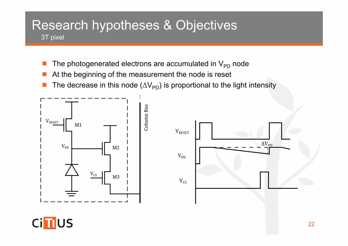
The photogenerated electrons are accumulated in VPD node At the beginning of the measurement the node is reset The decrease in this node (ΔVPD) is proportional to the light intensity
3T pixelResearch hypotheses & Objectives
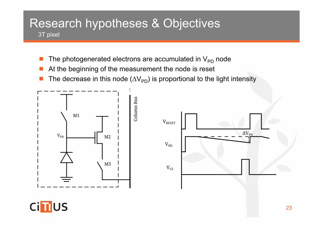
23
The photogenerated electrons are accumulated in VPD node At the beginning of the measurement the node is reset The decrease in this node (ΔVPD) is proportional to the light intensity
3T pixelResearch hypotheses & Objectives
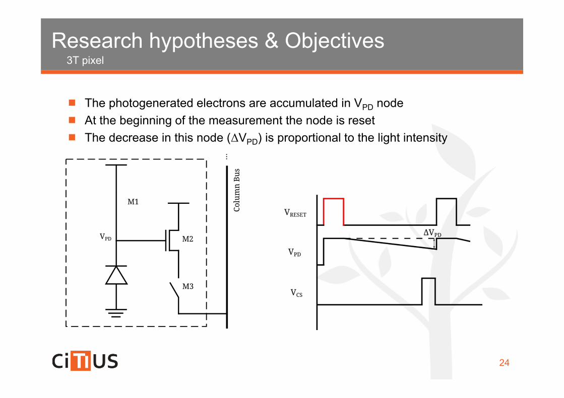
24
The photogenerated electrons are accumulated in VPD node At the beginning of the measurement the node is reset The decrease in this node (ΔVPD) is proportional to the light intensity
3T pixelResearch hypotheses & Objectives
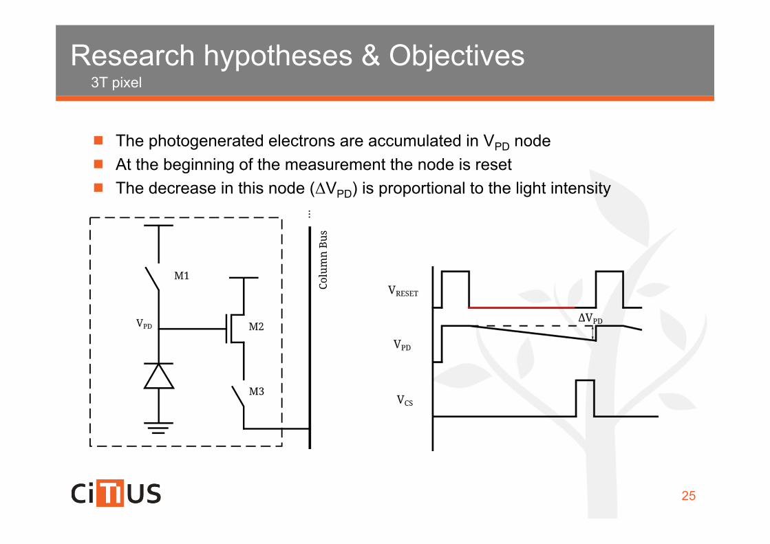
25
The photogenerated electrons are accumulated in VPD node At the beginning of the measurement the node is reset The decrease in this node (ΔVPD) is proportional to the light intensity

3T pixelResearch hypotheses & Objectives
26
The photogenerated electrons are accumulated in VPD node At the beginning of the measurement the node is reset The decrease in this node (ΔVPD) is proportional to the light intensity
3T pixelResearch hypotheses & Objectives
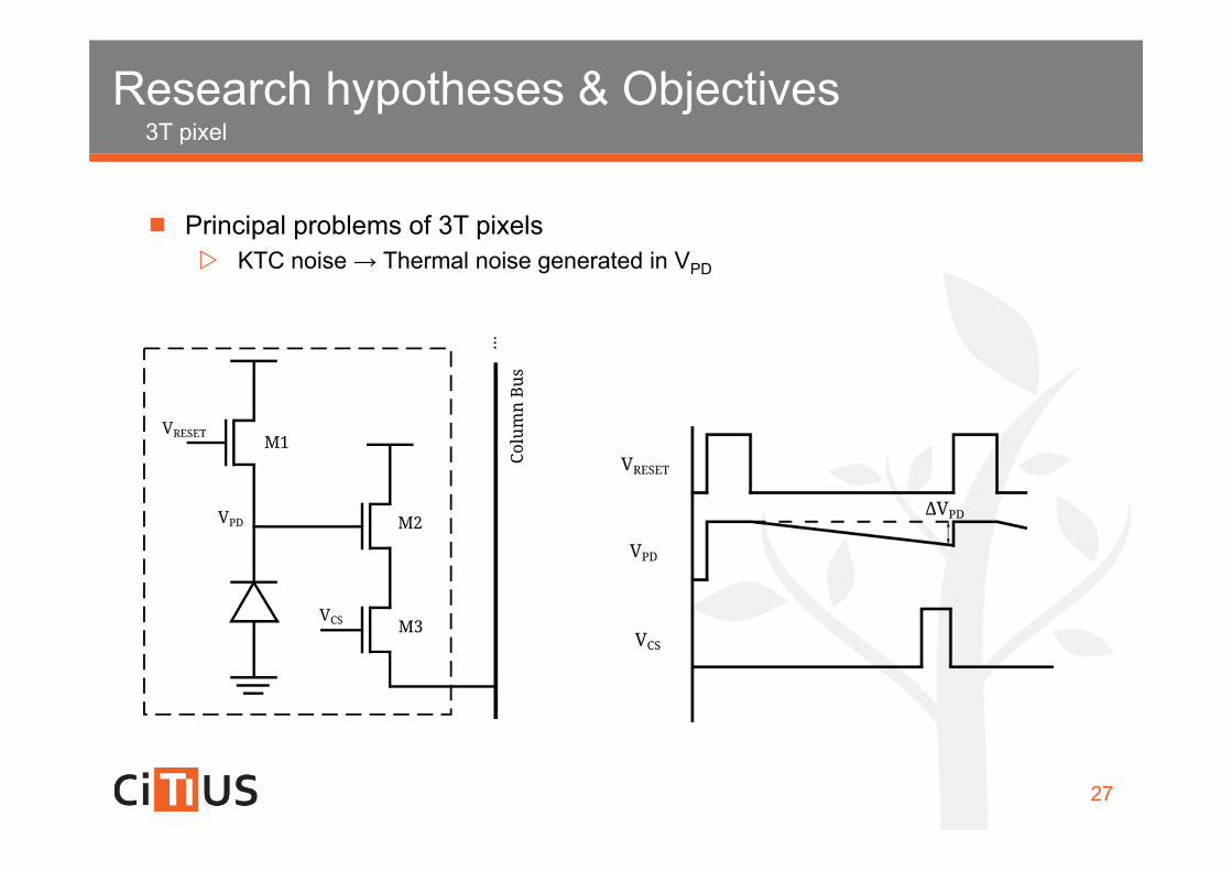
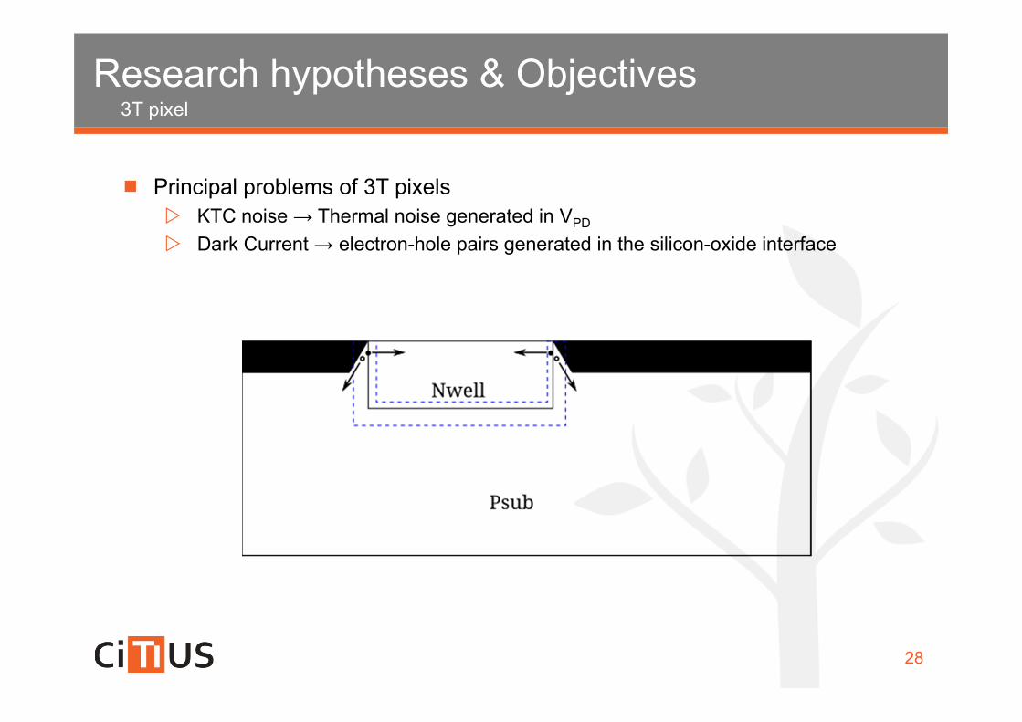
27
Principal problems of 3T pixels KTC noise → Thermal noise generated in VPD
3T pixelResearch hypotheses & Objectives
28
Principal problems of 3T pixels KTC noise → Thermal noise generated in VPD
Dark Current → electron-hole pairs generated in the silicon-oxide interface
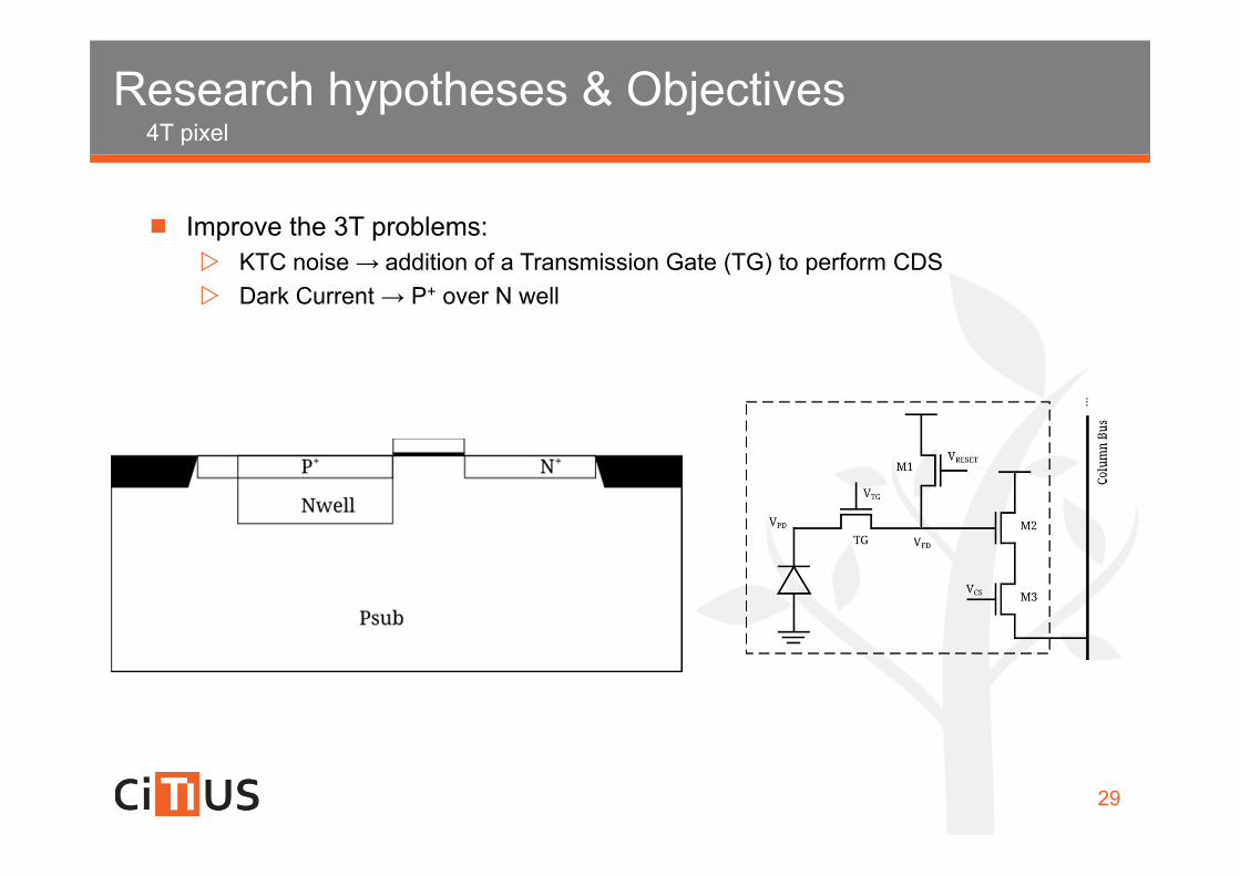
4T pixelResearch hypotheses & Objectives
29
Improve the 3T problems: KTC noise → addition of a Transmission Gate (TG) to perform CDS Dark Current → P+ over N well
4T pixelResearch hypotheses & Objectives
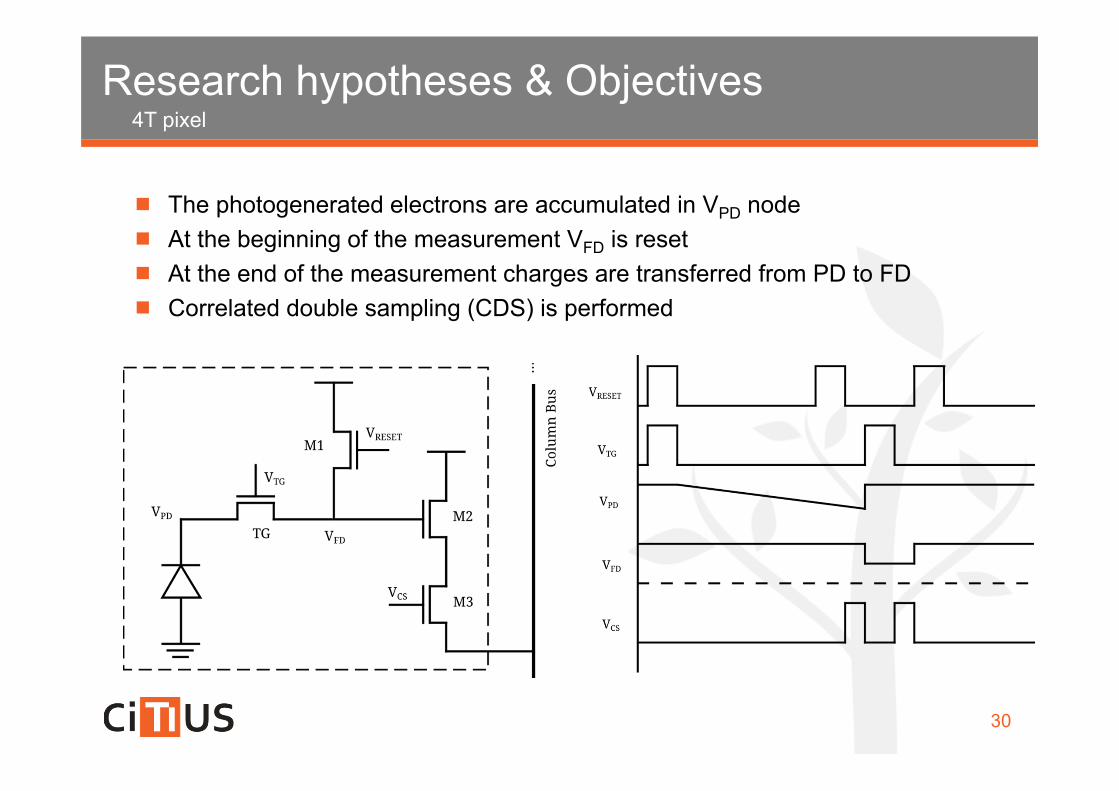
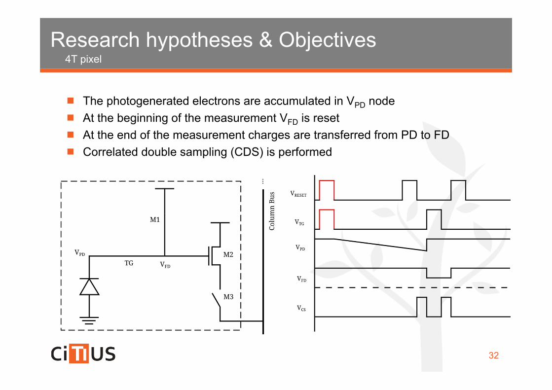
30
The photogenerated electrons are accumulated in VPD node At the beginning of the measurement VFD is reset At the end of the measurement charges are transferred from PD to FD Correlated double sampling (CDS) is performed

4T pixelResearch hypotheses & Objectives
31
The photogenerated electrons are accumulated in VPD node At the beginning of the measurement VFD is reset At the end of the measurement charges are transferred from PD to FD Correlated double sampling (CDS) is performed
4T pixelResearch hypotheses & Objectives
32
The photogenerated electrons are accumulated in VPD node At the beginning of the measurement VFD is reset At the end of the measurement charges are transferred from PD to FD Correlated double sampling (CDS) is performed
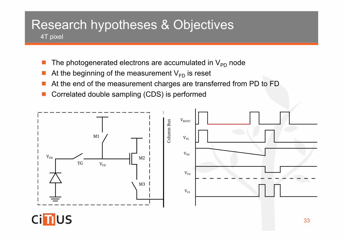
4T pixelResearch hypotheses & Objectives
33
The photogenerated electrons are accumulated in VPD node At the beginning of the measurement VFD is reset At the end of the measurement charges are transferred from PD to FD Correlated double sampling (CDS) is performed
4T pixelResearch hypotheses & Objectives
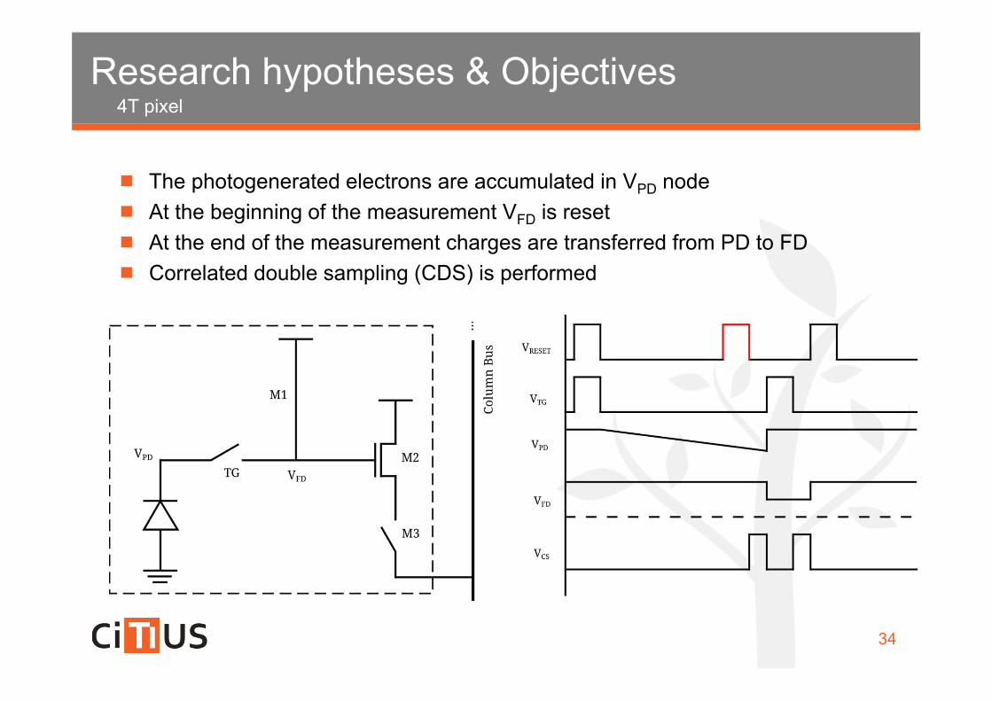
34
The photogenerated electrons are accumulated in VPD node At the beginning of the measurement VFD is reset At the end of the measurement charges are transferred from PD to FD Correlated double sampling (CDS) is performed
4T pixelResearch hypotheses & Objectives
35
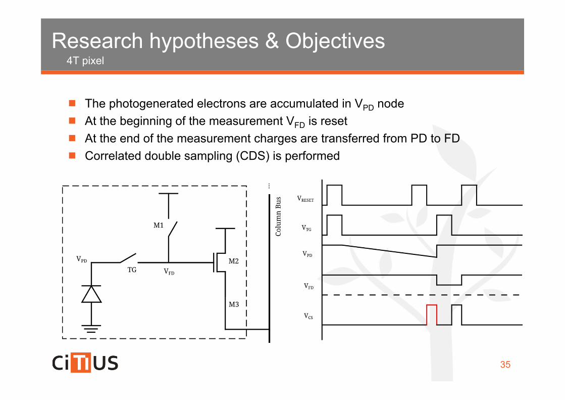
The photogenerated electrons are accumulated in VPD node At the beginning of the measurement VFD is reset At the end of the measurement charges are transferred from PD to FD Correlated double sampling (CDS) is performed
4T pixelResearch hypotheses & Objectives
36
The photogenerated electrons are accumulated in VPD node At the beginning of the measurement VFD is reset At the end of the measurement charges are transferred from PD to FD Correlated double sampling (CDS) is performed
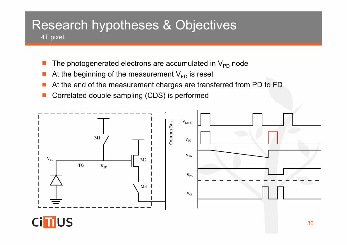
4T pixelResearch hypotheses & Objectives
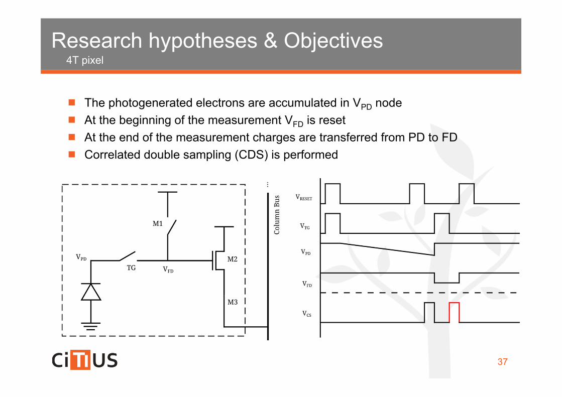
37
The photogenerated electrons are accumulated in VPD node At the beginning of the measurement VFD is reset At the end of the measurement charges are transferred from PD to FD Correlated double sampling (CDS) is performed
4T pixel for ToF
Research hypotheses & Objectives
38
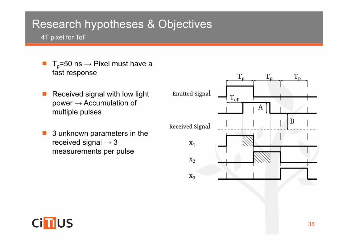
Tp=50 ns → Pixel must have a fast response
Received signal with low light power → Accumulation of multiple pulses
3 unknown parameters in the received signal → 3 measurements per pulse
4T pixel for ToFResearch hypotheses & Objectives
39
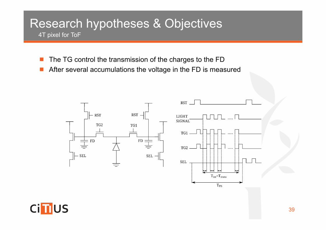
The TG control the transmission of the charges to the FD After several accumulations the voltage in the FD is measured
4T pixel in standard CMOS technologyResearch hypotheses & Objectives
40
Commercial PPD need a careful control of the doping concentrations Standard CMOS Technologies do not provide PPD 4T structures Design of P+ over Nwell with TG can be done violating layout rules To ensure correct behavior → Simulations with device-level simulator
(ATLAS from Silvaco) 2-D simulations Parameters needed
Doping profiles Horizontal Parameters Vertical Parameters
4T pixel in standard CMOS technology
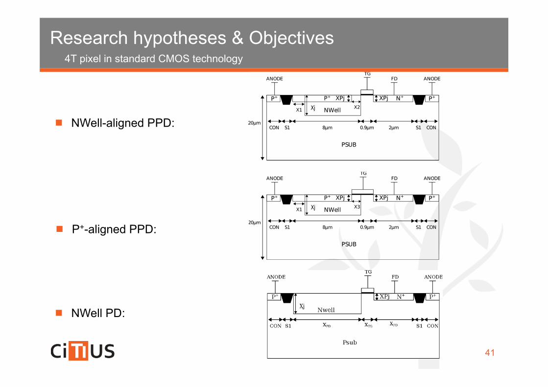
Research hypotheses & Objectives
41
NWell-aligned PPD:
P+-aligned PPD:
NWell PD:
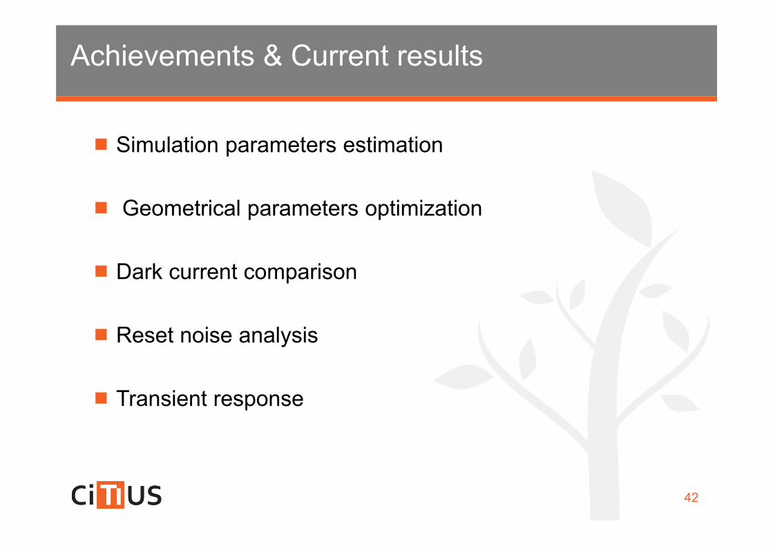
Achievements & Current results
42
Simulation parameters estimation
Geometrical parameters optimization
Dark current comparison
Reset noise analysis
Transient response
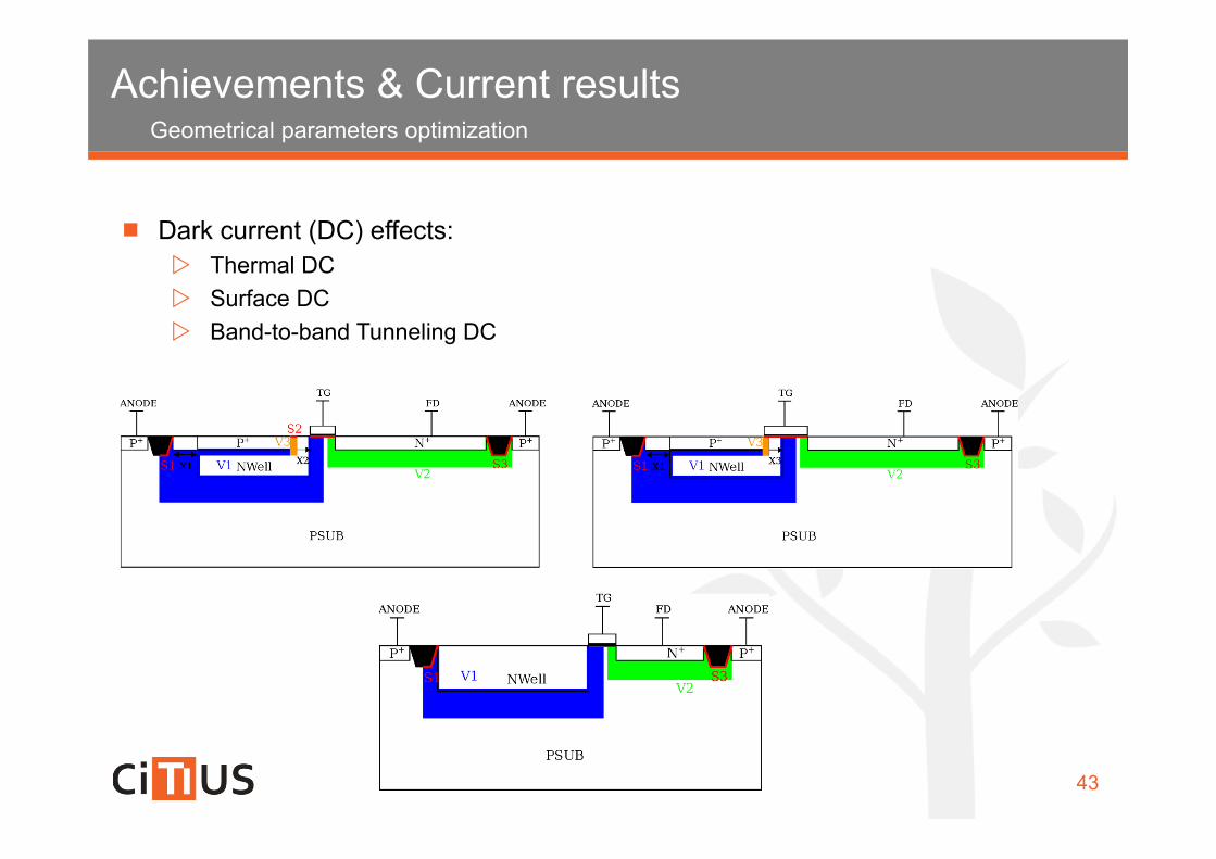
Geometrical parameters optimization
Achievements & Current results
43
Dark current (DC) effects: Thermal DC Surface DC Band-to-band Tunneling DC
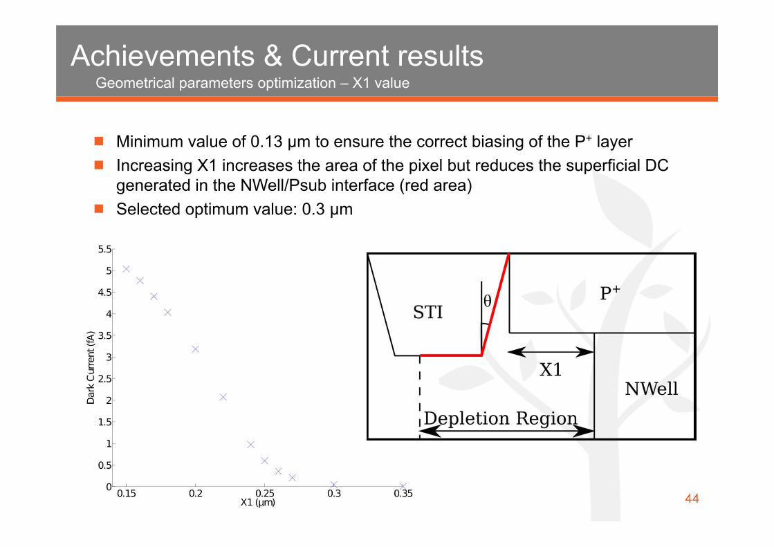
Geometrical parameters optimization – X1 valueAchievements & Current results
44
Minimum value of 0.13 μm to ensure the correct biasing of the P+ layer Increasing X1 increases the area of the pixel but reduces the superficial DC
generated in the NWell/Psub interface (red area) Selected optimum value: 0.3 μm
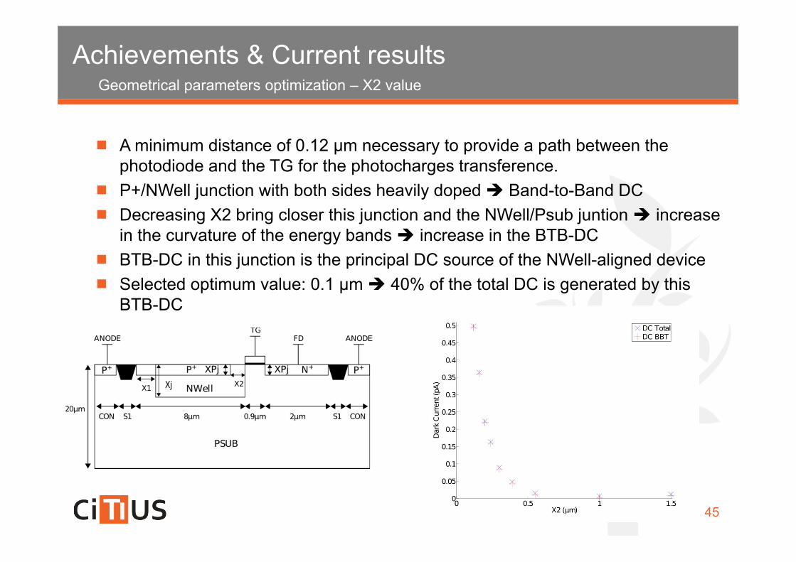
Geometrical parameters optimization – X2 value
Achievements & Current results
45
A minimum distance of 0.12 μm necessary to provide a path between the photodiode and the TG for the photocharges transference.
P+/NWell junction with both sides heavily doped Band-to-Band DC Decreasing X2 bring closer this junction and the NWell/Psub juntion increase
in the curvature of the energy bands increase in the BTB-DC BTB-DC in this junction is the principal DC source of the NWell-aligned device Selected optimum value: 0.1 μm 40% of the total DC is generated by this
BTB-DC
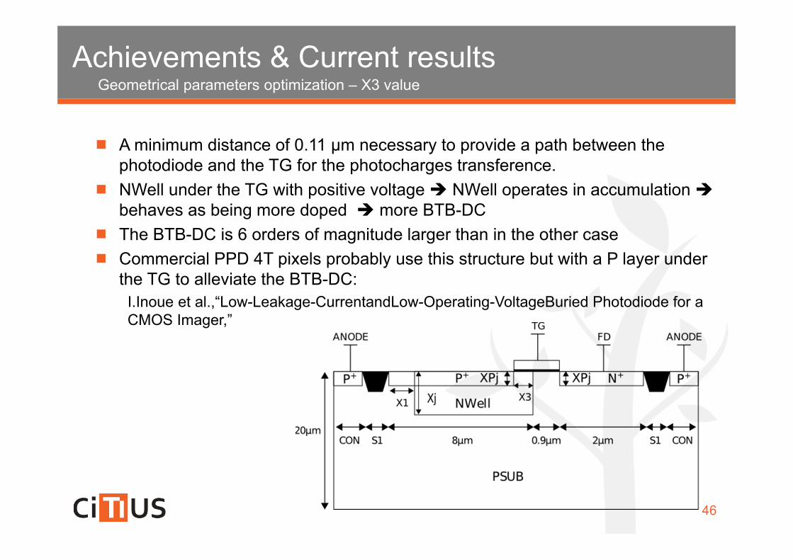
Geometrical parameters optimization – X3 valueAchievements & Current results
46
A minimum distance of 0.11 μm necessary to provide a path between the photodiode and the TG for the photocharges transference.
NWell under the TG with positive voltage NWell operates in accumulationbehaves as being more doped more BTB-DC
The BTB-DC is 6 orders of magnitude larger than in the other case Commercial PPD 4T pixels probably use this structure but with a P layer under
the TG to alleviate the BTB-DC: I.Inoue et al.,“Low-Leakage-CurrentandLow-Operating-VoltageBuried Photodiode for a CMOS Imager,”
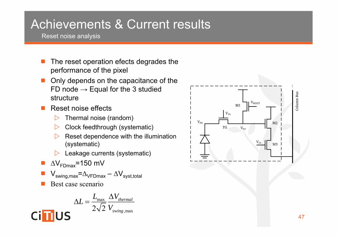
Reset noise analysisAchievements & Current results
47
The reset operation efects degrades the performance of the pixel
Only depends on the capacitance of the FD node → Equal for the 3 studied structure
Reset noise effects Thermal noise (random) Clock feedthrough (systematic) Reset dependence with the illumination
(systematic) Leakage currents (systematic)
ΔVFDmax=150 mV Vswing,max=ΔVFDmax – ΔVsyst,total
Best case scenario
max
,max2 2thermal
swing
L VLV
Reset noise analysisAchievements & Current results
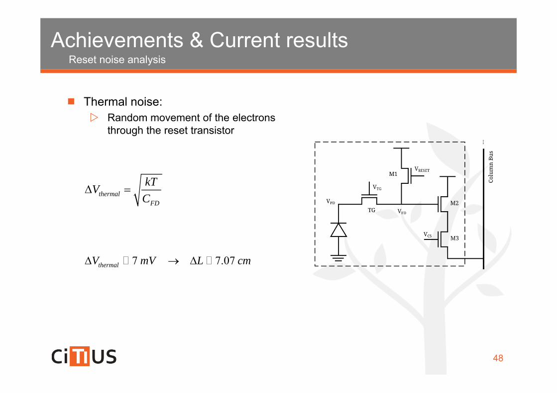
48
Thermal noise: Random movement of the electrons
through the reset transistor
thermalFD
kTVC
7 7.07thermalV mV L cm
Reset noise analysisAchievements & Current results
49
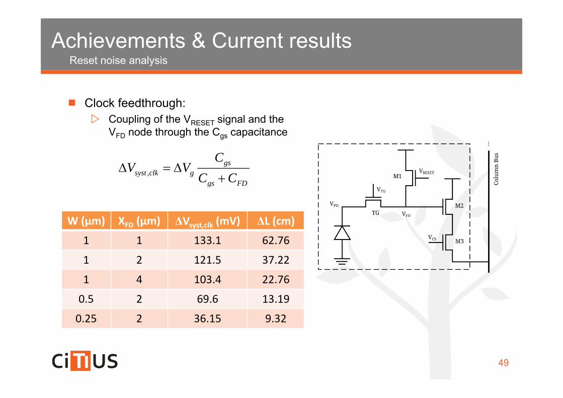
Clock feedthrough: Coupling of the VRESET signal and the
VFD node through the Cgs capacitance
,gs
syst clk ggs FD
CV V
C C
W (µm) XFD (µm) ΔVsyst,clk (mV) ΔL (cm)
1 1 133.1 62.76
1 2 121.5 37.22
1 4 103.4 22.76
0.5 2 69.6 13.19
0.25 2 36.15 9.32
Reset noise analysisAchievements & Current results
50
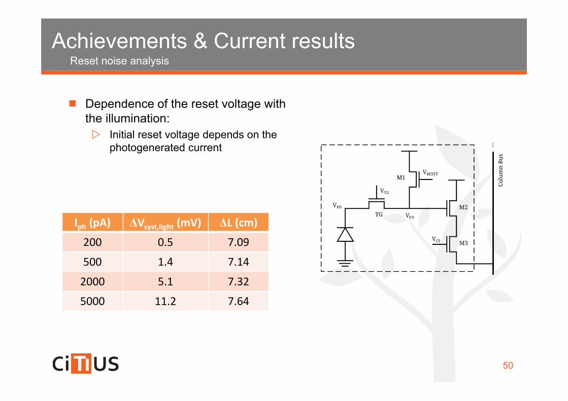
Dependence of the reset voltage with the illumination: Initial reset voltage depends on the
photogenerated current
Iph (pA) ΔVsyst,light (mV) ΔL (cm)
200 0.5 7.09
500 1.4 7.14
2000 5.1 7.32
5000 11.2 7.64

Reset noise analysisAchievements & Current results
51
Leakage current: Through the reset transistor flows
some current even being cut off
, 10 7.57syst leakageV mV L cm
Transient analysisAchievements & Current results
52
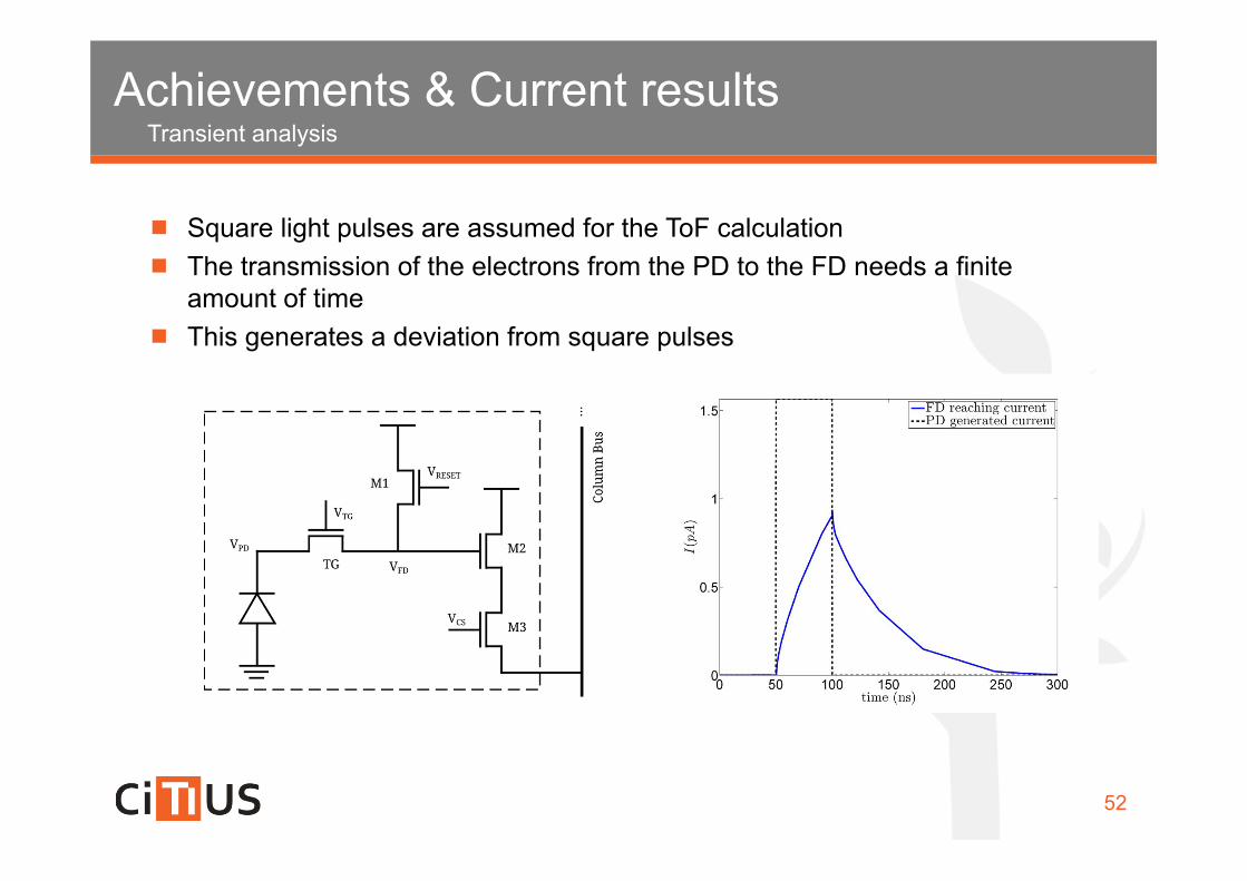
Square light pulses are assumed for the ToF calculation The transmission of the electrons from the PD to the FD needs a finite
amount of time This generates a deviation from square pulses

Transient analysisAchievements & Current results
53
NWell-aligned PPD:
NWell PD:
Transient analysisAchievements & Current results
54
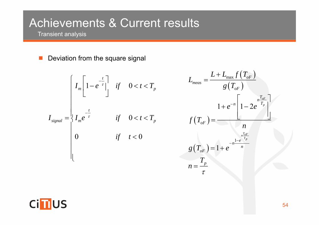
Deviation from the square signal
1 0
0
0 0
t
m p
t
signal m p
I e if t T
I I e if t T
if t
max
1
1 1 2
1
oF
p
ToFnTp
oFmeas
oF
TnTn
oF
enn
oF
p
L L f TL
g T
e e
f Tn
g T eT
n
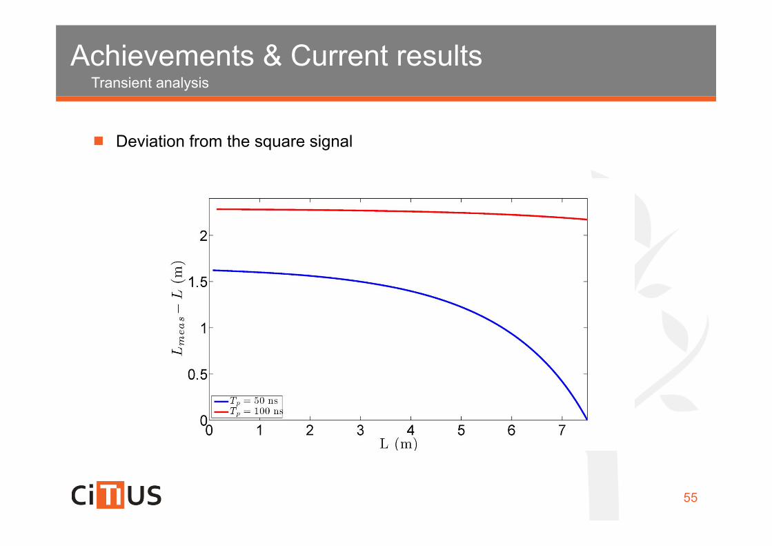
Transient analysisAchievements & Current results
55
Deviation from the square signal
PublicationsAchievements & Current results
56
Conferences: J. Illade-Quinteiro, V. Brea, P. López et al. “Comparison of Photosensing
Structures in CMOS Standard Technology for Time-of-Flight Sensors”, XXVIII Conference on Design of Circuits and Integrated Systems (DCIS), 2013, San Sebastián (Spain)
J. Illade-Quinteiro, V. Brea, P. López et al. "Dark current in standard CMOS pinned photodiodes for Time-of-Flight sensors," Microelectronics And Electron Devices (WMED), 2014 IEEE Workshop On , pp.1,4, 18-18 April 2014
J. Illade-Quinteiro, P. López, V. Brea et al. "Custom design of pinned photodiodes in standard CMOS technologies for time-of-flight sensors," Cellular Nanoscale Networks and their Applications (CNNA), 2014 14th International Workshop on , vol., no., pp.1,2, 29-31 July 2014
J. Illade-Quinteiro, P. López, V. Brea et al. “Dark Current Optimization of 4-Transistor Pixel Topologies in Standard CMOS Technologies for Time-of-Flight Sensors” , IEEE International Symposium on Circuits & Systems (ISCAS), 2015
PublicationsAchievements & Current results
57
Accepted publications: J. Illade-Quinteiro, P. López, V. Brea et al. “Four-Transistor Pinned Photodiodes
in Standard CMOS Technologies for Time-of-Flight Sensors”, Semiconductor Science and Technology Journal, 2015, Vol. 30, Num. 4, JCR (Q1)
J. Illade-Quinteiro, V. Brea, P. López et al. “Distance Measurement Error in Time-of-Flight Sensors Due to Shot Noise”, Sensors Journal JCR (Q1)
7 months of internship in Fondazione Bruno Kessler (FBK), Trento, Italy
This work has been partially funded by Spanish government projects TEC2009-12686 MICINN, TEC2012-38921-C02 MINECO (FEDER), Xuntade Galicia with EM2013/038, EM2014/012, AE CITIUS (CN2012/151, (FEDER)), GPC2013/040 (FEDER).
Future work
58
Design of an appropriate pixel for ToF in CMOS standard technology
Fabrication of the chip in 0.18 µm technology
Test of the chip
Defense of the thesis in the first trimester of 2016