(Solid-state biosensors and field-effect transistor ...
190
UNIVERSITY OF SÃO PAULO FFCLRP – DEPARTMENT OF PHYSICS GRADUATE IN PHYSICS APPLIED TO MEDICINE AND BIOLOGY Biossensores do estado sólido e dispositivos transistores de efeito de campo fabricados com semicondutores orgânicos (Solid-state biosensors and field-effect transistor devices based on organic semiconductors) HUGO JOSÉ NOGUEIRA PEDROZA DIAS MELLO Thesis submitted to the Faculty of Philosophy, Sciences and Letters of University of São Paulo, as part of the requirement for the degree of Doctor in Science. Area: Physics Applied to Medicine and Biology Ribeirão Preto – SP 2019
Transcript of (Solid-state biosensors and field-effect transistor ...

UNIVERSITY OF SÃO PAULO
FFCLRP – DEPARTMENT OF PHYSICS
GRADUATE IN PHYSICS APPLIED TO MEDICINE AND BIOLOGY
Biossensores do estado sólido e dispositivos transistores de
efeito de campo fabricados com semicondutores orgânicos
(Solid-state biosensors and field-effect transistor devices based on
organic semiconductors)
HUGO JOSÉ NOGUEIRA PEDROZA DIAS MELLO
Thesis submitted to the Faculty of
Philosophy, Sciences and Letters of
University of São Paulo, as part of the
requirement for the degree of Doctor in
Science. Area: Physics Applied to Medicine
and Biology
Ribeirão Preto – SP
2019

HUGO JOSÉ NOGUEIRA PEDROZA DIAS MELLO
Versão corrigida
Biossensores do estado sólido e dispositivos transistores de
efeito de campo fabricados com semicondutores orgânicos
Thesis submitted to the Faculty of
Philosophy, Sciences and Letters of
University of São Paulo, as part of the
requirement for the degree of Doctor in
Science.
Concentration area:
Physics Applied to Medicine and Biology
Supervisor:
Prof. Dr. Marcelo Mulato
Ribeirão Preto – SP
2019

I authorize the reproduction and total or partial disclosure of this work, by any
conventional or electronic means, for study and research purposes, as long as cited the
source.
FICHA CATALOGRÁFICA
Mello, Hugo José Nogueira Pedroza Dias Mello.
Biossensores do estado sólido e dispositivos transistores de efeito
de campo fabricados com semicondutores orgânicos / Hugo José Nogueira
Pedroza Dias Mello; Supervisor Marcelo Mulato. Ribeirão Preto – SP,
2019.
Thesis (PhD – Program of Postgraduate in Physics Applied to
Medicine and Biology) – Faculty of Philosophy, Sciences and Letters of
University of São Paulo. 2019.
1. Conducting polymers. 2. Organic electronic. 3. Bioreceptors. 4.
Sensors.

ii
Name: MELLO, Hugo José Nogueira Pedroza Dias Mello.
Title: Solid-state biosensors and field-effect transistor devices based on organic
semiconductors.
Thesis submitted to the Faculty of
Philosophy, Sciences and Letters of
University of São Paulo, as part of the
requirement for the degree of Doctor in
Science.
Approved in: ____ / ____ / ____
Examiners
Prof. Dr. : ____________________________ Institution: ________________________
Judgment: ____________________________ Signature: ________________________
Prof. Dr. : ____________________________ Institution: ________________________
Judgment: ____________________________ Signature: ________________________
Prof. Dr. : ____________________________ Institution: ________________________
Judgment: ____________________________ Signature: ________________________
Prof. Dr. : ____________________________ Institution: ________________________
Judgment: ____________________________ Signature: ________________________
Prof. Dr. : ____________________________ Institution: ________________________
Judgment: ____________________________ Signature: ________________________

iii
Dedicated to my beloved wife, Bianca B F D
Mello, who lived the dream with me, and to my
amazing family.

iv
Acknowledgment
I would like to express my sincere and eternal gratitude to those who made this
thesis possible.
I am deeply grateful to my supervisor Professor Marcelo Mulato, who supported
this work and encourage me to go beyond my own limits every second. His friendship
made the path easier.
I also express my gratitude to Professor Emil List-Kratochvil from Humboldt-
Universität zu Berlin for receiving me on his laboratory. His warm welcome along with
a dedicated guidance made my experience abroad enriching and fascinating, leading to
excellent results.
I would like to thank all my friends from the laboratory in Ribeirão Preto,
especially to those who warmly welcomed me in 2013, Tobias Heimfarth, Guilherme de
Oliveira Silva, Raphael Nascimento, Jessica Fernandes, Julio Ugucioni, Marina Batistuti,
and those who joined us, José Renato Alcarás, Bassam Junior, Ricardo Rocha, Luiz
Henrique Nunes, Fernando Mano, Stephanie Lisboa, Daísy Ferreira, Gustavo Madeira,
Lucas Matiola and Murilo Faleiros. Thank you for all the friendship along the years.
I would like also to thank Marcilio Mano Júnior, for all his support in the
laboratory, and Natalia Biziak (in memorian) for all her patience and help when I needed
the most.
From Humboldt University, I express my deep gratitude to Simon Dalgleish, who
guided me over the period I stayed in Berlin, trusted me and shared his knowledge. I
would like also to thank Felix Hermerschmidt, Giovanni Ligorio, Seon-Young Rhim,
Nicolas Zorn Morales, Sebastian Kickhöfel, Niklas Mutz, Max Heyl, Paul Hänsch, Minh

v
Hai Nguyen, Khoa Nguyen, Sebastian Pallasch, Edgar Nandayapa, Jeffrey Lyons, Bodo
Kranz and Paul Zybarth. They made the everyday life in Berlin extremely enjoyable.
I owe my deepest gratitude to my wife Bianca, my parents Ericson and Alda, my
stepmother Claudia and my stepfather Uziel, my brothers Igrayne, Yasmin and Yago, my
grandparents Alarico and Stella and my lovely family, in the name of Erica, Cassio,
Isabelle, Beatriz, Lavinia, Antonio, Maria, Sandra, Murilo, Osder, Silvana and Giovanna.
Words will never be enough to say thank you!
I would like to thank the University of São Paulo for providing me with an
excellent academic background and FAPESP for all financial support in Brazil
(2014/24559-0) and in Germany (2016/23305-0).
Thank you all!
vi
“Indeed, the only truly serious questions are ones that even
a child can formulate. Only the most naive of questions are
truly serious. They are the questions with no answers. A
question with no answer is a barrier that cannot be
breached. In other words, it is questions with no answers
that set the limit of human possibilities, describe the
boundaries of human existence.”
Milan Kundera
The Unbearable Lightness of Being

vii
Abstract
MELLO, H. J. N. P. D. Solid-state biosensors and field-effect transistor devices based
on organic semiconductors. 2019. Thesis (PhD – Program of Graduate in Physics
Applied to Medicine and Biology) – Faculty of Philosophy, Sciences and Letters of
University of São Paulo. Ribeirão Preto – SP, 2019.
Biosensors based on solid-state field-effect transistor as transducer stage using organic
semiconducting materials as sensing stage have been developed. Polyaniline thin films
galvanostatic electrodeposited were fabricated. Varied electrodeposition parameters were
tested, such as deposited charge, current density, deposition time and monomer
concentration, besides the tests of a polymeric blend composed of polyaniline and
polypyrrole and tested as pH potentiometric extended gate field-effect transistor sensor.
Then, biosensors were produced using the one-step electrochemical immobilization
process to obtain thin polyaniline films with entrapped glucose oxidase and urease
enzymes, to detection of glucose and urea, respectively. The optimized films presented
sensitivity, linearity and detection range to glucose of 14.6 ± 0.4 mV/decade, 99.8 % and
from 10-4 mol/L to 10-1 mol/L. Two different biosensors were produced based on the
enzymatic catalysis of urea with selectivity to ammonium or hydroxyl ions. For
ammonium ion selective films, the sensor presented sensitivity, linearity and detection
range of 14.7 ± 0.9 mV/decade, 98.2 % and from 10-5 mol/L to 10-1 mol/L. For the
hydroxyl ion selective film, the same parameters were 7.4 ± 0.5 mV/decade, 98.1 % and
from 10-5 mol/L to 10-1 mol/L. The same functionalized polyaniline thin films were used
in optical and conductometric biosensors due to the polyelectrochromic characteristic of

viii
the material. Improvement of the field-effect system was possible with the multimodal
array of enzymatic biosensor. The device was built using different enzymatic sensing
stages connected to the extended gate field effect transistor. The system decreased the
time needed to make distinct measurements, showed good response to the variation in
solution’s pH, to the presence of the reference film and to injection of target analyte in
solution in real time measurement. The electrolyte gated organic field-effect transistor
based on a polythiophene organic semiconducting layer was developed. A modular
enzymatic biosensor for glucose and urea, with a linear response in the range between 10-
6 and 10-3 mol/L, was achieved. This biosensor relies on the immobilization the enzymes
on gold rods, used as gate electrodes in the devices. The use of the bioreceptors proved
to be selective and cross-selective in the devices. The possibility of exchanging the
modified gate electrode to detect specific analytes using the same device system allows
the modular sensor to be reused and applied for a broad range of applications. Which is
the case for explosives molecules, TNT and DNT, biosensor fabricated in the same terms.
This biosensor relies on the immobilization of specific binding peptides for TNT and
DNT on the gold rod.
Key-words: 1. Conducting polymers. 2. Organic electronic. 3. Bioreceptors. 4. Sensors.

ix
List of figures
Figure 2.1 – Schematic illustration of a double bonded pair of carbon atoms in an ethylene
molecule in (a) and for polyacetylene in (b)..................................................................... 6
Figure 2.2 – Scheme of the MOSFET structure with its regions highlighted. ............... 11
Figure 2.3 – Energy band diagram for the MOSFET. EC is the energy of the conduction
band, Ei intrinsic energy level, EF Fermi level and EV is the valence band. .................. 12
Figure 2.4 – Simplified scheme of an ISFET based on a MOSFET. ............................. 14
Figure 2.5 – Schematic representation of an EGFET in which the chemically sensing
material is connected to the gate of a MOSFET. ............................................................ 16
Figure 2.6 – Three-dimensional illustration of an organic thin film transistor. ............. 18
Figure 2.7 – Scheme of an Electrolyte Gated Field-Effect Transistor (EGOFET) device.
........................................................................................................................................ 22
Figure 2.8 – Schematic operation of a sensor with several excitation sources. ............. 23
Figure 3.1 – Experimental setup for the Instrumental Amplifier EGFET (IA-EGFET)
system using the CA3140 Op-Amp with unity gain ...................................................... 35
Figure 3.2 – Chronopotentiometric curves for PANI deposition on FTO substrate at
various current densities in (a). Visible reflectance spectra of the PANI thin films in (b).
........................................................................................................................................ 38
Figure 3.3 – Measured thickness of the PANI thin films in (a), deposition efficiency of
the galvanostatic polymerization in (b), and the optical parameters lightness (L*) and
integrated reflectance in (c). ........................................................................................... 40
Figure 3.4 – SEM images for PANI thin films galvanostatic deposited. All the samples
have 300 mC cm-2 of deposited charge. The micrographs were enlarged 10000 times. In

x
(a) the PANI thin film sample J5T300, while in (b) the PANI thin film sample J10T300.
........................................................................................................................................ 42
Figure 3.5 – Potentiometric and optical sensor response of the PANI thin films. (a) the
IA-EGFET time response for sample J5T600. The inset is the IA-EGFET sensor structure.
(b) the response spectra of the optical sensor using sample J5T600. The marked rectangle
is the spectral green region. ............................................................................................ 44
Figure 3.6 – Sensor sensitivity and linearity are shown according to the total deposited
charge. Response for the IA-EGFET sensor in (a) and (b), and for the optical sensor in
(c) and (d). ...................................................................................................................... 45
Figure 3.7 – Illustration of PANI protonation process. In contact with protonic acid,
occurs the protonation in the quinoid rings, which have high affinity for charges. This
change can be detected by potentiometric and optical measurements and used as sensor
when measured as function of pH variation. .................................................................. 47
Figure 3.8 – Colour scale optical sensor sensitivity and linearity accordingly to the total
deposited charge for three parameters: L, a* and b*. For the set of films deposited with
current density 1.0 mA cm-2 in (a) and (b) and current density 0.5 mA cm-2 in (c) and (d).
........................................................................................................................................ 48
Figure 3.9 – In (a), chronopotentiometric curves for galvanostatic deposited PANI thin
films on FTO substrate at various aniline concentrations. The inset shows the variation of
the induction time of the PANI films according to the aniline concentration. In (b), visible
reflectance spectra of the galvanostatic deposited PANI thin films. Sample PANI20
presents variations in the spectral response. ................................................................... 51
Figure 3.10 – Measured thickness of PANI thin films in (a), the optical parameters
lightness (L*) and integrated reflectance in (b) and the theoretical model for the

xi
deposition efficiency and deposition rate for the galvanostatic deposited PANI thin films
in (c) as a function of aniline concentration. .................................................................. 53
Figure 3.11 – IA-EGFET sensor sensitivity (left y-axis) and linearity (right y-axis) are
shown accordingly to the aniline monomer concentration. In the far-right y-axis it is
shown the electrodeposition efficiency curve, which is clearly over the sensitivity
variation. ......................................................................................................................... 55
Figure 3.12 – SEM images for PANI thin films galvanostatic deposited varying the aniline
monomer concentration. Samples PANI10, PANI15, PANI20 and PANI25 are shown in
(a), (b), (c) and (d), respectively. .................................................................................... 57
Figure 3.13 – Chronopotentiometric curves of the PANI, 50/50 PANI/PPY and PPY
samples in (a). These curves are representative of the others composite samples, which
lie in between these, depending on the relative monomer proportion. Normalized
reflectance spectra for all thin films of the copolymer PANI/PPY in (b). The relative
intensity varies from the PANI to the PPY sample accordingly to the relative monomer
concentration. ................................................................................................................. 59
Figure 3.14 – Optical parameters integrated reflectance and brightness (L*) of the
PANI/PPY composite thin films in (a). The response is related to the thickness of the
samples and its composition. Colour parameter a* of the PANI/PPY composite film in
(b). Its variation is sensitive to the composition. The thickness of the samples is shown in
(c). The deposition efficiency is improved in cases where pyrrole predominates ......... 61
Figure 3.15 – SEM images for PANI/PPY composite thin films galvanostatic
electrodeposited. Images were enlarged 10,000 times. Micrographs of the FTO substrate
in (a), PANI homopolymer in (b), PANI/PPY composite in the proportion 50/50 in (c),
and PPY homopolymer in (d). ........................................................................................ 63

xii
Figure 3.16 – Response of PANI/PPY composite thin films as IA-EGFET chemical
sensors. The calibration curves of the PANI and PPY homopolymers and for the
PANI/PPY composite in the proportion 50/50 are shown in (a) together with the IA-
EGFET sensor structure in the inset. The behavior of the sensitivity and linearity for the
films is shown in (b). ...................................................................................................... 64
Figure 3.17 – Comparison between the chemical sensor sensitivity of the PANI/PPY
composite thin films and the optical integrated reflectance parameter. ......................... 66
Figure 4.1 – Sequence of events showed as a diagram for use of MAEB-D-IA-EGFET:
microcontroller determines the information transfer order of the multiplexer which in turn
performs readings of the input ports and connects them to the EGFET transducer. ...... 75
Figure 4.2 – The chronopotentiometric curves for GOx/PANI and Ur/PANI biosensors in
(a) and (b), respectively, showing no main differences between the samples. ............... 76
Figure 4.3 – The SEM morphology images for PANI, GOx/PANI and Ur/PANI thin films
prepared under the same experimental conditions are shown in (a), (b) and (c),
respectively. .................................................................................................................... 77
Figure 4.4 – Analysis of the optimal electrodeposition conditions and optimum pH for
bio-sensing of glucose and urea. The functionalized PANI thin films for the biosensor
obtained with the optimal parameters, as well as the optimal pH range. ....................... 78
Figure 4.5 – The EIS Nyquist diagram for GOx/PANI, Ur/PANI and the PANI samples
without enzymes for both biosensors. The inset shows more detailed graphs for the high
frequencies’ region. ........................................................................................................ 80
Figure 4.6 – Analysis of potentiometric EnFET biosensor. The calibration curve with the
sensitivity and linearity parameters for the GOx/PANI, Ur/PANI (NH4) and Ur/PANI
(OH) biosensors. ............................................................................................................. 81

xiii
Figure 4.7 – The stability, evolution over five weeks, and repeatability, evolution over
five consecutive experiments, of the sensitivity and linearity (in the inset), of the
GOx/PANI biosensors in (a), of Ur/PANI (OH) in (b) and of Ur/PANI (NH4) in (c). . 83
Figure 4.8 – Evolution of calibration curve for the Ur/PANI (NH4) biosensor over five
weeks. The curve changes its character from ascending to descending with increasing
concentration of urea in the solution. ............................................................................. 85
Figure 4.9 – Analysis of the oxidation states of PANI by means of reflectance
spectroscopy to determine the selectivity of the immobilization matrix. Reflectance
spectrum for four different samples: unfunctionalized PANI, GOx/PANI, Ur/PANI
(NH4) and Ur/PANI (OH) thin films in (a). Evaluation of the oxidation state variation
using the difference between the fifth- and first-week spectra of the films for GOx/PANI
and both Ur/PANI (NH4) and (OH) in (b). .................................................................... 87
Figure 4.10 – Spectral response curves as a function of the analyte concentration for the
glucose and urea biosensors, and their calibration curves. The spectral response for the
GOx/PANI biosensor in (a) and the spectral response for the Ur/PANI biosensor in (b).
The inset in both graphs shows the a* CIE colour parameter. The calibration curve and
indication of the sensitivity and linearity from GOx/PANI and Ur/PANI biosensors in (c).
........................................................................................................................................ 90
Figure 4.11 – The stability, evolution over five weeks, of the sensitivity and linearity of
GOx/PANI and Ur/PANI biosensors in (a). The stability of the a* CIE colour parameter
of GOx/PANI and Ur/PANI biosensors measured at concentration of 10-1 mol/L in (b)
and (c), respectively. ....................................................................................................... 93
Figure 4.12 – Raw data and fitted Nyquist diagram obtained by using the EIS technique.
EIS curves for the glucose GOx/PANI and urea Ur/PANI conductometric biosensors in
(a) and (b), respectively. ................................................................................................. 95

xiv
Figure 4.13 – The simpler equivalent circuit applied to PANI based systems and used in
this work in (a). RS is the resistance of the solution, RF is the resistance of the film, the
resistance for charge transfer in the polymeric structure, and it is in parallel with the
double-layer capacitance, C, formed on the film surface. The calibration curves and
indication of the sensitivity and linearity from GOx/PANI and Ur/PANI biosensors in (b).
The calibration curves based on the variation of the double-layer capacitance C and
solution impedance RS, in the inset, for the GOx/PANI and Ur/PANI biosensors in (c)
and (d), respectively. ...................................................................................................... 97
Figure 4.14 – Measured data from the MAEB system with GOx/PANI, Ur/PANI, and pH
sensing PANI films, in two different pH buffer solution, 5.9 and 7.6. The three squares
were used to indicate, approximately, the sensor response level of each film in pH 5.9
...................................................................................................................................... 101
Figure 4.15 – Measured data from the MAEB (black circles) and D-MAEB (black open
circles) systems with the thin films of GOx/PANI, Ur/PANI and PANI in (a). The
calibration curve of the copolymer PANI/PPY-50/50 thin film in (b). The phosphate
buffer solution pH’s was 5.9. ....................................................................................... 102
Figure 4.16 – Measured data for the MAEB (black circles) and D-MAEB (black open
circles) systems with the thin films of GOx/PANI, Ur/PANI and PANI using a phosphate
buffer solution with pH 7.6. ......................................................................................... 103
Figure 4.17 – Response of the D-MAEB system composed of GOx/PANI and Ur / PANI
biosensors, and chemical pH sensor, the PANI thin film, to glucose injection in the
phosphate buffer solution pH 5.9 of measurement. ...................................................... 104
Figure 4.18 – Response of the D-MAEB system composed of GOx/PANI and Ur / PANI
biosensors, and chemical pH sensor, the PANI thin film, to urea injection in the phosphate
buffer solution pH 7.6 of measurement. ....................................................................... 105
xv
Figure 5.1 – The functionalization of the gate electrode of an EGOFET (showed in cross-
section in a), allows for the fabrication of biosensor for analytes such as urea or glucose.
In (b), from left to right the strategy for the enzyme immobilization onto carboxylate-
terminated SAMs on Au gate rod is shown. Starting with MUA-SAM linker, followed by
the addition of NHS and the water soluble carbodiimide EDC to the SAMs results in the
formation of an NHS ester. Reaction of enzyme side-chain lysine residues with the ester
results in the formation of an amide bond. ................................................................... 108
Figure 5.2 – P3HT-based EGOFET device characterization. In (a) the output
characteristics of three devices (L ~ 30 µm and W ~ 1 mm) gated via DI water with a Pt
gate wire. The gate voltage, VGS, varied from 0.1 to - 0.3 V in 0.1 V steps and the drain-
source voltage, VDS, was swept from 0.0 to - 0.5 V. Transfer and semilogarithmic transfer
curves of three devices in the linear, VDS = - 0.1 V in (b), and saturation, VDS = - 0.4 V in
(c), regimes. Semilogarithmic transfer curves of the source-drain currents in the left-axis
and source-gate current in the right-axis vs. gate voltage in (d), when different maximum
gate voltages were applied with fixed VDS = - 0.1 V.................................................... 113
Figure 5.3 – Spectroelectrochemical analysis of the P3HT film with applied voltage from
0.05 to 1.0 V. For each applied voltage the spectra of the sample were recorded to stablish
a relationship between them. ........................................................................................ 115
Figure 5.4 – A composite P3HT/PMMA (3:7 wt. ratio) - based EGOFET device
characterization. In (a) the output characteristics of one device (L ~ 30 µm and W ~ 1
mm) gated via DI water with a Pt gate wire. The gate voltage, VGS, varied from 0.1 to -
0.3 V in a 0.1 V step and the drain-source voltage, VDS, varied from 0 to - 0.5 V. Transfer
and semilogarithmic transfer curves of three devices in the linear, VDS = - 0.1 V in (b),
and saturation, VDS = - 0.4 V in (c), regime. Semilogarithmic transfer curves of the source-

xvi
drain currents in the left-axis and source-gate current in the right-axis vs. gate voltage in
(d), when different maximum gate voltages were applied with fixed VDS = - 0.1 V. .. 116
Figure 5.5 – Analysis of the ratio IDS/IDS(max) obtained from transfer curves of P3HT-
and P3HT/PMMA-based EGOFET gated via Pt wire in DI water applying a stable and
non-stable maximum gate voltage, VGS = - 0.3 and - 0.5 V, respectively, at four distances
positions between the EGOFET device and Pt gate wire, using a fixed VDS = - 0.1 V.
...................................................................................................................................... 119
Figure 5.6 – Transfer curves of P3HT transistors in the linear regime with three different
gate electrodes: The Au bare gate wire, the glucose-oxidase, GOx/Au, modified gate wire
and the urease, Ur/Au, modified gate wire in (a). Variation in the transfer curve in the
linear regime, VDS = - 0.1 V, for the glucose biosensor, GOx/Au, at glucose concentration
varying from 10-6 to 10-3 mol/L and for DI-water. ....................................................... 121
Figure 5.7 – Variation in the transfer curve in the linear regime, VDS = - 0.1 V, for the
urea biosensor, Ur/Au, at urea concentration varying from 10-6 to 10-3 mol/L and for DI-
water. ............................................................................................................................ 122
Figure 5.8 – In (a) the changing in the relative drain-source current (ΔIDS/IDS) of the
EGOFET device for the glucose biosensor, GOx/MUA/Au, at glucose concentration
varying from 10-6 to 10-1 mol/L in the linear regime, VDS = - 0.1 V, in a forward
measurement protocol. The same response for the EGOEFT device for the Au bare gate
rods also shown. In (b) the reversibility analysis of the EGOFET based glucose biosensor.
The first five experiments were done with pure water, then with glucose at 10-4 mol/L and
back to pure water until the device recovered it previous response level. ................... 123
Figure 5.9 – In (a) the changing in the relative drain-source current (ΔIDS/IDS) of the
EGOFET device for the urea biosensor, Ur/MUA/Au, at urea concentration varying from
10-6 to 10-1 mol/L in the linear regime, VDS = - 0.1 V, in a forward measurement protocol.

xvii
The same response for the EGOEFT device for the Au bare gate is also shown. In (b) the
reversibility analysis of the EGOFET based urea biosensor. The first five experiments
were done with pure water, then with urea at 10-4 mol/L and back to pure water for 4
times. ............................................................................................................................ 125
Figure 5.10 – Selectivity analysis of the EGOFET based enzyme modified biosensors
with relative drain-source (ΔIDS/IDS) of the device against glucose and urea analytes. The
Au bare gate rod electrode was measured for non-specific binding analysis. .............. 126
Figure 5.11 – Transfer curves of P3HT transistors in the linear regime with four different
gate electrodes: The Au bare gate wire, the TNT binding peptide, TNT-BP, the DNT
binding peptide, DNT-BP, and the scramble binding peptide, Scr-BP, modified gate wires
in (a). Variation in the transfer curve in the linear regime, VDS = - 0.1 V, for the TNT
biosensor, TNT-BP, at TNT concentration varying from 10-15 to 10-6 mol/L, showing
intercalated curves to a clear presentation in (b). ......................................................... 129
Figure 5.12 – The changing in the relative drain-source current (ΔIDS/IDS) of the EGOFET
device for the TNT biosensor, TNT-BP, at TNT concentration varying from 10-15 to 10-4
mol/L, in (a), and for the DNT biosensor, DNT-BP, at DNT concentration varying from
10-6 to 10-4 mol/L, in (b), in the linear regime, VDS = - 0.1 V, in a forward and back
measurement protocol................................................................................................... 131
Figure 5.13 – Selectivity analysis of the EGOFET based peptide modified biosensors with
relative drain-source current (ΔIDS/IDS) of the device against TNT and DNT analytes. The
bare Au and Scr-BP modified gate electrodes were measured for non-specific binding
analysis. ........................................................................................................................ 132

xviii
List of tables
Table 3.1 – Deposited charge of the PANI thin films. Current density and deposition time
for each film are shown. Sample identification is based on the current density and
deposition time. .............................................................................................................. 33
Table 3.2 – Electropolymerization solution monomer concentration for each relative
proportion. Aniline and pyrrole monomer concentration for each solution for the constant
final polymeric concentration of 0.25 mol/L. Sample identification is based on the relative
monomer concentration. ................................................................................................. 34
Table 4.1 – Detection characteristics of previously reported glucose and urea biosensors
with different immobilization matrix material and immobilization technique and of the
device reported in this thesis. ......................................................................................... 82

xix
List of abbreviation
MUA 11-Mercaptoundecanoic Acid
EDC 1-Ethyl-3-(3-Dimethylaminopropyl)
PFBT 2,3,4,5,6-Pentafluorobenzenethiol
TNT 2,4,6-Trinitrotoluene
σ* Antibonding Orbital
BP Binding Peptides
σ Bonding Orbital
L Channel Length
W Channel Width
RCT Charge Transfer Resistance
CV Cyclic Voltammetry
CIE Commission Internationael De l'Eclairage
CMOS Complementary Metal-Oxide-Semiconductor
j Current Density
DI Deionized Water
t Deposition Time
ø Diameter
D-IA-EGFET
Differential Instrumental Amplifier Extended Gate Field-Effect
Transistor
D-MAEB Differential Multimodal Array of Enzymatic Biosensor
DPV Differential Pulse Voltammetry
DNT Dinitrotoluene

xx
D Drain
IDS Drain-Source Current
VDS Drain-Source Voltage
EAP Electroactive Polymer
EIS Electrochemical Impedance Spectroscopy
ERGO Electrochemically Reduced Graphene Oxide
EGOFET Electrolyte Gated Organic Field-Effect Transistor
EnFET Enzymatic Field-Effect-Transistor
EDTA Ethylenediaminetetraacetic Acid
EGFET Extended Gate Field-Effect Transistor
F Faraday Constant
µ Field-Effect Mobility
FET Field-Effect Transistor
FTO Fluorine Doped Tin Oxide
G Gate
IGS Gate-Source Current
VGS Gate-Source Voltage
GOx Glucose Oxidase
HOMO Highest Occupied Molecular Orbital
HPLC High-Performance Liquid Chromatography
HCl Hydrochloric Acid
ITO Indium Tin Oxide
IA-EGFET Instrumental Amplifier-Egfet
IR Integrated Reflectance
ISFET Ion Sensitive Field-Effect Transistor

xxi
IPMC Ionic Polymer Metal Composite
ISFET Ion-Sensitive Field-Effect Transistor
L Linearity
LUMO Lowest Unoccupied Molecular Orbital
L* Luminance Scale
MIS Metal-Insulator-Semiconductor
MOSFET Metal-Oxide-Semiconductor Field-Effect Transistor
mV/pH Milivolts Per Ph
MW Molecular Weight
mol/L Moles Per Liter
MWCNT Multi Walled Carbon Nanotubes
MAEB Multimodal Array of Enzymatic Biosensor
NHS N-Hydroxysuccinimide
s Number of Electrons Transferred
OTS Octadecyltrichlorosilane
OFET Organic Field-Effect Transistor
OLED Organic Light Emitting Diode
OSC Organic Semiconducting
PBS Phosphate Buffer Solution
PEDOT/PSS Poly (3,4-Ethylendioxytiophene)-Poly (Styrene Sulfonate)
P3HT Poly(3-Hexylthiophene)
PMMA Poly (Methyl Methacrylate)
PANI Polyaniline
PANI-EB Polyaniline Emeraldine Base
PANI-ES Polyaniline Emeraldine Salt

xxii
PANI-LE Polyaniline Leucoemeraldine
PANI-PE Polyaniline Pernigraniline
PDA Polydiacetylene
PDMS Polydimethylsiloxane
PE Polyethylene
ρ Polymer Density
PT Polythiophene
KCl Potassium Chloride
PEMFC Proton Exchange Membrane Fuel Cells
RFID Radio-Frequency Identification
REFET Referential Field-Effect Transistor
rpm Rotations Per Minute
a* Scale Between Red and Green
b* Scale Between Yellow and Blue
SEM Scanning Electron Microscopy
S Sensitivity
SiO2 Silicon Oxide
Ag/AgCl Silver/Silver Chloride
S-EGFET Single-EGFET
S Source
SMU Source-Measure Unit
SPR Surface Plasmon Resonance
SERS Surface-Enhanced Raman Spectroscopy
THF Tetrahydrofuran
VTH Threshold Voltage

xxiii
TiO2 Titanium Dioxide
WHW Tryptophan-Histidine-Tryptophan
Ur Urease
xxiv
Contents
List of figures .................................................................................................................. ix
List of tables ................................................................................................................ xviii
List of abbreviation ........................................................................................................ xix
1. Introduction .............................................................................................................. 1
1.1. Aim of the thesis ................................................................................................ 2
1.2. Overview of the thesis ....................................................................................... 3
2. Theories and principles ............................................................................................. 5
2.1. Organic semiconductors .................................................................................... 5
2.1.1. Polyaniline .................................................................................................. 8
2.1.2. Poly(3-hexylthiophene) .............................................................................. 9
2.2. Field-effect transistors ..................................................................................... 10
2.2.1. Metal-oxide-semiconductor field-effect transistor (MOSFET) ................ 10
2.2.2. Ion sensitive Field-effect transistor (ISFET) ............................................ 13
2.2.3. Extended gate field-effect transistor (EGFET) ......................................... 15
2.2.5. Electrolyte Gated Field-Effect Transistor – EGOFET ............................. 21
2.3. Sensors ............................................................................................................. 22
2.3.1. Biosensors – definition, classification and types ...................................... 23
3. Fabrication and application of PANI thin film ....................................................... 27
3.1. Methodology .................................................................................................... 32
3.1.1. Materials ................................................................................................... 32

xxv
3.1.2. PANI and PANI/PPY thin film synthesis ................................................. 32
3.1.3. Sample characterization ............................................................................ 34
3.1.4. Sensor measurement ................................................................................. 35
3.2. Influence of current density and deposition time ............................................. 37
3.3. Influence of aniline monomer concentration ................................................... 50
3.4. PANI/PPY composite thin films ...................................................................... 58
4. Biosensors based on PANI thin film ...................................................................... 68
4.1. Methodology .................................................................................................... 71
4.1.1. Materials ................................................................................................... 71
4.1.2. Sample characterization ............................................................................ 72
4.1.3. Biosensors measurement .......................................................................... 73
4.2. PANI based EnFET biosensor ......................................................................... 75
4.2.1. Functionalized PANI characterization and optimization.......................... 75
4.2.2. EnFET biosensor measurement ................................................................ 80
4.2.3. Stability and repeatability analysis ........................................................... 83
4.2.4. Selectivity analysis ................................................................................... 86
4.2.5. Partial conclusion ..................................................................................... 88
4.3. PANI based optical and conductometric biosensor ......................................... 89
4.3.1. Analysis of optical biosensor .................................................................... 89
4.3.2. Stability of the optical biosensor .............................................................. 92
4.3.3. Analysis of conductometric biosensor ...................................................... 95
4.3.4. Partial conclusions .................................................................................... 99
4.4. Multimodal array of enzymatic biosensors (MAEB) .................................... 100

xxvi
4.4.1. pH effect on the MAEB .......................................................................... 100
4.4.2. REFET effect in the MAEB ................................................................... 101
4.4.3. Glucose and urea detection with MAEB ................................................ 104
4.4.4. Partial conclusions .................................................................................. 106
5. EGOFET based biosensor .................................................................................... 107
5.1. EGOFET based on P3HT .............................................................................. 111
5.1.1. Methodology ........................................................................................... 111
5.1.2. EGOFET evaluation ............................................................................... 112
5.2. P3HT based EGOFET enzymatic biosensor .................................................. 120
5.2.1. Sample preparation ................................................................................. 120
5.2.2. Biosensor evaluation .............................................................................. 120
5.3. P3HT based EGOFET TNT and DNT biosensor .......................................... 127
5.3.1. Sample preparation ................................................................................. 128
5.3.2. Biosensor evaluation .............................................................................. 128
6. Conclusions .......................................................................................................... 134
List of publication ......................................................................................................... 137
References .................................................................................................................... 138

Introduction Hugo José N. P. Dias Mello
1
1. Introduction
The biosensor research field has experienced explosive growth over the last three decades.
A biosensor is generally defined as an analytical device which converts a biological
response into a quantifiable and processable signal. They can be applied to a large variety
of samples including body fluids, food samples, cell cultures and be used to analyse
environmental samples.
One important contribution to the broad area of biosensors is the introduction of
the first-generation glucose oxidase (GOx) biosensor in 1962 [1]. The GOx biosensor is
still the most widely used, although many improvements (generations) have been added
since the 1960’s. As exemplified by the glucose biosensor, solid-state biosensors do not
suffer the drawback of high sensor setup complexity and cost. This is due to their close
link to developments in low-cost production of microelectronic circuits and their easy
interface with normal electronic read-out and processing. Other inherent advantages of
these biosensors are their robustness, easy miniaturization, excellent detection limits, and
small analyte volumes.
Among many examples, potentiometric solid-state biosensors have been widely
used and studied. The first ion-sensitive field-effect transistor (ISFET) potentiometric
sensor was fabricated by Bergveld [2]. The device was a chemical ion sensor based on
metal-oxide-semiconductor field effect transistor (MOSFET) technology. The
component had its metal gate removed in order to expose the underlying insulator layer
to the solution. This had the function of an ion selective electrode. The extended-gate
field effect transistor (EGFET) arose from a modification in the ISFET structure where
the sensing membrane was separately fabricated and connected to the transistor’s gate.

Introduction Hugo José N. P. Dias Mello
2
The development of more sophisticated materials and devices allowed more technological
and modern solid-state based biosensors.
Organic semiconducting materials, such as conducting polymers or molecules are
especially suitable for solid-state potentiometric biosensor development for providing
biomolecule immobilization and for rapid electron transfer. The possibility of biological
sensing elements entrapment in polymeric material is an interesting way to the
development of useful biosensor devices. The same class of materials gave rise to organic
field-effect transistors (OFETs) devices. The outstanding features of organic-based
devices, such as low temperature processability, low-cost fabrication, miniaturization and
integration on flexible substrates, has led to sensor assemblies for health-, food- and
environmental monitoring. The biocompatibility is also important when it comes to
biomedical applications and the envisioned human interfacing. For biosensors,
specifically, the electrolyte gated organic field-effect transistor (EGOFET) architecture,
which differs from an OFET by having the gate separated from the transistor’s channel
by an electrolyte, has shown much promise once its electrolyte can act as an analyte
medium where high sensitivity can be achieved as a result of analyte-induced changes to
the electrochemical potential across the dielectric.
1.1. Aim of the thesis
The aim of this thesis is to develop biosensor based on solid-state field-effect transistor
transducer with organic semiconducting material. Two kind of biosensors were
developed: enzymatic biosensors for the detection of glucose and urea, which are
important analytes for human health, and biosensor for explosive analytes detection, TNT
and DNT, which are important not only to human health but also to human safety. The
first biosensor was developed in two FET based device platforms, the first one is an
EGFET based biosensor using functionalized polyaniline (PANI) thin films as sensing

Introduction Hugo José N. P. Dias Mello
3
stage, and the second one an EGOFET based biosensor using functionalized gold rods
applied as gate electrode and poly(3-hexylthiophene) (P3HT) as the organic
semiconducting (OSC) layer. This last system device was the one used for the explosive
analytes biosensing, obtained by the functionalization of the gold rod gate electrodes by
specific binding peptides.
The first biosensor was developed at University of São Paulo, in the Faculty of
Philosophy, Sciences and Letter of Ribeirão Preto, under supervision of Prof. Marcelo
Mulato in the SENSORMAT research group laboratory, funded by FAPESP (Fundação
de Amparo à Pesquisa do Estado de São Paulo) Brazilian agency (2014/24559-0). The
second biosensor was developed at Humboldt University, Berlin, Germany, in the
Institute of Physic, Chemistry and IRIS Adlershof, under supervision of Prof. Emil List-
Kratchovil in the Hybrid Device group research laboratory, funded by FAPESP
(2016/23305-0).
1.2. Overview of the thesis
Chapter 2 introduces the basic theory and principles, starting with organic
semiconductors, PANI and P3HT, followed by field-effect transistors, describing the
historical evolution, from MOSFET, ISFET, EGFET, OFET to EGOFET, finishing with
the biosensor’s development.
Chapter 3 introduces the study on the fabrication and application of PANI thin
films in chemical sensors based on EGFET transducer system. It includes the synthesis
of the polymeric thin films, their characterization and application in the EGFET pH
sensor, focusing on analyses of electrodeposition parameters effect on the final device.
Solid-state field-effect transistor biosensor based on functionalized PANI thin
films is presented on chapter 4. The chapter describes the functionalization of PANI thin
film, the biosensor performance and the study of stability, repeatability and selectivity of
Introduction Hugo José N. P. Dias Mello
4
EnFET biosensor. The same functionalized PANI thin films are also applied to optical
and conductometric biosensors due to their polyelectrochromic characteristic. The last
section of the chapter presents the application of the functionalized PANI thin films for
simultaneous measurement of distinct target analytes from the same solution with a
multimodal array of enzymatic biosensor (MAEB) device.
EGOFET based biosensors to glucose, urea and explosive analytes is presented
on chapter 5. It includes the development of EGOFET devices based on P3HT OSC layers
before its utilization for the detection of glucose and urea. The last section describes the
TNT and DNT biosensor.
The final remarks are presented in Chapter 6 closing the scientific development
made in this thesis.

Theories and principles Hugo José N. P. Dias Mello
5
2. Theories and principles
2.1. Organic semiconductors
Organic materials are compounds based on carbon in combination with other elements
such as hydrogen, oxygen, nitrogen, etc. Carbon, as the central element in organic
chemistry, allows for a large variety of molecules to be created due to the possibility of
covalent bonds to be formed with virtually all materials due to its moderate
electronegativity. Its chemical versatility is further increased due to hybridization of
carbon allowing for the formation of single, double or triple bonds. Because of their
specific mechanical, optical and electrical properties, carbon-based materials can be
found in numerous applications in our every day’s life. Depending on the type of chemical
bonds different electrical properties are obtained. For instance, when all 4 valence
electrons of the outer shell are involved in strong single covalent bonds (σ-bonds), the
material is insulating due to a large energy gap between bonding (σ) and antibonding (σ*)
orbitals. These compounds are called saturated hydrocarbons and are well-known from
daily routines such as polyethylene (PE) e.g. for packaging (plastic bags, plastic films,
container, bottles etc.).
As the electronic configuration of carbon in its ground state is 1s22s22p2, where
two electrons of the 2p orbital are unpaired, only two covalent bonds should be allowed
to be formed. However, the energy difference between the 2s and the 2p states is small
enough so that an electron can be easily promoted from the 2s orbital to the unoccupied
2p state, leading to four unpaired valence electrons available for bonding. According to
the number of p orbitals, being combined with the 2s orbital, either a sp, sp2 or sp3 hybrid
orbital can be formed. In case of organic semiconductors, the sp2 hybridization is
important because it forms a strong covalent σ-bonds, while the unaltered pz orbital,

Theories and principles Hugo José N. P. Dias Mello
6
which is oriented perpendicular to the σ orbitals, overlaps with neighbouring pz orbitals
forming π-bonds. This gives a double bond. An example for a double bonded pair of
carbon atoms (ethylene) is shown in Figure 2.1 (a).
Organic semiconductors (OSC) are based on altering single and double bonds,
which is also called conjugation. One of the simplest examples of conjugated polymers
from a structural point of view but with a huge historic impact is polyacetylene, shown in
Figure 2.1 (b). The σ-bonds account for the geometric structure of the molecule, whereas
π-bonds overlap and are responsible for the semiconducting properties. Electrons which
are bonded through π-bonds have a higher degree of freedom. They are not associated
with any specific atoms or bonds and thus are delocalized forming a π-system which
extends over the whole conjugated chain.
Figure 2.1 – Schematic illustration of a double bonded pair of carbon atoms in an ethylene molecule in (a)
and for polyacetylene in (b).
According to the molecular orbital theory, the orbital occupied by electrons with
the highest energy is called the highest occupied molecular orbital (HOMO), while the
orbital with the lowest energy being unoccupied is called lowest unoccupied molecular
orbital (LUMO). The number of the π and π* orbitals is proportional to the number of
carbon atoms in a conjugated system. Therefore, as the number of carbon atoms increases,
the individual energy levels (π and π*) become closer spaced and for infinitely long chains
even lead to zero energy difference between the energy levels resulting in continuous
energy bands rather than discrete energy levels. The band gap of organic semiconductors,

Theories and principles Hugo José N. P. Dias Mello
7
which is typically in the range of few eV, is determined by the structure of the material
and decreases for increasing polymer chain length. In analogy to inorganic
semiconductors, the filled π-band (HOMO) is often also called valence band and the
empty π*-band (LUMO) is referred to as conduction band. Moreover, in real systems the
π-conjugation is generally limited to few repeating units due to twist, kinks and/or other
defects on the molecular chain.
Organic semiconductors can be regarded as van der Waals solids, as the
intermolecular interactions are based on weak van der Waals forces compared to the
strong covalent bonds of their backbone. They can be classified in conjugated small
molecules and conjugated polymers, whereas latter are typically solution processable.
Moreover, due to the excellent film forming properties of conjugated polymers thin films
can be fabricated by various methods including spin coating, inkjet or gravure printing
etc. In contrast, conjugated small molecules are usually not solution processable due to
their poor solubility. They are mostly deposited by thermal evaporation or other vapour
phase deposition methods
In this way, organic semiconductors offer the potential as a low-cost alternative
to silicon in applications such as active matrix backplanes for displays, photovoltaics,
sensors and radio-frequency identification (RFID) tags. More specific, conjugated
polymers represent promising active systems for a variety of optoelectronic applications,
such as solar cells, light emitting diodes, field-effect transistors, etc. However, the
performance of these materials in such devices has so far often remained poor, mostly
due to the difficulties in controlling molecular conformations, structural packing, and
morphology of these polymers [3].

Theories and principles Hugo José N. P. Dias Mello
8
2.1.1. Polyaniline
One of the most used conjugated polymers is polyaniline (PANI) due to its ease of
synthesis, low cost monomer, tuneable properties and environmental stability [4,5]. PANI
can exist in various oxidation states, which are defined by the ratio of amine to imine
nitrogen atoms in its backbone, both chemical (pH) and electrochemical dependent. The
fully reduced and fully oxidized PANI structures are the leucoemeraldine (PANI-LE) and
pernigraniline (PANI-PE) base, respectively. The half reduced/oxidized PANI is called
the emeraldine base (PANI-EB) [4]. Upon protonic acid or electrochemical doping/de-
doping, the PANI materials can be protonated/deprotonated, undergoing an internal redox
reaction, changing their properties, such as colour [6], making it a polyelectrochromic
material, and conductive [7]. The protonated form of the most common PANI state, the
blue emeraldine base, is the green conducting emeraldine salt (PANI-ES) [8,9]. Those
changes are the flagship for PANI use in chemical sensors because they are activated by
chemical information and can be converted into electrical or optical signals.
PANI sensitivity to pH comes from the pH’s influence on the redox processes of
the polymer [10]. The polymer can be protonated changing from EB to ES form, either
by protonic acid or electrochemical doping. The protonation by protonic acid occurs in
the quinoid rings (imine nitrogen groups) which presents a large affinity for charges [11],
reaching an equilibrium between those groups and the protons in the contact medium
[12]. This equilibrium generates a potentiometric response able to be measured. PANI in
sensors are widely studied, with some examples found in [4,13,14]. It is a
polyelectrochromic material, which means it is a material that presents different colours
for different oxidation states. Electrochromic materials can be used as optical sensor,
organic light emitting diode (OLED), and others [15]. This property is also addressed in

Theories and principles Hugo José N. P. Dias Mello
9
this thesis aiming the spectral characterization of PANI, since its colour will change
according to the environmental pH in which it is exposed.
PANI films have been prepared in chemical, electrochemical, template, plasma
and photo methods. The classical chemical synthesis of polyaniline uses aniline, an
oxidant and a strong mineral acid dopant. Polyaniline nanotubes or nanofibers with
diameters < 100 nm can be made by template-guided polymerization within channels of
zeolites or nanoporous membranes. Adding structural directing molecules such as
surfactants or polyelectrolytes to the chemical polymerization bath is another way to
obtain polyaniline nanostructures. When organic dopants with surfactant functionalities
are used, emulsions or micelles can be formed leading to microtubes, -fibbers, or -rodlike
structures [16]. The electrodeposition technique is largely used to produce PANI thin
films because the resultant film has good homogeneity, strong adhesion to the substrate,
and chemical stability [17]. The electrochemical deposition can be divided into three
categories: i) galvanostatic method, based on a constant current; ii) potentiostatic method,
based on a constant potential; and iii) using a cyclic or variable potential [18].
2.1.2. Poly(3-hexylthiophene)
Poly(3-hexylthiophene) (P3HT) is a semiconducting polymer with extensive use in
organic electronics, having a regular end-to-end arrangement of side chain allowing
efficient π–π tacking of the conjugated backbones with the hole mobility in the range of
10−3 – 10−1 cm2/Vs. In the π-conjugated polymers class, polythiophenes (PTs) exhibit a
unique combination of high environmental/thermal stability, electrical conductivity,
processability, and the most synthetic versatility, which allows a wide range of properties
to be accessed through facile ring modifications. P3HT is hydrophobic at neutral state,
which is attributed to the alkyl side group [19]. It has been extensively studied in organic
field-effect transistors (OFETs) due to its comparatively high hole carrier mobility, high

Theories and principles Hugo José N. P. Dias Mello
10
electrical conductivities, self-organizing properties in forming microcrystalline
structures, simple solution processability, and commercial availability. However, P3HT-
based OFETs typically show relatively poor ambient stability, which has limited its use
in industrial applications. Experimentally, it has been shown that increased humidity,
oxygen, ozone, UV light exposure as well as other species present in ambient air, could
result in degradation of P3HT device performance [20,21].
The development of P3HT started from the synthesis of unsubstituted 2,5-
polythiophene (2,5-PT). One of the first chemical syntheses of this polymer was reported
in 1980, the nickel-catalysed polycondensation of 2,5-dibromothiophene. This monomer
was reacted with magnesium in tetrahydrofuran (THF), which produced 2,5-PT. Another
example of a metal-catalysed route to 2,5-PT, exploiting acetylacetonates of Ni, Pd, Co
and Fe as catalysts. Unfortunately, 2,5-polythiophene is an insoluble and infusible
material, which cannot be processed for implementation into optoelectronic devices. In
the quest for a soluble and processable semiconducting polythiophene, synthetic
methodologies have been developed to control P3HT regiochemistry, which greatly
affects several structural, electronic, and optical properties of this polymer family [22].
2.2. Field-effect transistors
2.2.1. Metal-oxide-semiconductor field-effect transistor (MOSFET)
The MOSFET has a structure in which there is a substrate of semiconducting material,
doped p-type (positive carriers, holes), typically silicon, or n-type (electrons). On this
substrate we have a layer of insulating material that covers it, typically an oxide, such as,
for example, silicon oxide, SiO2. On top of this oxide, we have a metallic layer. This
transistor has three terminals: the source (S), the drain (D), both doped semiconductors of
the n-type (negative carriers, electrons), or p-type (positive carriers, holes), and the gate

Theories and principles Hugo José N. P. Dias Mello
11
(G). Initially, the n-type regions are equal in function. With the connections established
in the device, the source assumes its special function. The metal gate is not electrically
connected to any part of the device, characterizing the field-effect. Figure 2.2 shows the
MOSFET structure.
Figure 2.2 – Scheme of the MOSFET structure with its regions highlighted.
The MOSFET is a type of transistor controlled by voltage. Its operation is based
on the current control as a function of gate voltage [23]. Three different situations may
occur when this external voltage is applied. Figure 2.3 shows the energy band diagram
for the cases. We have an accumulation, a depletion, and an inversion configuration. If a
negative potential is applied to the transistor gate, VGS, we will have holes, positive
charges, accumulating on the surface of the semiconductor. With a positive reverse bias
on the gate, the holes will move away from the semiconductor, as a result, a depletion
region will form. If, however, the magnitude of this potential is high enough, electrons
begin to appear and enrich the semiconductor/insulation interface (since it is doped with
holes, p-type). With an inverse structure, n-type semiconductor in the substrate and p-
type for D and S, opposite polarizations produce the same effect.

Theories and principles Hugo José N. P. Dias Mello
12
Figure 2.3 – Energy band diagram for the MOSFET. EC is the energy of the conduction band, Ei intrinsic
energy level, EF Fermi level and EV is the valence band.
The depletion layer width is kept constant. Between the metal and the
semiconductor, we have the appearance of an electric field. In the inversion configuration,
a conduction channel is formed between the n-type zones due to their free electrons.
Variation of the voltage at the gate causes a modulation of the electric field strength in
the insulation layer. This modulation in the field generates a change in the resistance of
the channel, amplifying the signal from the gate. A potential difference between drain and
source, VDS, when applied, produces a current between drain and source, IDS, which
originates in the conduction channel. Therefore, this current depends on the formation of
the channel.
The VGS value at which the conduction channel formation occurs is called the
threshold voltage, VTh. For the MOSFET model, in the description of the relationship
between IDS, and the voltage between drain and source, we have a linear region followed
by a saturation region. In this region we have that the current value between drain and
source IDS is given by [24]:
( )2
In DSDS GS Th DS
W C VI V V V
L
= − −
, (1)
where W is the width of the channel, L its length, μ the carrier mobility, CIn the insulator
capacitance of the gate per unit area, VGS the voltage between gate and source, VTh the

Theories and principles Hugo José N. P. Dias Mello
13
threshold voltage and VDS the voltage between drain and source. Equation (1) is valid
until the region of maximum, that is, for the saturation of VDS value, which is:
( )Saturation
DS GS ThV V V= − (2)
Substituting this value into equation (1), we obtain the current value for the
saturation regime, where for VDS values greater than the saturation value, the current does
not change anymore, and it is possible to clearly distinguish the difference in currents due
to the voltage variation in the gate:
( )2Saturation
2
InDS GS Th
W CI V V
L
= − (3)
2.2.2. Ion sensitive Field-effect transistor (ISFET)
The ISFET can be understood as a device that combines the operation of the MOSFET
transistor and a glass electrode to perform measurements of ionic activity. In a MOSFET,
as described in the previous section, its operation is based on the modulation of the
charges in the semiconductor substrate through the application of a field in the metal gate.
However, we know that this induced field may have other origins, and one of these
sources would be charges, COS, formed at the interface between oxide and semiconductor.
This phenomenon can occur by direct contact of the oxide-insulating layer of a MOSFET
transistor in an aqueous solution, i.e. without the metal layer of the device. What happens
is that the silicon oxide layer, SiO2, has hydration properties like that of a glass electrode,
and a double layer will be formed at the interface between solution and oxide, and this
layer will interact with the interface charges between oxide and semiconductor
(substrate), COS. Therefore, we have that a change in the conductivity of the channel will
be a direct response of the change in the ionic activity of the solution. Thus, we have an

Theories and principles Hugo José N. P. Dias Mello
14
FET device sensitive to ions [24]. Figure 2.4 shows a simplified scheme of an ISFET
based on a MOSFET.
Figure 2.4 – Simplified scheme of an ISFET based on a MOSFET.
A pH sensor based on an ISFET is an H+ ion sensitive sensor. The properties of
the ISFET are changed according to the ion-sensitive layer used as the insulating oxide
of the device. With the modern manufacturing techniques of devices, we can obtain planar
sensors, with the source and drain connections together on the same side with the gate,
and the main difference between ISFET and MOSFET is the choice of the outermost
insulation material, which determines the sensitivity and selectivity. In the beginning, the
materials were chosen according to availability for manufacturing, whereas today the
research is focused on the development of materials with the best performance capable of
being used in such devices [25]. Its development was an alternative to fragile glass
electrodes for pH and ion concentration measurements (Na+, K+, Cl-, etc.). However, the
ISFET has drawbacks such as instability due to the encapsulation that must isolate the
FET from the ionic solution, and low current sensitivity [26].

Theories and principles Hugo José N. P. Dias Mello
15
2.2.3. Extended gate field-effect transistor (EGFET)
The Extended-Gate Field-Effect-Transistor (EGFET) arose from a modification in the
ion-sensitive field effect transistor (ISFET) structure where the sensing membrane was
separately fabricated and connected to the transistor's gate. The EGFET is an example of
a potentiometric chemical sensor which measures the change in the electric potential
caused by chemical reactions involving species in the medium, often tested for pH
measurements, but also for other ions and biomolecules. It consists of a chemically-
sensing film connected to a high input impedance device [27]. When a MOSFET is used
with the sensing film connect to its gate, it leads to a single MOSFET (S-MOSFET), when
operational amplifiers are used, it leads to the Instrumental Amplifier EGFET (IA-
EGFET) system. The main difference between both systems is the need of a step change
in the voltage applied to the reference electrode in the S-EGFET system, in order to
overcome the S-EGFET´s MOSFET threshold voltage. The potential must be high
enough to ensure that the transistor is working on the linear region. For the sake of
simplicity, IA-EGFET devices will be called purely EGFET because it is the only type
used in this thesis. Several works had been done about EGFET sensor using metal oxides
and polymers as chemically-sensitive material [28–32]. Figure 2.5 shows a simplified
EGFET structure based on a MOSFET (S-EGFET).
The EGFET sensors have several advantages inherent to their system and
composition such as ease of manufacturing, less influence of illumination and operating
temperature, disposable sensing film, [30], and advantage of the absence of MOSFET
manufacturing, [26,33]. The ion-sensitivity mechanisms of the ISFET and EGFET pH
sensors are the same, and the main difference between these sensors is the impedance of
the sensing films. The materials commonly used in ISFET did not prove to be good for

Theories and principles Hugo José N. P. Dias Mello
16
EGFET. The material of the ion-sensitive component of the EGFET must be highly
conductive in order to easily transmit the signals from the measurement process [34].
Figure 2.5 – Schematic representation of an EGFET in which the chemically sensing material is connected
to the gate of a MOSFET.
The theory that describes the mechanism of ion sensitivity is the theory of binding
site, developed by Nernst [35]. This model represents the mechanism responsible for the
appearance of the potential on the surface of the material chemically sensing to ions, due
to the variation of the ion concentration in the analysed medium. The surface of the
sensing material (metal oxides, conducting polymers, graphene) contains hydroxyl
groups. These can receive or donate a H+ ion being called protonated and deprotonated
sites, respectively, in addition to the neutral site, which does not interact, and is called the
amphoteric site. Through an adequate mathematical analysis, it is possible to obtain an
expression for the pH sensitivity, S, of the sensor:
2,31
V KTS
pH q
= = +
(4)

Theories and principles Hugo José N. P. Dias Mello
17
where K is the Boltzmann constant, T is the absolute temperature, q is the charge and β is
a sensitivity parameter, given by:
124 S b
aI
qN K
C KT K
=
(5)
In equation (5), CI is the interface capacitance, NS is the number of sites per unit area, Ka
is the acid behaviour constant and Kb is the basic surface behaviour. For these
potentiometric chemical sensors, sensitivity is the most important property. The expected
theoretical value in the optimal condition is 59 mV/pH, called the Nernst value.
2.2.4. Organic Field-Effect Transistor (OFET)
The Figure 2.6 shows an illustration of an OFET. It can be regarded as a three-terminal
device, where two electrodes, the source and the drain are in direct contact with the
organic semiconductor (OSC), the active part of the device. The third electrode, the gate
is electrically isolated from the OSC by an insulating layer also referred as gate dielectric.
The gate and the drain voltages VGS and VDS are applied with respect to the grounded
source electrode.
The stack of metal-insulator-semiconductor (MIS) formed by the gate, the
dielectric and the OSC constitutes the core of the device. By applying a gate voltage,
charge carriers are induced and form an accumulation layer at the
semiconductor/insulator interface, thus creating a conductive channel between source and
drain. This channel can be either n- or p- conducting depending on induced
charges/applied gate voltage (positive voltage for electron accumulation, negative voltage
for hole accumulation). Materials which can conduct both are denoted as ambipolar. Upon
applying a voltage between source and drain (VDS) these charges are driven across the
channel and a current flow. Hence by varying the electric field across the dielectric layer

Theories and principles Hugo José N. P. Dias Mello
18
(varying VGS) the conductivity of the channel is modified, and the device can be switched
between an “on” and “off” state, for which ideally no current is needed. In contrast to
MOSFETs, OFETs operate in accumulation regime, thus charge carriers which are
responsible for the off-current conduction and the on-current are from the same type.
Figure 2.6 – Three-dimensional illustration of an organic thin film transistor.
Nevertheless, in a first approximation the popular equations describing current-
voltage characteristics of MOSFETs can be also used for OFETs. However, this
simplification relies on several assumptions that are not always fulfilled in real devices.
This includes: (1) The transverse electric field induced by the gate is much larger than the
longitudinal electric field induced by the applied drain voltage, also known as the so-
called gradual channel approximation. It is fulfilled if the insulator thickness is much
smaller than the channel length L. (2) The mobility is constant all over the channel and
for different electric fields. This is generally not the case since the mobility in real devices
show a gate and drain voltage dependence as well as an influence of the contact resistance.
Nevertheless, the mathematical development leads to the same current-voltage equation
as for the MOSFET, equation (1).

Theories and principles Hugo José N. P. Dias Mello
19
The operation of OFETs can be divided into two regimes, as for the MOSFET,
according to the applied voltage, the linear and the saturation regime. Basically, if a gate
voltage larger than the threshold voltage is applied a uniform charge layer is induced
Consequently, some current flows upon applying a drain voltage and charge density
gradually decreases from the source to the drain contact. If this applied drain voltage is
small, the resistance of the channel will remain unchanged along the channel. Within this
so-called linear regime, the drain current increases proportional to the applied drain
voltage:
( )Linear iDS GS th DS
W CI V V V
L
= − (6)
The field-effect mobility in the linear regime is therefore given by:
Linear
LinDS
i DS GS
IL
W C V V
=
(7)
As the drain voltage increases to VGS – VDS < Vth the current reduces its rate of
increase. When VGS – Vth = VDS the charge concentration at the drain contact is zero and
the channel is said to “pinch off”. By further increasing the drain voltage VDS > VGS – Vth
the charge carries are constant independently of the drain-source voltage. In other words,
the current is said to saturate above the pinch off at Vsat = VGS – Vth. Accordingly, this
operation region is called the saturation regime and the equation of the drain current
within this regime can be expressed:
( )2Saturation
2
iDS GS th
W CI V V
L
= − (8)
The field-effect mobility in the saturation regime is therefore given by:
2Saturation
Sat
2 DS
i GS
IL
W C V
=
(9)

Theories and principles Hugo José N. P. Dias Mello
20
2.2.4.1. Transistor characteristics and parameters
The most common I-V characteristics for OFETs are the output and the transfer
characteristics. The output characteristics are obtained by sweeping the drain voltage VDS
for constant gate voltages VGS. The two regions, the linear and saturation region can be
clearly distinguished. A simple visual inspection of this curves can help to evaluate the
transistor quality, contact resistance and architecture problems from the device.
Resuming, we have:
1. For small VDS the IDS is a linear function of the drain voltage
2. For higher VDS the IDS saturate
3. The IDS increase with VGS > VTh (Field-Effect).
The transfer curves show the drain current, IDS, behaviour when sweeping the gate
voltage, VGS, keeping the drain-source voltage, VDS, constant, either in linear or saturation
regime. In comparison to the output curves, the transfer curves are swept over broad
accumulation range. Consequently, the drain current varies over several orders of
magnitude and is therefore often plotted semi-logarithmically. The transfer
characteristics, generally, provide information of the switching property, stability and
charge carrier mobility of the device. Moreover, the recording of forward and reverse
sweep gives information about charge trapping at the OSC/insulator interface or ionic
drifts within the insulator by the appearance of a hysteresis. At low gate voltage the
current is determined by the leakage current and bulk current of the device which is not
modulated by the gate and is desired to be low. This region is called the off-state. In
contrast the highest obtained drain current above the threshold is called the on-current.
The on/off current ratio can be easily extracted from the transfer curve and is a
fundamental parameter to assess the transistor performance. Naturally, a high on/off
current ratio is desired for well performing OFETs to clearly distinct between on and off

Theories and principles Hugo José N. P. Dias Mello
21
state. From the transfer curves it is possible to obtain the parameters of mobility and
threshold voltage using the previous equations.
2.2.5. Electrolyte Gated Field-Effect Transistor – EGOFET
Aside from the main application of organic field-effect transistors (OFETs) in display and
integrated circuit technology, OFETs have been proven to be excellent candidates as
transducers for many sensing applications. Owing to the outstanding features of organic
devices, which are processable at low temperatures, economic production,
miniaturization and integration on flexible substrates are feasible, leading to smart
(disposable) sensor assemblies for health-, food- and environmental monitoring. Another
property of organic compounds is the good biocompatibility, which is of high importance
when it comes to biomedical applications and the envisioned human interfacing.
Moreover, the chemical and physical properties of organic compounds can be tailored to
obtain a distinct sensitivity and selectivity with respect to target analytes or to meet a
specific requirement.
For the emerging fields of biomedical diagnostics and environmental monitoring,
sensing of ions and biological substances in appropriate aqueous media is of interest.
Therefore, a water-stable performance of OFET-based sensors is crucial, demanding for
a low-voltage operation. In general, low voltage operation is obtained by applying gate
insulators with a high capacitance (using thin high-k dielectrics or electrolytes).
Moreover, degradation and delamination of the semiconductor under aqueous conditions
are highly unwanted. Accordingly, several approaches using different OFET architectures
for a stable operation in aqueous environment have been presented, and the use of an
Electrolyte Gated Field-Effect Transistor (EGOFET) has shown interesting results. The
device is shown in Figure 2.7.

Theories and principles Hugo José N. P. Dias Mello
22
Figure 2.7 – Scheme of an Electrolyte Gated Field-Effect Transistor (EGOFET) device.
EGOFETs benefit from a direct contact between the organic semiconductor and
the analyte. Due to the formation of an electric double layer at the electrolyte organic
semiconductor interface, they exhibit a very high capacitance allowing for low voltage
operation (< 1 V), which is crucial for a water-stable performance. In this context,
EGOFETs seem to be ideal candidates as transducers for potentiometric sensors.
Accordingly, several different sensing concepts based on EGOFETs have been
demonstrated so far [36].
2.3. Sensors
A sensor can be defined as a device capable of transforming an input signal, a
specific form of energy, into a coherent output signal, useful for the device’s operator.
For sensors based on solid state devices, the input signal and the output signal are
electrical signals. However, a sensor has an external excitation that must be detected and
measured [37]. To each energy associated with the external excitation that will be
detected we have a type of sensor. These can be divided into six groups: chemical,

Theories and principles Hugo José N. P. Dias Mello
23
electrical, magnetic, mechanical, radiative and thermal. Figure 2.8 provides an illustration
of the sensor classes and their schematic operation for solid-state semiconductor sensors.
Figure 2.8 – Schematic operation of a sensor with several excitation sources.
The importance of chemical sensors arises from their ability to analyse the
environment, detecting which substances are present and their quantity. They can,
therefore, analyse a chemical excitation [38]. They are composed of two connected
components: the chemical recognition system and the physical-chemical transducer.
These can be of a variety of types and include ISFET and EGFET sensors, biosensors,
among others [39,40]. Due to the many modern techniques of manufacturing solid state
microstructured devices, we have the possibility of building these sensors in different
ways, by microfabrication processes.
2.3.1. Biosensors – definition, classification and types
A biosensor is a device that incorporates a biological recognition element by connecting
it or integrating it into a transduction system [41]. Biosensors, classically, can be defined
as analytical devices, in which a biological component is coupled to a transducer to
convert a biological signal into an electrical signal. The technological field of biosensors
is very diverse, where expertise in biochemistry, immunology, physics, electrochemistry,
materials science, semiconductors, electronics, among others are needed. Biosensors are

Theories and principles Hugo José N. P. Dias Mello
24
chemical sensors whose bio-analyte recognition system uses a biologically sensitive
receptor, such as enzyme, living cell, DNA, antibody, and/or others [38,40]. The various
components that make up a biosensor are: 1. Biologically sensitive element or biocatalyst:
this is generally an immobilized biological component capable of specifically recognizing
the target molecule in the middle of several others. These can be enzymes, antibodies,
bacteria, whole cells, tissues, among others. 2. Transducer: it converts the biological
recognition process into a measurable electrical signal such as current or voltage. The
supplied signal can be read directly or pass through processing by a microprocessor or
signal amplifier. It can be electrochemical, such as amperometric, potentiometric or
conductometric, optical, acoustic or calorimetric. 3. Signal amplifiers and processors:
these are composed of conventional electronics used to process the signal supplied by the
transducer.
An important classification of a biosensor, which gives direct information about
its working principle, main properties and characteristics corresponds to its generation.
Depending on the degree of integration, biosensors can be divided into three generations
[42,43]. In the first generation, the biological recognition element may be either bound or
trapped in a suitable matrix, which in turn is attached to the surface of the electrode. Its
operation involves measuring the substrate (target biological analyte) or increasing the
product (ions) during the chemical reactions catalysed by, for example, an enzyme. In the
second generation, the adsorption or fixation by covalent bonds of the biological
recognition element on the surface of the transducer allows the elimination of
semipermeable layers, strategies used to overcome the disadvantages related to the first
generation of biosensors, requiring, however, a mediator, which acts both as an electron
donor or acceptor for the enzyme. In the third generation, the direct transfer of electrons
between the enzyme and the electrode is facilitated by the immobilization of the

Theories and principles Hugo José N. P. Dias Mello
25
biological recognition element, as an enzyme, on the surface of the electrode. Normally,
a specific layer works by controlling space and selecting accessibility to functional
groups, generating complex biosensor architectures. Several conductive polymers are
used in third generation biosensors.
For the specific case of enzymatic biosensors, the chosen enzyme is immobilized
near the surface of the electrode, which allows the reduction of the material needed to
carry out an analysis. Among these, we can mention the enzymatic biosensors used to
detect urea and glucose [44]. The enzymes used, as a biological recognition element in
the biosensor, are urease (Ur) [45] and glucose oxidase (GOx) [46], respectively. The
selectivity of the biosensors is obtained using the enzymes responsible for the catalysis
of a biological analyte target, in a specific way. The most common immobilization
techniques are: physical adsorption, covalent bonding, entrapment and crosslinking [47].
Regardless of the method of immobilisation, it must be simple to perform, highly
reproducible (to favour the large-scale production of the biosensor) and to avoid non-
specific binding and extreme environmental conditions. In addition, the biomolecule to
be immobilized must be easily accessible after immobilization and chemically inert to the
host structure.
Regarding enzymatic biosensor based on semiconducting polymers, such
polymeric matrices can be used either in the sensing mechanism or in the immobilization
of the biological sensing element responsible for sensing the analyte and provides the
biosensors’ selectivity. The redox properties of these materials are interesting for the
biosensor’s development, which is explained by the working principle of enzymatically
biosensors using PANI as immobilization matrix [48]. In such cases, the biosensor
working principle is based on the measurement of the variation of the pH, or other redox
ions, of the microenvironment of the enzyme, that changes due to the catalysis of the bio-
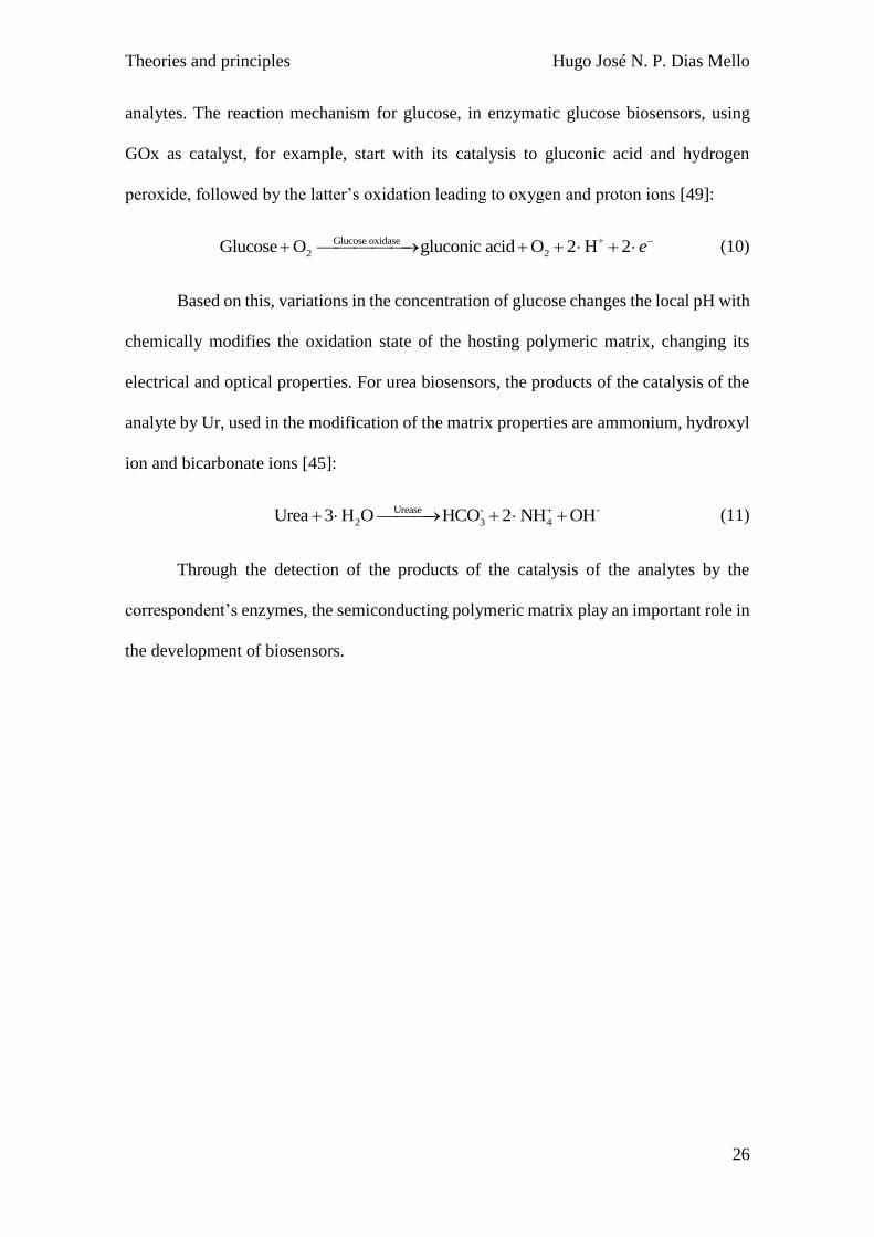
Theories and principles Hugo José N. P. Dias Mello
26
analytes. The reaction mechanism for glucose, in enzymatic glucose biosensors, using
GOx as catalyst, for example, start with its catalysis to gluconic acid and hydrogen
peroxide, followed by the latter’s oxidation leading to oxygen and proton ions [49]:
Glucose oxidase +
2 2Glucose O gluconic acid O 2 H 2 e−+ ⎯⎯⎯⎯⎯→ + + + (10)
Based on this, variations in the concentration of glucose changes the local pH with
chemically modifies the oxidation state of the hosting polymeric matrix, changing its
electrical and optical properties. For urea biosensors, the products of the catalysis of the
analyte by Ur, used in the modification of the matrix properties are ammonium, hydroxyl
ion and bicarbonate ions [45]:
Urease - -
2 3 4Urea 3 H O HCO 2 NH OH++ ⎯⎯⎯→ + + (11)
Through the detection of the products of the catalysis of the analytes by the
correspondent’s enzymes, the semiconducting polymeric matrix play an important role in
the development of biosensors.

Fabrication and application of PANI thin film Hugo José N. P. Dias Mello
27
3. Fabrication and application of PANI thin film
In this chapter, the structure-property relationship of PANI thin films fabricated through
the galvanostatic electrodeposition technique is presented. The influence of the
electrodeposition parameters on film’s properties, characteristics and response as pH
sensor was analysed [31,50]. The influence of deposition parameters such as current
density, deposition time, aniline monomer concentration, as well as the use of polymeric
blends, with polypyrrole were studied. Despite the potentiometric pH EGFET sensor, the
PANI thin films were applied on optochemical pH sensors due to their electrochromic
behaviour. The optochemical sensor measures the change in some optical parameter of
the chemically-sensitive film after its exposure to the target analyte [51–53].
Electrochemically deposited PANI thin films were already used as pH chemical
sensors. Chinnathambi and Euverink [54] reported the functionalization of
electrochemically reduced graphene oxide (ERGO) with PANI thin film by
electropolymerization of aniline as potentiometric and chemiresistive pH sensors for real
time monitoring pH change in a Lactococcus lactis bacterial fermentation. They
optimized the sensor adding a Nafion selective layer on top of the active sensing area of
the electrode to avoid interferences. They claimed that the developed pH sensor could be
used as a microsensor for real time pH changes monitoring in complex biological
processes.
PANI was also applied to the detection of heavy ions. Deshmukh and co-workers
have used electrodeposited PANI over indium tin oxide (ITO) electrodes for the detection
of Cu (II) ions through the chronoamperometric and electrochromic properties of the
polymer. The electrochromic effect was significantly altered after the incubation of the
samples in Cu (II) solutions and it was confirmed by the cyclic voltammetry analysis
which showed the electrochemical/electrochromic properties of the thin films [55].

Fabrication and application of PANI thin film Hugo José N. P. Dias Mello
28
Deshmuck and co-workers have also used PANI based composites with multi
walled carbon nanotubes (MWCNTs) for the detection of heavy metals based on the
electrochemical properties of the polymer. The detection was realized by an
electrochemical method, the differential pulse voltammetry (DPV) to analyse the
electrode after immersion in the proper solutions of the analytes. The PANI/SWCNTS
composite was modified with ethylenediaminetetraacetic acid (EDTA), which enhances
the selectivity of the electrode, for simultaneous and ultrasensitive detection of Cu, Pb
and Hg [56].
Several works can be found in the literature where the effects of processing and
fabrication conditions on the final properties of PANI have been studied. Zeng and Ko
showed that PANI synthesized by oxidative polymerization of aniline in a hydrochloric
acid aqueous solution using potassium dichromate as an oxidant presented increased
electrical conductivity. That was attributed to the iodine molar ratio dopant because the
iodine-doping reactions formed charge transfer complexes [57]. Wang et al showed that
PANI fibres in the emeraldine base oxidation state had their mechanical and electrical
properties varied when doped with varied amounts of secondary amine additives, because
the doping changed the gelation time [58].
Other works evaluated the relationship between parameters of samples
preparation of widely used chemical sensors materials, such as titanium dioxide (TiO2),
and EGFET sensors, showing that it is possible to establish a structure-property
relationship between films structure and EGFET response [59]. The characteristics and
structures of PANI films that influence their response as chemically-sensitive structures
in EGFET chemical sensor can also be studied, when they are produced by the
galvanostatic electrosynthesis, by changing and controlling the deposition parameters

Fabrication and application of PANI thin film Hugo José N. P. Dias Mello
29
related to the electrolyte solution polymerization, more specifically, the concentration of
aniline monomer in solution.
Another focus is the development of new materials based on conducting polymers
that present improved properties produced by the combination of more than one polymer
to obtain new materials such as copolymers, bilayers, composites or blends. The new
material usually presents improved physical, chemical, mechanical, and electrical
properties compared to the homopolymers [60].
Pašti and co-workers showed that resistive gas sensors based on carbonized
PANI/Nafion composites were produced and worked based on the sorption of gases
which induces Nafion swelling and consequently decreasing of conductivity of the
composite, which is dependent on the PANI conductive component. The system was able
to measure water, acetone, ethanol and methanol in a two- and four-point method [61].
Cellini, Grillo, and Porfiri, in turn, presented a technique to produce in-situ photoinduced
polymerization of polypyrrole-silver electrodes onto a ionomeric membrane, a class of
ionic polymer metal composite (IPMC) able to be used as sensing material being
dependent on the PPY properties and composition due to its ability to control the electrical
impedance and sheet resistance of the system [62]. Also, Di Pasquale and co-workers
demonstrated an ionic polymer-polymer composite (IP²Cs) system which is an all-organic
electroactive polymer (EAP) structure presenting sensing capability. They are based on
an ionic polymer, Nafion, coated on both sides with a conductive polymer, poly (3,4-
ethylendioxytiophene)-poly (styrene sulfonate) (PEDOT/PSS). The variation of the
polymerization time influences the uniformity of the surface of the organic electrode and,
consequently, both device stiffness and electrode conductivity, direct affecting the
sensing mechanism [63].

Fabrication and application of PANI thin film Hugo José N. P. Dias Mello
30
Regarding PANI and PPY, their copolymer can be prepared using the
galvanostatic technique in an organic acid medium [64,65]. A copolymer is made of
randomly distributed monomer subunits and possesses differing properties from that of
the homopolymers. Copolymers of PANI and PPY were also electrodeposited by
applying a varied potential [60,66], and applying a specific potential for a specific period
of time in an aqueous acid medium [67]. In the end, the properties of the copolymers
produced depended on the polymerization technique and on the electrolyte conditions.
The formation of bilayers is made by the deposition of one type of polymer over
a layer of another previously deposited polymer over a substrate [68]. For PANI and PPY,
it was possible to produce bilayers using an aqueous acid medium, using both a specific
potential for a specific period of time, applying an adequate polymerization potential
depending on the monomer [69], and using a varied potential [70]. A chemical synthesis
of PANI and PPY composite nanofibers were made by Liang et al., by injecting pyrrole
monomers into a PANI nanofiber dispersion used as seeds [71]. In all the previously
mentioned works, the relative monomer concentration was varied between aniline and
pyrrole to observe the influence of the monomer on the final polymeric composite.
PANI/PPY composite was electrochemically characterized presenting properties
that made it suitable to be used as supercapacitor due to its high specific capacitance and
good cycle stability when synthesized by electrosynthesis method with different aniline
and pyrrole ratios [72]. PANI/PPY composite was also electrodeposited for the corrosion
protection of copper bipolar plates in proton exchange membrane fuel cells (PEMFC). It
presented better protection than homopolymer coating which is ascribed to its tailored
structure [73]. This kind of film was also used as a temperature sensor, as described by
Karakişla and Saçak. They used a PANI/PPY bilayer structure deposited over a

Fabrication and application of PANI thin film Hugo José N. P. Dias Mello
31
polycarbonate-coated Pt electrode as temperature sensor by measuring its resistance
change with temperature [68].
The use of PANI/PPY blend thin films produced with variable relative monomer
concentration of aniline and pyrrole onto EGFET chemical sensors is presented. The
objective is based on the possibility to keep the polymer sensing mechanism properties
allied to a controlled sensitivity. The produced blend film’s structure-property
relationship showed a controllable sensitivity when the samples were applied as sensing
stage in EGFET devices as function of the relative monomer concentration.
As previously described, the electrochemical deposition technique is suitable to
produce PANI thin films due to the resultant film’s good homogeneity, strong adhesion
to the substrate, and chemical stability. Thin films of PANI were galvanostaticaly
electrodeposited and characterized by its morphology and spectral properties elsewhere
[74,75]. Two concepts related to galvanostatic electrodeposition are important. The
passivation charge is the charge that covers the substrate or electrode surface. It assumes
specific values that depend on the deposition conditions, such as, type of monomer,
polymerization solution, substrate/electrode material and current density [76]. The
passivation charge can be calculated using:
constantp pj t Q = = , (12)
where j is the current density, tp is the passivation time and Qp the passivation charge.
Those parameters can be obtained from the chronopotentiometric curves. Another
important concept, the deposition efficiency for polymers, can be de estimated by
comparing the measured film thickness with the theoretical film thickness, related to the
total deposited charge [77,78]. The calculated film thickness is given by the expression:
Wj t M
F z
=
, (13)

Fabrication and application of PANI thin film Hugo José N. P. Dias Mello
32
where j is the current density (mA/cm2), t is the deposition time (s), MW is the molecular
weight of the polymer (g/mol), F is the Faraday constant (C/mol), z is the number of
electrons transferred in the reaction and ρ is the polymer density (g/cm3). We intend to
study and to understand the influence of the galvanostatic electrodeposition parameters
of PANI thin films, more precisely the current density, deposition time, aniline monomer
concentration, and the use of polymeric blend of PANI/PPY, on EGFET and
optochemical reflectance pH sensors through the analysis of the relationship between the
material characteristics and device performance.
3.1. Methodology
3.1.1. Materials
Fluorine-doped tin oxide (FTO) thin films deposited on glass substrates were obtained
from Sigma-Aldrich and were used as substrate for PANI thin films. The FTO was chosen
due to its well-known properties, which include time stability, sensitivity and
performance as pH sensors [79]. The substrates were cleaned with de-ionized water
followed by acetone using the ultra-sonication method in order to remove contaminants
from the surface. Aniline (C6H5NH2) was supplied by Vetec Brazil and pyrrole (C4H5N)
and hydrochloric acid (HCl) by Sigma Aldrich.
3.1.2. PANI and PANI/PPY thin film synthesis
PANI thin films were synthesized via galvanostatic method. The polymerization was
carried out in a two-electrode system in a cell at 25 °C. The electric potential as a function
of time was recorded with a Data Acquisition model 34970A (HP). A platinum inert
electrode was used as counter electrode and FTO was used as working electrode. For the
evaluation of current density and deposition time influence on PANI thin film and its

Fabrication and application of PANI thin film Hugo José N. P. Dias Mello
33
effect on chemical pH sensor, the films were produced using polymerization solution
containing aniline monomer (0.1 mol/L), HCl (1.0 mol/L) and de-ionized water. The
current density was 0.5 and 1.0 mA/cm2. For each current density, three nominal
deposited charges were set: 150, 300 and 600 mC/cm2. To obtain these deposited charges,
the deposition time was varied. Table 3.1 presents sample identification, deposited
charge, current density and deposition time used.
Table 3.1 – Deposited charge of the PANI thin films. Current density and deposition time for each film are
shown. Sample identification is based on the current density and deposition time.
Deposited Charge
(mC/cm2)
1.0 mA/cm2 0.5 mA/cm2
Time (s) Identification Time (s) Identification
150 150 J10T150 300 J5T300
300 300 J10T300 600 J5T600
600 600 J10T600 1200 J5T1200
For the evaluation of the influence of aniline monomer concentration, the
polymerization solution contained aniline monomer in four distinct concentrations 0.10,
0.15, 0.20 and 0.25 mol/L (PANI films are thus identified by PANI10, PANI15, PANI20
and PANI25, respectively), HCl (1.0 mol/L. and de-ionized water. The current density
was 1.0 mA/cm2 and deposition time was 300 s, for a deposited charge 300 mC/cm2.
Finally, for the PANI/PPY blend, the polymerization solution contained aniline and
pyrrole monomer combined in a fixed final polymeric concentration of 0.25 mol/L, HCl
(1.0 mol/L. and de-ionized water in a 250 mL solution. The monomers were mixed in the
polymerization solution in five different proportions (90/10, 70/30, 50/50, 30/70 and
10/90). The final solutions were prepared adding the correspondent volume of monomer
to obtain the corresponding relative monomer concentration. Table 3.2 shows the

Fabrication and application of PANI thin film Hugo José N. P. Dias Mello
34
composition of each solution. Besides, the two independent homopolymer films, PANI
and PPY, were also produced. They correspond to samples 100/0 and 0/100, respectively.
The polymerization solution was deoxygenated by bubbling N2 for 15 min. [80]. The
solutions were put to rest for 18 h prior to run the deposition process.
Table 3.2 – Electropolymerization solution monomer concentration for each relative proportion. Aniline
and pyrrole monomer concentration for each solution for the constant final polymeric concentration of 0.25
mol/L. Sample identification is based on the relative monomer concentration.
100/00 90/10 70/30 50/50 30/70 10/90 00/100
Aniline (mol/L) 0.25 0.225 0.175 0.125 0.075 0.025 0
Pyrrole (mol/L) 0 0.025 0.075 0.125 0.175 0.225 0.25
Final conc. (mol/L) 0.25 0.25 0.25 0.25 0.25 0.25 0.25
3.1.3. Sample characterization
PANI thin films were characterized according to three criteria. The first one was
thickness. It was done using a precision profilometer (Taylor Hobson) with spatial
resolution of 0.1 nm. The second was morphology, which was studied using scanning
electron microscopy (SEM). A JEOL microscope JSM-6610 model operating at 20 kV
was used. A thin gold coating (~20 Å) was applied to the samples. The third characteristic
was the visible reflectance spectra. It was obtained non-destructively in the 400 nm to
700 nm range using a spectrophotometer model Colour-Guide, BYK-Gardner (Columbia,
USA). The data were recorded in 20 nm step with a 20 mm diameter circular aperture and
a 65/10° optical geometry. The device displayed the respective International Commission
on Illumination (CIE) colour values: luminance (L*), position between red and green (a*),
and position between yellow and blue (b*) [81]. For a polyelectrochromic and solid
material as PANI thin films, reflectance analysis is of great value.

Fabrication and application of PANI thin film Hugo José N. P. Dias Mello
35
3.1.4. Sensor measurement
In this section, the measurement procedure using the potentiometric EGFET and
optochemical sensors, as well as the structure of both sensors, is described. The same
devices were later used in biosensor measurements.
3.1.4.1. EGFET sensor
The EGFET sensor was based on the instrumental amplifier circuit using the CA3140
operational amplifier. This component was chosen due to its high impedance input stage
MOSFET. The instrumental amplifier circuit is a system with high input impedance and
stability, with changeable gain. The schematic of the sensor transducer structure is shown
in Figure 3.1.
Figure 3.1 – Experimental setup for the Instrumental Amplifier EGFET (IA-EGFET) system using the
CA3140 Op-Amp with unity gain
The complete experimental apparatus includes the sensor circuit device, a sensing
chamber which protects the sensing films connected to the sensor transducer, and the
reference electrode, both immersed in the analyte solution, and the data acquisition

Fabrication and application of PANI thin film Hugo José N. P. Dias Mello
36
34970A (HP) (to record the voltage generated by the transducer connecting it to a
personal computer for data analysis). The sensor transducer structure is formed by the
association of two CA3140 Op-Amps with the input stages connected to the sensing stage
and grounded (or associated to a reference/contrast film), with the outputs of these Op-
Amps connected to the input of the third CA3140 device, whose output is properly
recorded. The expression for the output voltage that is generated by the transducer is:
( )1 4OUT P C
2 3
2V 1 V V
R R
R R
= + −
, (14)
where VOUT is the output voltage, VP is the input voltage from the principal sensing stage
and VC is the input voltage from the contrast – reference – sensing stage. The sensor has
unity gain mainly due to output limitations of the integrated circuit. It was built with R1
= R4 = 1 kΩ and R2 = R3 = 2 kΩ [27,31,32].
For potentiometric sensor measurements, the sensing film is connected to the
principal input stage and then, dipped into the target solution. The electric potential is
recorded during 60 seconds for each solution (pH solutions, for example). An Ag/AgCl
reference electrode is dipped into the pH buffer solution to define its electric potential.
The films are carefully washed in de-ionized water in between each measurement. For
the next results to be presented, distinct PANI thin films were used as principal sensing
stage in EGFET pH chemical sensors. The positive charge equilibrium between PANI
sensing film and the solution determines the measured potentiometric values for each pH
solution.
3.1.4.2. Optochemical sensor
The optochemical sensor is composed of a target analyte, the transduction platform, and
eventually the electronics to process the information [51]. The reflectance optochemical

Fabrication and application of PANI thin film Hugo José N. P. Dias Mello
37
sensor uses a handset spectrophotometer which has a rapid and easy data analysis. The
visible reflectance spectra of the samples are measured nondestructively in the 400 nm to
700 nm range using a spectrophotometer model Color-Guide, BYK-Gardner (Columbia,
USA). A step of 20 nm is used with a 20 mm diameter circular aperture and a 65/10°
optical geometry. In these directional/directional diffuse reflectance measurements, the
sample is illuminated by an usually collimated light source [82]. The device displays the
respective International Commission on Illumination (CIE) color values: luminance (L*),
position between red and green (a*), and position between yellow and blue (b*), as
previously described in the previous section [53].
PANI thin films were used as the optochemical transducer. They were immersed
in each pH solution for 3 min before measurement of the reflectance spectra and colour
scale values. Both parameters were recorded as a function of the pH using the previously
mentioned spectrophotometer. The films were carefully washed in de-ionized water in
between each measurement.
3.1.4.3. Sensor parameters
The sensitivity (S) and linearity (L) are measured in the concentration range of each
analysis, and the pH buffer range is from 2 to 8. The sensitivity was obtained from the
sensor’s calibration curve. For the EGFET sensor its unity is mV/pH and for the optical
sensor it is integrated reflectance (IR) per pH, IR/pH, and the sensor’s linearity was
obtained from the coefficient of determination (R2) of fitted calibration curves. The
linearity parameter L is calculated by R2 times 100.
3.2. Influence of current density and deposition time
The chronopotentiometric curves and reflectance spectra of the PANI thin films are
shown in Figure 3.2. Figure 3.2 (a) shows that the induction time and the deposition

Fabrication and application of PANI thin film Hugo José N. P. Dias Mello
38
potential vary with the current density. This is expected because the passivation charge
should be kept constant with same polymerization solution and substrate for all samples.
Figure 3.2 – Chronopotentiometric curves for PANI deposition on FTO substrate at various current
densities in (a). Visible reflectance spectra of the PANI thin films in (b).
The passivation charge for the thin films was calculated using equation (10). The
mean value for FTO as substrate material is 150 ± 12 mC/cm2. The chronopotentiometric
curves for the films with larger current density have the highest potential values. This is
expected because the resistance of the system, given by the polymerization solution
resistance more the substrate resistance, was kept constant.
Figure 3.2 (b) shows the reflectance spectra of the PANI thin films. The
reflectance between 600 and 700 nm is larger for the set of films produced with current
density 1.0 mA/cm2 compared to the set of films produced with current density 0.5

Fabrication and application of PANI thin film Hugo José N. P. Dias Mello
39
mA/cm2, and the reflectance between 400 and 500 nm is larger for the set of films
produced with current density 0.5 mA/cm2 compared to the other one. Albuquerque et al
reported a similar behaviour for PANI thin films [83]. They analysed the absorbance
spectra. They showed that more oxidized PANI films have smaller absorbance between
600 and 700 nm which increases for less oxidized films. They also showed that more
oxidized PANI films have larger absorbance between 400 and 500 nm, which decreases
for less oxidized films. Du et al reported that PANI thin films produced with higher
current density are more oxidized having more quinoid rings than benzene rings, with low
potential for protonation [84]. Therefore, the films produced with 1.0 mA/cm2 are more
oxidized than the films produced with 0.5 mA/cm2 and present the corresponding
expected visible spectra.
The thickness, deposition efficiency and optical parameters of the PANI thin films
are shown in Figure 3.3. Figure 3.3 (a) shows the thickness of the PANI thin films
according to the deposited charge, for each current density. The film thickness increased
from deposited charge 150 mC/cm2 to 300 mC/cm2 and remains constant for deposited
charge higher than 300 mC/cm2. The film thickness is higher for current density 0.5
mA/cm2 than for 1.0 mA/cm2. As the film thickness reflects the efficiency of the
deposition process, there is a decrease in deposition efficiency with increasing current
density.
The peak in deposition efficiency occurs for deposited charge 300 mC/cm2, as
presented in Figure 3.3 (b). The deposition efficiency was calculated from the film
thickness, obtained using equation (13). The lowest current density has the highest
efficiency, with a peak at 300 mC/cm2 where the deposited charge has the highest
efficiency of 10 ± 1 %.

Fabrication and application of PANI thin film Hugo José N. P. Dias Mello
40
Figure 3.3 – Measured thickness of the PANI thin films in (a), deposition efficiency of the galvanostatic
polymerization in (b), and the optical parameters lightness (L*) and integrated reflectance in (c).
The galvanostatic deposition is a continuous process [85]. The application of
uninterrupted current for the formation of the thin films causes a competition between the
process of degradation and polymerization of the films [86]. For deposited charge 150
mC/cm2, a value that is equal to the passivation charge, the deposition process occurs
over the FTO substrate, what decreases the deposition efficiency. For deposited charge
300 mC/cm2, the deposition occurs first over the FTO substrate and then over a thin
polymeric sheet, increasing the deposition efficiency. For the deposited charge 600
mC/cm2, the deposition time increases, causing the degradation to be more important,

Fabrication and application of PANI thin film Hugo José N. P. Dias Mello
41
decreasing the deposition efficiency. The increase in current density provides a more
dynamic, less smooth and less controlled process, which cause a decrease in deposition
efficiency [87].
Figure 3.3 (c) shows the optical parameters lightness (L*) and integrated
reflectance, according to the deposited charge, for each current density. For the films
produced with current density 1.0 mA/cm2 the lightness and integrated reflectance reach
a peak. For the films produced with current density 0.5 mA/cm2 the lightness and
integrated reflectance decrease linearly with deposited charge. The optical response
depends on all the membrane structure [4]. There is equilibrium between deposition
efficiency and galvanostatic degradation in the polymerization process. For current
density 1.0 mA/cm2 the deposition efficiency is smaller making thinner films, that absorb
low light, and causing their reflexive optical responses to be higher. The film J10T150
has a lower optical response than expected, once that it is the thinner film, because as
deposition occurs predominantly over FTO substrate, the deposition efficiency is low,
producing PANI with worse structure characteristics, which decreases its optical
reflectance response. The deposition process of film J10T300 occurs over a thin
polymeric sheet at some period, what increases its deposition efficiency. The film is
thicker than J10T150, but its structure is more uniform making its reflective optical
response higher. Film J10T600 is the most degraded, having a completely irregular
structure, able to scatter more light that decreases the reflectance response. For 0.5
mA/cm2 the higher deposition efficiency guarantees a thicker film, and the lower
galvanostatic degradation for this current density does not influence the film structure
enough to change its optical response. Thicker films present lower reflectance optical
responses because they absorb more light.

Fabrication and application of PANI thin film Hugo José N. P. Dias Mello
42
The surface morphology of PANI thin films is shown in Figure 3.4. All the images
correspond to films with deposited charge of 300 mC/cm2. The micrographs were
enlarged 10,000 times. Figure 3.4 (a) shows the PANI thin film sample J5T600 while
Figure 3.4 (b) shows the PANI thin film sample J10T300 micrographs. This type of
structure is favoured by the galvanostatic electrodeposition technique.
Figure 3.4 – SEM images for PANI thin films galvanostatic deposited. All the samples have 300 mC cm-2
of deposited charge. The micrographs were enlarged 10000 times. In (a) the PANI thin film sample J5T300,
while in (b) the PANI thin film sample J10T300.
The film produced with current density 0.5 mA/cm2 has its polymeric matrix
better formed, presenting better coating of the substrate surface than the second film,
produced with current density 1.0 mA/cm2. Those qualities are directly related to the
current density magnitude. Smaller current densities can form more regular films with a

Fabrication and application of PANI thin film Hugo José N. P. Dias Mello
43
good polymeric surface coating. It also enables more polymer nucleuses to grow its own
branched structures. This occurs because the deposition efficiency is smaller for processes
with higher current density [87].
Figure 3.5 shows the potentiometric and optical sensor response, for the PANI
thin films for varied pH solutions. Figure 3.5 (a) shows the time response of the EGFET
sensor using sample J5T600, for increasing pH values. The other samples have similar
responses. The calibration curve is obtained by plotting the mean value, of three samples,
as function of the pH value. The inset shows the sensor structure. Figure 3.5 (b) shows
the response of the optical sensor using the same sample, J5T600. The spectra were
measured from 400 to 700 nm. Each presented curve is the reflectance spectrum for a
specific pH solution. The marked rectangle is the spectral green region, which integrated
values are used to construct the calibration curve.
The sensitivity and linearity of the EGFET and optical sensor for each set of PANI
thin films according to the deposited charge are presented in Figure 3.6. Figure 3.6 (a)
shows the variation of EGFET sensor sensitivity and Figure 3.6 (b) the variation in
EGFET linearity accordingly to the deposited charge. A maximum sensitivity of 81 ± 1
mV/pH and 70 ± 1 mV/pH was obtained, for current densities 0.5 and 1.0 mA/cm2,
respectively, for the films with deposited charge 300 mC/cm2. The film´s sensitivity
increases for deposited charge from 150 to 300 mC/cm2 because the amount of polymer
increased, and the surface characteristics of the films improved, as described before. The
sensitivity then decreases from 300 to 600 mC/cm2 because the deposition efficiency
decreases and the galvanostatic degradation for longer depositions degrades the thin film
surface. The EGFET sensor response depends mainly on the sensing material surface.

Fabrication and application of PANI thin film Hugo José N. P. Dias Mello
44
Figure 3.5 – Potentiometric and optical sensor response of the PANI thin films. (a) the IA-EGFET time
response for sample J5T600. The inset is the IA-EGFET sensor structure. (b) the response spectra of the
optical sensor using sample J5T600. The marked rectangle is the spectral green region.
The sensitivity is higher for films produced with current density equal to 0.5
mA/cm2, generally, because this is the current density value that has greater deposition
efficiency, producing films more effectively, with the polymeric matrix better formed and
non-degraded branched structures. Besides, they are less oxidized films with higher
protonation potential. The linearity was kept constant for films produced with current
density 0.5 mA/cm2 and presented a maximum for deposited charge 300 mC/cm2 for films
produced with 1.0 mA/cm2. The linearity is higher for density current 0.5 mA/cm2 than
for 1.0 mA/cm2 because the films from this last group has worst surface qualities and they
are more oxidized films with lower protonation potential.

Fabrication and application of PANI thin film Hugo José N. P. Dias Mello
45
Figure 3.6 – Sensor sensitivity and linearity are shown according to the total deposited charge. Response
for the IA-EGFET sensor in (a) and (b), and for the optical sensor in (c) and (d).
Figure 3.6 (c) shows the variation of optical sensor sensitivity and Figure 3.6 (d)
the variation in linearity according to the total deposited charge. Each current density has
a unique behaviour. Films produced using current density 1.0 mA/cm2 barely presented a
response being the high sensitivity 8 ± 5 IR/pH for sample J10T150. Films produced
using current density 0.5 mA/cm2 presented a linear response accordingly to the deposited
charge varying from 10 ± 1 IR/pH to 30 ±3 IR/pH. The worst quality of the films from
the first group saturates the optical response. The lower protonation potential, less
efficient deposition process and small polymeric volume of the PANI thin films,
influences directly the optical sensor that is directly dependent on all the structure
properties [53]. The second group of films has less oxidized PANI material with higher
protonation potential and it has higher deposition efficiency that guarantees a thicker film.

Fabrication and application of PANI thin film Hugo José N. P. Dias Mello
46
Thicker films can respond proportionally to pH because they do not saturate. The
response depends linearly with deposited charge.
The linearity better clarifies the differences in films sensing characteristics. The
linearity of films produced with current density 1.0 mA/cm2 increased with deposited
charge, reaching the higher value of 75.3 % for sample J10T600, because it produces a
thicker film, although it is not able to detect the ions in solution due to others poor
qualities of films. The linearity of the films produced with current density 0.5 mA/cm2
presented a slight decrease but it was not compromised (higher than 92 %) allowing the
sensors to be properly used.
All these presented results regarding PANI sensitivity when applied to
electrochemical (potentiometric) and optical pH sensor comes from the pH's influence on
the redox processes of the polymer. As previously discussed, upon protonic acid or
electrochemical doping/de-doping, the PANI materials can be protonated/deprotonated,
changing from PANI-EB to PANI-ES form, changing their properties. This is illustrated
in Figure 3.7.
The protonation by protonic acid occurs in the quinoid rings (imine nitrogen
groups) which presents a large affinity for charges, reaching an equilibrium between those
groups and the protons in the contact medium. This equilibrium generates a
potentiometric response possible to be measured. Also, as a polyelectrochromic material,
the changing between redox states generates variations in the polymer colour, also
possible to be measured and used.
The sensitivity and linearity of the optical sensor based on the CIE L*a*b* colour
system is shown in Figure 3.8. The data were obtained together with the visible spectrum
using the spectrophotometer Colour-Guide. The CIE L*a*b* colour system works as a

Fabrication and application of PANI thin film Hugo José N. P. Dias Mello
47
colorimetric scale to define colours in three axes. White–black (L*), red–green (a*) and
yellow–blue (b*) indicate the colour perceived by the human eye.
Figure 3.7 – Illustration of PANI protonation process. In contact with protonic acid, occurs the protonation
in the quinoid rings, which have high affinity for charges. This change can be detected by potentiometric
and optical measurements and used as sensor when measured as function of pH variation.
Figure 3.8 (a) and (b) shows the variation in sensitivity and linearity, respectively,
using the optical L*, a* and b* colour parameters accordingly to the total deposited charge
for the films deposited using current density 1.0 mA/cm2. Figure 3.8 (c) and (d) show the
same parameters for the films deposited using current density 0.5 mA/cm2. The graphs
are quite close to the graphs in Figure 3.6 for the optical sensitivity and linearity.
Regarding the L* parameter, the sensitivity increases linearly with deposited charge for
films produced with current density 0.5 mA/cm2, varying from 0.23 ± 0.02 1/pH to 0.94
± 0.15 1/pH, from sample J5T300 to J5T1200, respectively, and remains with practically
no response for films produced with current density 1.0 mA/cm2, the highest sensitivity
being 0.15 ± 0.11 1/pH for sample J10T150. The linearity slightly decreases for the first
group of films (higher than 85 %) and increases for the second group of films reaching
the highest value of 83 % for sample J10T600.

Fabrication and application of PANI thin film Hugo José N. P. Dias Mello
48
The parameter a* indicates the colour perceived by the human eye from red (+
a*) to green (– a*). The parameter b* indicates the colour perceived by the human eye
from yellow (+ b*) to blue (– b*). The sensitivity presents the same behaviour as before
(optical and L* sensor). Linear dependence to the deposited charge and useful values were
obtained for the set of samples deposited with current density 0.5 mA/cm2. Low and
useless sensitivities values were calculated for all the samples deposited with current
density 1.0 mA/cm2. This difference in the behaviour of the two set of films is almost
constant for all the optical sensors and it is related to the process of deposition and the
final sample characteristics and properties. The same is applied to the linearity.
Figure 3.8 – Colour scale optical sensor sensitivity and linearity accordingly to the total deposited charge
for three parameters: L, a* and b*. For the set of films deposited with current density 1.0 mA cm-2 in (a)
and (b) and current density 0.5 mA cm-2 in (c) and (d).
The useful sensitivity for both the colour parameter b* and the parameter a* (0.6
to 1.8 1/pH and 0.1 to 0.85 1/pH, respectively) for the set of films made with current

Fabrication and application of PANI thin film Hugo José N. P. Dias Mello
49
density 0.5 mA/cm2 is related to the main spectral variation of PANI upon protonation.
As discussed by Albuquerque et al [83] and Du et al [84], the protonation of PANI thin
film changes mainly the optical response between 400 and 500 nm and between 600 to
700 nm. These spectral bands are related to the blue/green band and to the yellow/red
band, respectively [88].
PANI thin films having a more oxidized structure, like PANI films produced with
current density 1.0 mA/cm2, are more electrically insulating and the protonated form can
be stabilized in highly acidic conditions (pH ~ 0). These features are explained by a strong
localization of the protonated ions in the polymer structure. This indicates that a high
electrical conductivity, as consequence of the structure protonation, can only be obtained
with films having a partial oxidized structure, like PANI films produced with current
density 0.5 mA/cm2 [89].
In summary, the control of galvanostatic electrodeposition parameters producing
PANI thin films led to variation in the response of the potentiometric EGFET chemical
sensor and the optochemical reflectance chemical sensor due to the differences in the final
PANI thin films structures. The sensitivity for the potentiometric sensor presented a peak
at deposited charge 300 mC/cm2 equal to 81 ± 1 and 70 ± 1 mV/pH for current density
0.5 and 1.0 mA/cm2, respectively. The optical sensitivity, both for reflectance spectrum
and CIE L*a*b* colour scale, increased linearly with deposited charge for current density
0.5 mA/cm2 that were always higher than for films made using current density 1.0
mA/cm2 that presented no response. The sensitivity of optochemical sensor reached a
maximum value for the deposited charge 600 mC/cm2 equal to 30 ± 3 1/pH. The
variations occurred because the potentiometric response depends mainly on the
chemically-sensitive material surface and the optical response depends on all the film
structure. Both thin film surface and bulk changed according to the deposited charge,

Fabrication and application of PANI thin film Hugo José N. P. Dias Mello
50
current density and deposition time because these parameters cause the polymerization
process to change, which led to thin films in distinct oxidation states. PANI films
produced with current density 0.5 mA/cm2 showed the best performance for both sensors
because they had a partial oxidized structure, emeraldine base, which have the higher
protonation potential and reaches a high electrical conductivity.
3.3. Influence of aniline monomer concentration
The chronopotentiometric curves and the reflectance spectra of the PANI thin films
deposited with different aniline concentrations are shown in Figure 3.9. Figure 3.9 (a)
shows the curves of the chronopotentiometric analysis, presenting an induction period
followed by a plateau that set the deposition potential, which is almost equal for all
samples. The induction period refers to the main period of the polymerization process,
when the polymer starts to be formed over the substrate. There is a relation between the
induction time and monomer concentration. The inset shows the variation of the induction
time of the galvanostatic deposited PANI films according to the aniline concentration.
The induction time was obtained from the chronopotentiometric derivative curves as the
time to the derivative to be null once the induction period is the time that the voltage takes
to increase and reach a near-constant value. The induction time was about 150 s for
sample PANI10 and decreased down to 70 s for sample PANI25. This behaviour is in
agreement with Conroy and Breslin [90]. Polymer formation time depends on the
monomer concentration, and this period is small for low monomers concentrations. This
occurs because the concentration of radical cations is low at this condition and,
consequently, generates a slow rate of electropolymerization.

Fabrication and application of PANI thin film Hugo José N. P. Dias Mello
51
Figure 3.9 – In (a), chronopotentiometric curves for galvanostatic deposited PANI thin films on FTO
substrate at various aniline concentrations. The inset shows the variation of the induction time of the PANI
films according to the aniline concentration. In (b), visible reflectance spectra of the galvanostatic deposited
PANI thin films. Sample PANI20 presents variations in the spectral response.
The reflectance spectra of the PANI thin films are shown in Figure 3.9 (b).
Specific bands are observed at 500, 600 and 675 nm. These characteristics of the
reflectance spectra are specific for PANI thin films [53], what allows us to conclude that
PANI thin films were produced indeed. Clearly, sample PANI20 has the highest spectral
intensity between 400 and 525 nm and the lowest spectral response between 550 and 700
nm, when compared to the other samples which are alike. The behaviour of this sample
is believed to be related to the optimization of the polymerization process for this
concentration of aniline monomer. It is already known that the PANI film with the best
physical, chemical and structural properties presents a similar behaviour, with high

Fabrication and application of PANI thin film Hugo José N. P. Dias Mello
52
intensity from 400 to 520 nm and low intensity from 550 to 700 nm [83]. This optimized
process occurs for the best combination of the deposition efficiency and deposition rate,
once that both influence the film structure.
The thickness, optical parameters and an illustration of the theoretical model of
PANI thin films galvanostatic electrodeposited are shown in Figure 3.10. Figure 3.10 (a)
shows the thickness of PANI thin films according to the aniline concentration. The
thickness of PANI thin films first increases from sample PANI10 to sample PANI20
(from 54 ± 3 nm to 121 ± 5 nm, respectively), where it reaches a maximum and then
decreases down to 68 ± 3 nm for sample PANI25. This behaviour is related to a
competition between the deposition efficiency and deposition rate for the polymer, where
each one varies with aniline monomer concentration. The deposition efficiency describes
the quality of the polymerization process and the deposition rate describes how much
polymer is deposited per unity time.
Figure 3.10 (b) shows the optical parameters lightness (L*) and integrated
reflectance, according to the aniline monomer concentration. Both parameters varied in a
similar way: they decreased from sample PANI10 to PANI20 and then they increased for
sample PANI25. This behaviour is reversed in relation to the previously discussed
thickness. This happens because thicker films absorb more light, decreasing their
brightness and spectral reflectance intensity. In this way, the optical parameters are also
dependent on the deposition process that has a competition between deposition efficiency
and deposition rate.
Mondal et al showed by the analysis of polymeric films bulk resistance variation,
deposited by electrochemical methods, that the deposition efficiency remains
approximately constant until a threshold value at which the increasing concentration of
aniline causes a decrease in deposition efficiency [86]. Sazou and Georgolios showed,

Fabrication and application of PANI thin film Hugo José N. P. Dias Mello
53
studying PANI films deposited by electrochemical methods, that the decreasing
efficiency of PANI deposition is caused by a low concentration of the acid in the
polymerization solution compared to the aniline monomer concentration [91].
Figure 3.10 – Measured thickness of PANI thin films in (a), the optical parameters lightness (L*) and
integrated reflectance in (b) and the theoretical model for the deposition efficiency and deposition rate for
the galvanostatic deposited PANI thin films in (c) as a function of aniline concentration.
Figure 3.10 (c) shows an illustration of the theoretical model considering the
competition between deposition efficiency and deposition rate. The determination of this
critical point, that defines the more efficient regime, depends on several parameters of the
polymerization process and polymerization solution, like type and concentration of the
acid, monomer concentration, deposition technique, current density and deposition time.

Fabrication and application of PANI thin film Hugo José N. P. Dias Mello
54
For galvanostatic polymerization of PANI in an acid aqueous solution with aniline, the
deposition efficiency changed for a monomer concentration around 0.20 mol/L. The
efficiency drop of the polymerization process is demonstrated by the decreased thickness
of sample PANI25, while for the other samples, with low aniline concentration, the
deposition efficiency is approximately constant although the thickness is also decreasing.
This happened due to the variation in the deposition rate of PANI. In the low
concentration monomer regime the deposition rate increased proportionally to the
monomer concentration until reaching an approximately constant value [74,92,93]. The
increasing deposition rate is demonstrated by the increased thickness from sample
PANI10 to PANI20. The two effects combined, deposition rate and deposition efficiency,
give the observed thickness and optical pattern.
The variation of aniline monomer concentration also influences the response of
thin films when used in EGFET potentiometric sensors. The sensitivity and linearity of
the EGFET sensor made with PANI thin films are shown in Figure 3.11, with data being
plotted according to aniline concentration. The sensor’s sensitivity remains practically
constant from sample PANI10 to PANI20, 70 ± 1 and 68 ± 1 mV/pH, respectively,
presenting a maximum decrease of about 4.4 %. Then, the sensitivity drops between
sample PANI20 to PANI25 that has sensitivity 57 ± 1 mV/pH, 19 % when compared to
the first one. The sensitivity values were obtained for the pH buffer range from 2 to 8
indicating that the variation in the pH of the medium influences the
protonation/deprotonation process in PANI films, making it able to work as pH sensors.
All samples presented high linearity, above 99.6%. It is important to note that the
comprehension of the relationship between the structure of PANI thin films prepared with
different aniline concentrations and the sensitivity of pH EGFET chemical sensors is the
primary focus regarding the goal for tuneable sensitivity of chemically-sensitive

Fabrication and application of PANI thin film Hugo José N. P. Dias Mello
55
structures, especially for future applications. Further studies should focus on selectivity,
hysteresis, durability and other important features of chemical sensors. However, based
on previous studies regarding the basic physical-chemistry of pH chemical sensors based
on PANI thin films it is expected that the response of electrochemically synthesized PANI
films to be compatible with the proposed applications [31].
Figure 3.11 – IA-EGFET sensor sensitivity (left y-axis) and linearity (right y-axis) are shown accordingly
to the aniline monomer concentration. In the far-right y-axis it is shown the electrodeposition efficiency
curve, which is clearly over the sensitivity variation.
The EGFET sensor response is related to the deposition efficiency because the
efficiency of polymerization can change the morphology and structure of the surface of
PANI thin films and the potentiometric sensors depend mainly on the chemically-
sensitive films surface, due to its interaction with the target analyte in solution. The
decrease in the sensitivity of the chemical sensor is related to the drop-in deposition
efficiency, which is estimated using the thickness of the samples. In this way, from the
thickness measurement it is possible to estimate the deposition efficiency of each sample
produced and correlate it to the EGFET sensitivity once that the deposition efficiency
determines the surface characteristics of the thin films.
The morphology of the surface of PANI thin films are shown in Figure 3.12.
Results for samples PANI10, PANI15, PANI20 and PANI25 are shown in Figure 3.12
(a), (b), (c) and (d), respectively. From PANI10 to PANI20 there is an increment of the

Fabrication and application of PANI thin film Hugo José N. P. Dias Mello
56
surface coverage by the polymeric material, due to the increasing deposition rate. The
morphology of the starting substrate, that is clear in the picture for sample PANI10,
becomes less apparent for increasing monomer concentrations because the polymeric
matrix is better formed for those films. That can be noted by the analysis of the differences
in grey scale variation of the images. The black-to-white window difference decreases
until sample PANI20 and that can be correlated to a decrease in the morphologic variation
in the samples caused by the increment of surface coverage, as already described, which
makes the images more homogeneous. The PANI structures that are formed somehow
follow the substrate morphology in the beginning. As the aniline monomer concentration
increases, this dominance is less perceived once the polymerization nuclei are more
numerous. The samples presented a granular form, and each grain acts as a nucleus for
PANI polymerization.
For sample PANI25 there is a decrease in surface coverage, and the sample also
presents a modification in the morphology when compared to the other samples. PANI25
has a different granular characteristic, presenting grains with a spherical-like shape.
Again, it is possible to note that the differences in grey scale return to the level of the first
sample. This modification of surface morphology is caused by the variation in the
electrodeposition efficiency. The decreasing electrodeposition efficiency worsens the
surface quality of the formed thin film. Because of this behaviour, the usefulness of the
films as chemically-sensitive stage in potentiometric chemical sensors might be
compromised. This was indeed observed in EGFET sensors, Figure 3.11. Sample PANI20
(Figure 3.12 (c)) seems to have the most regular surface, being smoother and with a larger
amount of deposited polymer, which is related to the fact that this thin film was made
with the optimized relation between deposition rate and deposition efficiency, also
presenting the largest thickness.

Fabrication and application of PANI thin film Hugo José N. P. Dias Mello
57
Figure 3.12 – SEM images for PANI thin films galvanostatic deposited varying the aniline monomer
concentration. Samples PANI10, PANI15, PANI20 and PANI25 are shown in (a), (b), (c) and (d),
respectively.
In summary, the characteristics and structure of PANI thin films galvanostatic
electrodeposited varied with the aniline monomer concentration in the polymerization
solutions, establishing a structure-property relationship concerning the EGFET chemical
sensor. Varying the concentration of aniline in from 0.10M to 0.25 mol/L the induction
time decreased proportionally to the monomer concentration. The thickness of PANI thin
films presented a maximum value of 121 ± 5 nm for a sample deposited with 0.20M. The
optical properties presented a reverse behaviour compared to the thickness, as expected,
with small intensity of brightness and optical reflectance for this same sample, once that
the thicker sample absorbs more light. The morphology of the samples also varied with
monomer concentration, and up to 0.20M the films presented a regular and homogeneous

Fabrication and application of PANI thin film Hugo José N. P. Dias Mello
58
surface coverage, what changed for sample larger monomer concentration. The EGFET
sensitivity had little variation for samples prepared with monomer concentrations up to
0.20M. Good sensitivities close to 70mV/pH were found, but this parameter presented an
important drop for larger concentrations. The thickness, optical and morphology
characteristics presented for the PANI films are explained by the competition between
deposition rate and deposition efficiency during PANI polymerization with varied aniline
concentration. Samples fabricated with monomer concentrations of 0.20M represent the
optimized case.
3.4. PANI/PPY composite thin films
The chronopotentiometric curves for the electrodeposition process are shown in Figure
3.13 (a). The curves correspond to PANI, PPY and PANI/PPY composite in the
proportion 50/50. The induction time increases and the deposition potential decreases
from sample PANI to PPY. PANI film has a faster deposition than PPY film, as can be
seen by the difference in induction time, which is approximately 25 and 200 s, for PANI
and PPY, respectively. Film 50/50 has a specific intermediate behaviour. When the
monomers proportion is equal, there is a competition between both electrodeposition
processes, of aniline and pyrrole, reflected by the chronopotentiometric curve, specially,
between 25 and 75 s, where it is not possible to define an appropriate behaviour for the
deposition process. The curves of the other films, depending on the relative monomer
proportion, present a proportional behaviour in between the two extreme cases.
The electrochromic property of some conducting polymers, such as PANI and
PPY, comes from a protonation/deprotonation reaction that leads to colour change from
blue to green, reversibly, and an interesting way to evaluate this property is by reflectance
spectroscopy [94]. The normalized reflectance spectra of the PANI/PPY thin films are
shown in Figure 3.13 (b). There are variations in the reflectance peaks of all samples,

Fabrication and application of PANI thin film Hugo José N. P. Dias Mello
59
from the homopolymer PANI film to the homopolymer PPY film, indicating that the
material of the thin films is different. The main spectral peaks and valleys are indicated
by arrows in the figure. The higher peaks and valleys come from PANI homopolymer and
the intensity for the PANI/PPY composites decreased proportionally down to the PPY
homopolymer values, indicating that the relative concentration between PANI and PPY
is determinant for the composite’s optical response.
Figure 3.13 – Chronopotentiometric curves of the PANI, 50/50 PANI/PPY and PPY samples in (a). These
curves are representative of the others composite samples, which lie in between these, depending on the
relative monomer proportion. Normalized reflectance spectra for all thin films of the copolymer PANI/PPY
in (b). The relative intensity varies from the PANI to the PPY sample accordingly to the relative monomer
concentration.
The optical parameters of PANI/PPY thin films are shown in Figure 3.14. The
integrated reflectance and the brightness (L*) are shown in Figure 3.14 (a) and the CIE

Fabrication and application of PANI thin film Hugo José N. P. Dias Mello
60
L*a*b* colour scale parameter a*, which varies from red to green, is shown in Figure
3.14 (b). Both the integrated reflectance and L* reach their largest values for PANI
homopolymer thin film and the smallest ones to PPY, as can be seen in Figure 3.14 (a).
Besides, the parameters linearly decrease from sample PANI down to sample 50/50. After
that, for increasing PPY proportions there are practically no variation in these optical
parameters. The optical parameters only changed for the composite films in which PANI
proportion is higher than PPY, thus indicating again that the concentration of PANI is
determinant for the composite`s optical response. The behaviour of colour parameter a*
is shown in Figure 3.14 (b). There is a monotonic decrease in its value from PANI
homopolymer (100/00) to PPY homopolymer (00/100), being directly proportional to the
relative monomer concentration. As previously discussed, the concentration of PANI is
determinant for the composite’s optical response, thus making the analysis of the colour
variation, from green to red, as an indicator for the proportion of the polymers in the
composite. This colorimetric technique proved to be accurate [53]. It was used to develop
an optochemical sensor through the evaluation of electrodeposited PANI thin films as
function of the pH of the measured solution. The PANI samples changed its oxidation
states due to protonation/deprotonation and the system was able to distinguish up to 7
different PANI states.
The optical reflectance characteristic of PANI/PPY composites can be correlated
to the thickness of the samples. The optical response is proportional to the total amount
of polymer deposited. Thicker films absorb more light and have lower reflective
responses [4]. The PANI film, which is the thinnest sample, has the largest relative
reflectance peak intensity. This intensity varies down to the PPY sample. To obtain a fully
description of the samples, films with comparable thickness and different composition

Fabrication and application of PANI thin film Hugo José N. P. Dias Mello
61
could be further evaluated. In this study, the aim was to verify the effect of the composite
composition on the structure-property relationships and how it could be controllable.
Figure 3.14 – Optical parameters integrated reflectance and brightness (L*) of the PANI/PPY composite
thin films in (a). The response is related to the thickness of the samples and its composition. Colour
parameter a* of the PANI/PPY composite film in (b). Its variation is sensitive to the composition. The
thickness of the samples is shown in (c). The deposition efficiency is improved in cases where pyrrole
predominates
The thickness of the PANI/PPY composite thin films are shown in Figure 3.14
(c). The values varied from 68 ± 10 nm for the PANI homopolymer thin film to 561 ± 33
nm for the PPY homopolymer thin film. The thickness of the thin films does not present
a significant change till sample 50/50. After this proportion, it linearly increases till the
PPY homopolymer thin film final value. The galvanostatic electropolymerization of

Fabrication and application of PANI thin film Hugo José N. P. Dias Mello
62
pyrrole is more efficient than aniline when they are synthesized together. Abaci et al
showed that the deposition efficiency of PPY over PANI was improved and that PANI
over PPY was worsened, when compared to the homopolymers over ITO substrates [78].
Basically, the deposition of pyrrole is favourable in an aniline environment while the
opposite is not true.
The thin films that are thinner (from PANI homopolymer to 50/50) have higher
optical response and the thicker films have lower optical response, as expected. However,
for samples in the range where there is no variation in the thickness of the films, their
optical parameters varied proportionally. That is related to the thin film composition.
Films that are made mostly of aniline have better reflexive optical response than films
made mostly of pyrrole. Not only the thin film thickness but also the composition of them
influences the optical response depending on the electrodeposition process. Thinner
samples presented higher reflectance response, but variations were only able to be
detected for samples with variation on the composition, specifically, the aniline amount.
Differently to the other optical parameters that are dependent on a combination of
properties, such as relative composition of the monomers and film thickness, the colour
parameters from CIE L*a*b* scale are subtler and sensitive to detect variation in the thin
film’s composition. Specific the colour parameter a*, that measures the variation from
green to red, can estimate both the variation in aniline and/or pyrrole concentration.
The surface morphology of PANI/PPY composite thin films are shown in Figure
3.15. Figure 3.15 (a) is the micrograph of the FTO substrate, Figure 3.15 (b) corresponds
to the PANI homopolymer film, Figure 3.15 (c) corresponds to PANI/PPY 50/50
composite film and Figure 3.15 (d) corresponds to the PPY homopolymer film. The
surface of PANI thin film has a granular structure while the PPY thin film has a spherical
structure, as shown elsewhere [67]. Comparing them to the FTO sample, it is possible to
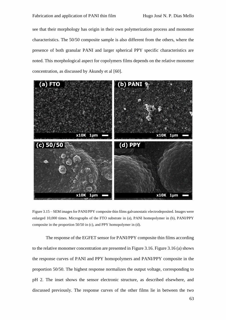
Fabrication and application of PANI thin film Hugo José N. P. Dias Mello
63
see that their morphology has origin in their own polymerization process and monomer
characteristics. The 50/50 composite sample is also different from the others, where the
presence of both granular PANI and larger spherical PPY specific characteristics are
noted. This morphological aspect for copolymers films depends on the relative monomer
concentration, as discussed by Akundy et al [60].
Figure 3.15 – SEM images for PANI/PPY composite thin films galvanostatic electrodeposited. Images were
enlarged 10,000 times. Micrographs of the FTO substrate in (a), PANI homopolymer in (b), PANI/PPY
composite in the proportion 50/50 in (c), and PPY homopolymer in (d).
The response of the EGFET sensor for PANI/PPY composite thin films according
to the relative monomer concentration are presented in Figure 3.16. Figure 3.16 (a) shows
the response curves of PANI and PPY homopolymers and PANI/PPY composite in the
proportion 50/50. The highest response normalizes the output voltage, corresponding to
pH 2. The inset shows the sensor electronic structure, as described elsewhere, and
discussed previously. The response curves of the other films lie in between the two

Fabrication and application of PANI thin film Hugo José N. P. Dias Mello
64
extreme cases, depending on the relative monomer proportion. The summary of the
analysis is shown in Figure 3.16 (b), using the sensitivity and linearity of the samples.
The sensitivity exponentially decayed from its highest value 57 ± 1 mV/pH for PANI
homopolymer sample, down to its lowest value 25 ± 1 mV/pH for PPY homopolymer
sample. The sensitivity for sample 50/50 was 32 ± 1 mV/pH. The linearity of all samples
is also shown at the right axis of Figure 3.16 (b). It is never lower than 98 %.
Figure 3.16 – Response of PANI/PPY composite thin films as IA-EGFET chemical sensors. The calibration
curves of the PANI and PPY homopolymers and for the PANI/PPY composite in the proportion 50/50 are
shown in (a) together with the IA-EGFET sensor structure in the inset. The behavior of the sensitivity and
linearity for the films is shown in (b).
PANI thin film applied for pH sensor has presented higher sensitivity, in the range
of 75-80 mV/pH [31], however, most of the pH sensors based on PANI films presented
similar sensitivity, in the range of 55-65 mV/pH [4,54,95,96]. For galvanostatic
electrodeposited PANI thin films applied as pH sensor, we have shown that the aniline
monomer concentration is fundamental in the final sensitivity, and for higher monomer

Fabrication and application of PANI thin film Hugo José N. P. Dias Mello
65
concentration, as 0.25 mol/L, there is a decrease in the sensitivity [97]. Also for PPY thin
films applied as pH sensor, the sensitivity lies in the range of 32-53 mV/pH depending
on the deposition process [98]. The obtained value of 25 mV/pH is justified by the
polymerization conditions. The results presented show that it is possible to obtain
controllable sensitivities for FET based pH sensor using PANI/PPY composite thin films.
PANI thin films are known as good chemically-sensitive materials for chemical
sensors [4,31]. PPY thin films are also very used in chemical sensors, presenting good
sensitivity and linearity values [98,99]. Two factors explain the low sensitivity of PPY
homopolymer film as EGFET sensor in this study: thicker films of PPY have lower
sensitivity as solid state chemical sensors [98] and the aqueous acid electrolyte used as
polymerization solution medium is not the favourable one for PPY. PPY thin films
presented better characteristics and properties when they are polymerized in organic acid
medium [100]. This is also the case for PANI/PPY composites with prevalence of pyrrole
in the polymerization solution [65,67]. The electrolyte used in the galvanostatic
electrodeposition of PANI/PPY composite thin films was composed of a strong inorganic
acid, which is not favourable to PPY deposition but it is to the deposition of PANI
[64,101], which made the deposited composite thin films with prevalence of aniline in
the polymerization solution to present superior properties. The characteristics of the
electrolyte used in the deposition of the thin films is relevant to their final response as
chemical sensor once that it plays an important role in the properties of the deposited
material [69]. Karakişla and Saçak stated that the properties of the composite thin films
vary between the properties of their respectively homopolymers and are directly
dependent to the relative monomer concentration [68]. This was also discussed by
Kanazawa et al. and Inganäs et al [102]. As the polymerization solution is based on an

Fabrication and application of PANI thin film Hugo José N. P. Dias Mello
66
environment favourable to the PANI electrodeposition, the deposited composite thin
films have a prevalence of features of PANI front of PPY.
The comparison between the chemical sensor sensitivity of the PANI/PPY
copolymer thin films and the optical integrated reflectance parameter is shown in Figure
3.17. This graph shows that these properties of the PANI/PPY composite thin films are
correlated to each other. The region where the thin films composition is dominated by
pyrrole presented low optical variation, and the region dominated by aniline monomer
presented a proportional variation between the main potentiometric property, the
chemical sensitivity, and the most comprehensive optical property, integrated reflectance,
which is responsible to inform about the whole film property and composition. These
results corroborate the previous discussion where it was stated that the properties of the
composite films vary between the properties of the two homopolymers, PANI and PPY
in our case, being PANI the favourable material due to the electrodeposition conditions,
presenting tuneable pH sensitivity and optical integrated reflectance parameter from the
PANI homopolymer to the 50/50 composite.
Figure 3.17 – Comparison between the chemical sensor sensitivity of the PANI/PPY composite thin films
and the optical integrated reflectance parameter.

Fabrication and application of PANI thin film Hugo José N. P. Dias Mello
67
In summary, the electrodeposition of PANI/PPY composite was possible despite
the different requirements of the polymerization conditions for each individual
homopolymer. Thin films of PANI and PPY homopolymers and PANI/PPY composites
with varied relative monomer concentration were synthesized via a galvanostatic
electrochemical method in an aqueous acid medium. The properties of the composite thin
films varied between the properties of the corresponding homopolymers and were
dependent of the relative monomer concentration. In an aqueous acid medium, PANI
polymerization is favourable, and the properties of the composite thin films varied from
the values of PANI homopolymer down to PPY homopolymer. The thickness of the thin
films varied from the PANI (68 ± 10 nm), to the PPY homopolymer (561 ± 33 nm),
presenting significant change for films produced with higher concentration of pyrrole.
Once the optical response of polymeric thin films is based on the thickness and
composition, the reflexive spectra and optical parameters varied from the higher response
for PANI thin film down to PPY. To the EGFET chemical sensor, the sensitivity varied
from 57 ± 1 mV/pH for the PANI sample, down to 25 ± 1 mV/pH for the PPY sample,
accompanying the optical response, determined by the electrodeposition conditions. The
sensitivity variation was exponential, and it was possible to change the sensitivity of the
sensor accordingly to the relative monomer concentration.

Biosensors based on PANI thin film Hugo José N. P. Dias Mello
68
4. Biosensors based on PANI thin film
In this chapter, the use of functionalized PANI thin films with glucose oxidase and urease
enzymes through the one-step electrochemical immobilization process into
potentiometric enzymatic field-effect-transistor (EnFET) biosensors is described. The
structure-property relationship of the immobilization matrix is discussed concerning the
properties presented by the biosensor such as sensitivity, linearity, detection range, long
term stability, repeatability and selectivity. The analysis of the use of such thin films in
conductometric (by electrochemical impedance spectroscopy, EIS) and optical biosensors
are also described. Stablishing the FET based enzymatic biosensor with functionalized
PANI thin film, a multimodal array of enzymatic biosensors is described, presenting its
advantages and technological improvements.
Conducting polymers are of interest for biosensors because they can function as
the biological recognition stage immobilization matrix, hosting enzymes, cells, DNA
strands, among others. These conducting polymers are used to increase the speed,
sensitivity and versatility of biosensors [103]. Their use allows the immobilization of
molecules of varying sizes and geometry and is particularly suitable for the manufacture
of miniaturized biosensors for the analysis of various analytes. Conducting polymers have
considerable flexibility in their chemical structure, which can be changed as required.
Through chemical modelling or the synthesis process, it is possible to modulate the
electronic and mechanical properties of these polymers, thus presenting advantages for
the connection to the biological elements of interest. Another important advantage of the
use of conducting polymers is the fact that their electrochemical synthesis, i.e.,
electrodeposition, allows the direct deposition of the polymer on the surface of the
electrode with simultaneous entrapment of enzymes, the one-step immobilization
electrodeposition technique [104–108]. Therefore, it is possible to control the spatial

Biosensors based on PANI thin film Hugo José N. P. Dias Mello
69
distribution of the enzymes, film thickness, modulating the enzymatic activity by altering
the state of the polymer. As for its use in conjunction with different transduction systems,
in the specific case of potentiometric biosensors, the sensitivity of the conducting
polymers to the pH variation or the presence of specific ions, results in a change in the
energy levels, band levels, or work function of the polymer, which is consequently felt
by the potentiometric system.
PANI has been extensively used in the development of enzymatic biosensors,
mainly due to its relative low cost and easy synthesis from aniline monomer in aqueous
solution, easy doping/de-doping process, which can remarkably change its electronic
structure, magnetic properties, electrical conductivity and others, high surface area and
chemical specificities, redox conductivity and polyelectrolyte characteristics, direct and
easy deposition on electrodes, biocompatibility, excellent environmental stability and
effective anti-interferences property, the ability to control PANI properties by varying
electrochemical polarization conditions and its ability to be not only the immobilization
matrix but also the electron mediator in a redox or enzymatic reaction due to its excellent
conductivity and inherent electroactivity [48,109]. Such functionalized thin films are used
on potentiometric EnFET, conductometric and optical biosensors.
Among the many transduction procedures enumerated already for the biosensors,
one can cite the electrochemical cyclic voltammetry (CV), amperometric, potentiometric,
such as field-effect transistor (FET) based devices, calorimetric and piezoelectric devices.
Two other transducer systems, the conductometric and optical biosensors, are also
applied. Regarding the first one, conductometric, the EIS is one of the most powerful and
versatile techniques used for investigating electrochemical systems and processes. It is a
non-destructive steady-state method capable to analyse the complex electrochemical
system over a wide range of frequencies providing information about the sensing layer’s

Biosensors based on PANI thin film Hugo José N. P. Dias Mello
70
impedance. The EIS method has been widely used for investigation of electrochemical
reactions in sensors, semiconductor devices, batteries [110]. For the second one, an
optical biosensor is based on the measurement of light absorbed, emitted or reflected of
the system as consequence of a biochemical reaction [111]. The use of functionalized
PANI thin films is interesting as reflectance optical biosensors because it is a solid-state
sample based on polymers, allowing the detection of reflected light in specific visible
bands of the spectra.
Combining the PANI property which is the capability of changing its electrical
and optical properties depending on the chemical environment we use it as support
material for glucose and urea biosensor based on electrochemical impedance
spectroscopy and optical reflectance transducer methods, evaluating not only its
sensitivity and linearity but also the evolution over time.
The combination of different sensors on a common base allow one to analyse
distinct analytes simultaneous. This also permits to increase the reliability of the system
and decreases the time needed to make distinct measurements. An array of sensors, in this
way, offer better functionality than is common with traditional arrangements. This could
help to overcome the limited use of biosensors, that occurs due to the lack of ability to
sensing a specific analyte among various compounds in a same real sample [112]. The
multimodal array of enzymatic biosensors (MAEB) is a device built using the
functionalized PANI thin films as sensing stages connected to an EGFET transduction
stage, in a system adapted to environmental changes. The differential mode of operation
is defined by using a reference sensing stage to decrease the influence of environmental
parameters [32]. A multiplexer device is used to select the appropriate input to be ready
by the transduction system which is controlled by a microcontroller device.
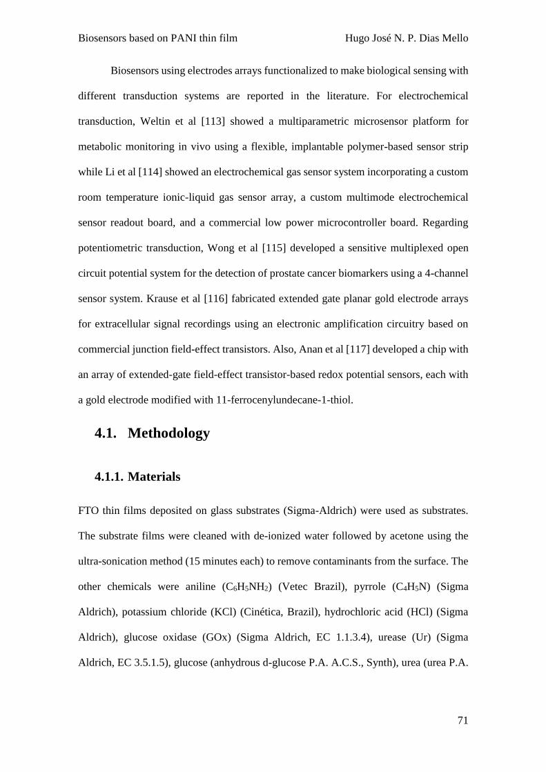
Biosensors based on PANI thin film Hugo José N. P. Dias Mello
71
Biosensors using electrodes arrays functionalized to make biological sensing with
different transduction systems are reported in the literature. For electrochemical
transduction, Weltin et al [113] showed a multiparametric microsensor platform for
metabolic monitoring in vivo using a flexible, implantable polymer-based sensor strip
while Li et al [114] showed an electrochemical gas sensor system incorporating a custom
room temperature ionic-liquid gas sensor array, a custom multimode electrochemical
sensor readout board, and a commercial low power microcontroller board. Regarding
potentiometric transduction, Wong et al [115] developed a sensitive multiplexed open
circuit potential system for the detection of prostate cancer biomarkers using a 4-channel
sensor system. Krause et al [116] fabricated extended gate planar gold electrode arrays
for extracellular signal recordings using an electronic amplification circuitry based on
commercial junction field-effect transistors. Also, Anan et al [117] developed a chip with
an array of extended-gate field-effect transistor-based redox potential sensors, each with
a gold electrode modified with 11-ferrocenylundecane-1-thiol.
4.1. Methodology
4.1.1. Materials
FTO thin films deposited on glass substrates (Sigma-Aldrich) were used as substrates.
The substrate films were cleaned with de-ionized water followed by acetone using the
ultra-sonication method (15 minutes each) to remove contaminants from the surface. The
other chemicals were aniline (C6H5NH2) (Vetec Brazil), pyrrole (C4H5N) (Sigma
Aldrich), potassium chloride (KCl) (Cinética, Brazil), hydrochloric acid (HCl) (Sigma
Aldrich), glucose oxidase (GOx) (Sigma Aldrich, EC 1.1.3.4), urease (Ur) (Sigma
Aldrich, EC 3.5.1.5), glucose (anhydrous d-glucose P.A. A.C.S., Synth), urea (urea P.A.

Biosensors based on PANI thin film Hugo José N. P. Dias Mello
72
A.C.S., Vetec Brazil), anhydrous bibasic sodium phosphate (P.A.-A.C.S. Synth), sodium
phosphate monobasic (P.A.-A.C.S. Synth).
4.1.1.1. Functionalized PANI thin films
The functionalized PANI thin films were obtained by the galvanostatic entrapment of
enzymes. The electropolymerization of PANI and enzyme entrapment were conducted
galvanostaticaly in a one-step process, by applying a desirable current density for a
specific deposition time. A platinum inert electrode was used as counter electrode and
FTO was used as working electrode. The aqueous polymerization solution contained
aniline monomer (0.1 mol/L), KCl (0.1 mol/L), de-ionized water and glucose oxidase or
urease, respectively for each kind of biosensor, in specific concentrations, namely 0.25,
0.50 and 1.00 mg/mL for GOx and 0.15, 0.30 and 0.60 mg/mL for Ur. The current density
was 0.5 mA/cm2 and three deposition times of 300, 600 and 1200 s were used to obtain
total deposition charges of 150, 300 and 600 mC/cm2, respectively.
The urease functionalized PANI thin films were produced in two batches of three
samples each. One of the batches was put in a 1.0 mol/L HCl aqueous solution for 15 min
to change its selectivity, from ammonium ions to hydroxyl ions, by changing the PANI
oxidation state. After the electropolymerization process, the samples were dried during
10 min under flow in the exhaust hood prior to use. The produced glucose biosensor was
labelled as GOx/PANI, while the urease biosensor selective to ammonium ions was
labelled as Ur/PANI (NH4) and the hydroxyl ion sensitive selectivity-changed urea
biosensor was labelled as Ur/PANI (OH).
4.1.2. Sample characterization
The functionalized PANI thin films were characterized according to three characteristics.
The morphology was studied using scanning electron microscopy (SEM). A JEOL

Biosensors based on PANI thin film Hugo José N. P. Dias Mello
73
microscope JSM-6610 model operating at 20 kV was used. A thin gold coating (≈20 Å)
was applied to the samples. The functionalized PANI thin films were characterized by
their visible reflectance spectroscopy.
The reflectance spectra were obtained non-destructively in the 400 nm to 700 nm
range using a spectrophotometer model Colour-Guide, BYK-Gardner (Columbia, USA),
as previously described. The electrochemical impedance spectroscopy (EIS) was used to
analyse the conductivity of the materials and to verify whether they were altered due to
the immobilization process. An AUTOLAB (Metrohm) with FRA module potentiostat
controlled by the software NOVA was used for that. A conventional three-electrode cell
system was used. The functionalized PANI thin films were used as working electrodes,
Ag/AgCl was used as the reference electrode and the counter electrode was made of
platinum.
4.1.3. Biosensors measurement
4.1.3.1. Analytes solution
The biosensors measurement occurred using analytes solutions based on buffer solutions
containing a specific concentration of the desirable analyte to be measured. For the
enzymatic biosensors, sodium phosphate buffer solutions 0.1 mol/L prepared with
anhydrous bibasic sodium phosphate and sodium phosphate monobasic in specific
proportion was used. Once the buffer solutions are ready, we added glucose and urea to
prepare the analytes solutions in the concentration range from 10-6 to 10-1 mol/L.
4.1.3.2. EnFET biosensor
The EnFET biosensor measurement is the same as previously described for the EGFET
sensor. Basically, the functionalized sensing film is connected to the principal input stage
and then, dipped into the target solution. The electric potential is recorded during 180 s

Biosensors based on PANI thin film Hugo José N. P. Dias Mello
74
for each analyte solution. An Ag/AgCl reference electrode is dipped into the pH buffer
solution to define its electric potential. The films are carefully washed in de-ionized water
between each measurement.
4.1.3.3. Optical and conductometric biosensor
The reflectance optochemical biosensor measurement follows the previously described
optochemical sensor protocol. Regarding the functionalized PANI thin films, their
reflectance spectra and colour scale values were recorded as function of the analyte
solution after a 180 s dipping of the thin films in the solutions. The films were carefully
washed in de-ionized water between each measurement.
Conductometric biosensor was achieved by EIS using an AUTOLAB potentiostat
(Metrohm) with FRA module controlled by the software NOVA. A conventional three-
electrode system was used. The functionalized PANI thin film samples were employed
as the working electrode. The reference electrode was an Ag/AgCl electrode, and the
counter electrode was a platinum wire. All experiments were performed at 25 °C
temperature. EIS measurements were performed under open circuit potential vs. Ag/AgCl
in the ac frequency ranged from 10 mHz to 100 kHz with ac voltage amplitude equal to
5 mV. The films were carefully washed in de-ionized water between each set of
measurement. The Nyquist diagrams from raw EIS data was obtained and analysed
through equivalent circuit to obtain the fitted Nyquist diagram.
4.1.3.4. Multimodal array of enzymatic biosensor (MAEB)
The transduction system is based on potentiometric EGFET system. The Differential
Instrumental Amplifier EGFET (D-IA-EGFET) was used to decrease the influence of
environmental parameters. The differential mode was obtained with each input of the IA
circuit connected to a specific sensing film. the MAEB system was built using the

Biosensors based on PANI thin film Hugo José N. P. Dias Mello
75
microcontroller PIC 16F628A, responsible to control the time and to select the
appropriate input to be ready by the transduction system. The multiplexer used was the
CD4052B that has four input stages for each output stage. Figure 4.1 shows the system
schematic. The multiplexer’s output was connected to the D-IA-EGFET input, built with
unity gain. The data was recorded using a data acquisition 34970A (HP).
Figure 4.1 – Sequence of events showed as a diagram for use of MAEB-D-IA-EGFET: microcontroller
determines the information transfer order of the multiplexer which in turn performs readings of the input
ports and connects them to the EGFET transducer.
4.2. PANI based EnFET biosensor
In this section, the results obtained for the functionalized PANI based EnFET biosensor,
regarding its characterization, optimization, measurements – calibration curve,
sensitivity, linearity – the stability and repeatability tests, and the selectivity analysis are
presented.
4.2.1. Functionalized PANI characterization and optimization
The chronopotentiometric curves for GOx/PANI and Ur/PANI biosensors are shown in
Figure 4.2 (a) and (b), respectively, for varied enzyme concentration and total deposited
charge as 150, 300 and 600 mC, for both baths of samples. The deposition is characterized
by an initial coating period, related to the initial deposition of PANI, followed by a
process of smooth potential increase due to continuous increase in the film impedance

Biosensors based on PANI thin film Hugo José N. P. Dias Mello
76
because of the electrode passivation [118]. The chronopotentiometric curves for the pure
PANI thin film and for the functionalized PANI thin films with GOx have similarity. The
same occurring for the functionalized PANI thin films with Ur enzymes. The
chronopotentiometric curves comparing the two distinct types of biosensors also
presented similarity. These results indicate that the variation of the type of enzyme used
and its concentration does not significantly affect the deposition process, which could be
affected by variation of pH, temperature and other parameters concerning the
electrochemical immobilization of enzymes in polymeric matrices [119]. The curves
differ mainly in relation to the total deposition time, which was changed to allow varied
deposited charges.
Figure 4.2 – The chronopotentiometric curves for GOx/PANI and Ur/PANI biosensors in (a) and (b),
respectively, showing no main differences between the samples.

Biosensors based on PANI thin film Hugo José N. P. Dias Mello
77
The surface morphology for PANI, GOx/PANI and Ur/PANI thin films prepared
under the same experimental conditions can be seen by the SEM images in Figure 4.3 (a),
(b) and (c), respectively. PANI thin film shows a typical granular morphology [67]. After
enzymes were immobilized, the original morphology of the thin film was slightly
changed, and only a small increase in the granular level of the samples become visible in
the micrographs. No big difference seems to exist in the growth processes of GOx/PANI
and Ur/PANI thin films, as previously indicated.
Figure 4.3 – The SEM morphology images for PANI, GOx/PANI and Ur/PANI thin films prepared under
the same experimental conditions are shown in (a), (b) and (c), respectively.
The investigated electrodeposition parameters were the enzyme concentration and
deposited charge, obtained directly by variation of the deposition time. For each batch of
produced samples with a specific enzyme concentration and deposited charge, the
Biosensors based on PANI thin film Hugo José N. P. Dias Mello
78
potentiometric response was evaluated from pH 5.6 to 7.8, with analyte concentration of
1 mM for both glucose and urea. The results are shown in Figure 4.4. The analysis was
made using the difference between the output potential measured for the functionalized
film and the pure PANI film, the latter usually having a larger value when compared to
the biosensor. The best glucose biosensor was produced with 0.25 mg/mL of glucose
oxidase and 600 mC/cm2 of deposited charge, while the best urea biosensor was produced
with 0.60 mg/mL of urease and 150 mC/cm2 of deposited charge. These are the enzyme
functionalized PANI thin film used in the presented EnFET biosensor.
Figure 4.4 – Analysis of the optimal electrodeposition conditions and optimum pH for bio-sensing of
glucose and urea. The functionalized PANI thin films for the biosensor obtained with the optimal
parameters, as well as the optimal pH range.
From Figure 4.4 it is possible to assume that the working pH range for the glucose
biosensor is between 6.2 and 6.5. A less acidic optimum pH for glucose biosensor when
compared to the optimum pH of the free enzyme (5.5) was already reported in the
literature, for a glucose biosensor made with an organically modified sol-gel/chitosan
composite, which is used to make covalent bonding of the enzyme that naturally changes
its conformation and microenvironment [120]. This effect can be less pronounced if the
immobilization is made using other techniques. Ekanayake and co-workers presented a

Biosensors based on PANI thin film Hugo José N. P. Dias Mello
79
glucose oxidase based biosensor using entrapment by physical adsorption in polypyrrole
with optimum pH of 6.5 [121] while Kausaite-Minkstimiene and co-workers presented a
glucose oxidase based biosensor with the enzyme entrapment within formed PANI films
with optimum pH of 6.0 [122]. In both cases, the optimum pH for entrapped enzymes in
polymeric films are closer to the pH for the free enzyme than biosensors using other
immobilization techniques, such as covalent binding. The results agree with the ones
found in the present work.
The analysis of the optimal conditions for the urea biosensor is also shown in
Figure 4.4. Its optimal working pH range is around 7.4. For the urea biosensor an optimum
pH around the reported optimum pH for the same kind of urease enzyme (around 7.4)
was obtained [123]. However, for biosensors based on covalent immobilized urease
enzymes, a slight decrease in the optimum pH can be achieved, as reported by Saeedfar
and co-workers. For a covalent binding of the enzyme in a modified fullerene
nanomaterial, the optimal pH decreased to 7.0 [124]. Busono reported a pH range from
7.25 to 7.4 using an entrapped urease in polypyrrole film [108]. The entrapment of
enzymes by the one-step electrochemical immobilization technique produces
functionalized films presenting optimal working pH close to that of free enzymes due to
the low degree of modification in the conformation and microenvironment of the
enzymes.
The Nyquist diagram from EIS measurements for the two types of enzymatic
biosensors are shown in Figure 4.5. The Nyquist plot of electrochemical impedance
spectra consists of two sections: a semicircle in high frequencies which reflects charge
transfer resistance (RCT) at electrode surface and a linear part in low frequencies
corresponding to diffusion limited process. The inset in Figure 4.5 shows in more detail
the high frequency region. After GOx and Ur were immobilized into PANI thin film

Biosensors based on PANI thin film Hugo José N. P. Dias Mello
80
matrix, the corresponding RCT increased while the corresponding final slopes did not
change. This indicates that the enzymes were well immobilized into the matrix, leading
to a slight hindrance in the charge transfer process [49].
Figure 4.5 – The EIS Nyquist diagram for GOx/PANI, Ur/PANI and the PANI samples without enzymes
for both biosensors. The inset shows more detailed graphs for the high frequencies’ region.
4.2.2. EnFET biosensor measurement
Potential data were recorded during 180 s for each analyte solution. A calibration curve
was obtained for each biosensor, from which sensitivity and linearity parameters were
extracted. The calibration curve with the sensitivity and linearity parameters for the
biosensors are shown in Figure 4.6. The glucose biosensor, GOx/PANI, presented
sensitivity of 14.6 ± 0.4 mV/decade, linearity of 99.8 % and detection range from 10-4 to
10-1 mol/L of glucose. These values agree with other potentiometric biosensors. Khun
and colleagues [125] described a biosensor with a sensitivity of 27.3 ± 0.8 mV/decade
with linearity of 99%, in a range from 10-6 to 10-2 mol/L of glucose. However, this
biosensor used a gold-coated glass electrode with glucose oxidase immobilized in a
compound of iron and chitosan magnetic nanoparticles, which was a time-consuming and
complex process with expensive materials when compared to the GOx/PANI biosensor

Biosensors based on PANI thin film Hugo José N. P. Dias Mello
81
reported in this work. Other reported biosensors present similar sensitivity with a much
lower detection range or more complex fabrication processes (Table 4.1).
Figure 4.6 – Analysis of potentiometric EnFET biosensor. The calibration curve with the sensitivity and
linearity parameters for the GOx/PANI, Ur/PANI (NH4) and Ur/PANI (OH) biosensors.
The urease biosensor selective to ammonium ions, Ur/PANI (NH4), presented
sensitivity of 14.7 ± 0.9 mV/decade, linearity of 98.2 % and detection range from 10-5 to
10-1 mol/L of urea. The Ur/PANI (NH4) selectivity to the NH4+ ion is evidenced by the
ascending character of the calibration curve. The polymeric matrix measures the variation
of ammonium ions, NH4+, which increases with the increase of urea. The PANI matrix
works as an ion-selective film detecting the ammonium ion, as shown by Zhybak and
colleagues [126]. Urea biosensors measuring ammonium ions are faster and function in a
broader concentration range [127].
The urease biosensor selectivity to the hydroxyl ion, Ur/PANI (OH), presented
sensitivity of 7.4 ± 0.5 mV/decade, linearity of 98.1 % and detection range from 10-5 to
10-1 mol/L of urea. These values show that the proper function of the biosensor with
selectivity to OH- ions is related to the variation of the local pH caused by the enzyme,
which increase with increasing urea concentration, causing a decrease in potential,
leading to the descending behaviour presented by the film [45]. As for the GOx/PANI

Biosensors based on PANI thin film Hugo José N. P. Dias Mello
82
biosensor, there are reported urea biosensors in the literature with comparable sensitivity,
although some presented higher sensitivity. However, these biosensors operate at a much
lower detection range than the biosensors described here (Table 4.1).
Table 4.1 – Detection characteristics of previously reported glucose and urea biosensors with different
immobilization matrix material and immobilization technique and of the device reported in this thesis.
Matrix material Enzyme Sensitivity Detection range Year Ref.
Si-SiO2-Si GOx 12 mV/decade 0 to 1200 mg/L 1997 [128]
SiO2 or Al2O3 GOx 13 mV/mM --- 1998 [129]
Fe3O4NP/Quitosan/Au GOx 27.3 ± 0.8 mV/decade 10-6 to 10-2 M 2012 [125]
µCube-C12H14CaO12/Au GOx 7 mV/mM 2 to 8 mM 2015 [130]
Polyaniline GOx 15 mV/decade 10-4 to 10-1 M 2016 This thesis
µCube-C12H14CaO12/Au Ur 8 mV/mM 1 to 32 mM 2015 [130]
SnO2/ITO/glass Ur 57 mV/decade 0.026 to 10 mM 2008 [127]
Carbon Ur 55.9 ± 1.7 mV/decade 10-3 to 10-1 M 2015 [131]
Polyaniline Ur 15 mV/decade 10-5 to 10-1 M 2016 This thesis
Polyaniline Ur 7 mV/decade 10-5 to 10-1 M 2016 This thesis
The sensitivity of GOx/PANI and Ur/PANI (NH4) biosensors are similar, around
14.5 mV/decade, while the sensitivity of the Ur/PANI (OH) biosensor are approximately
half of the other two, around 7.4 mV/decade. This can be explained by the catalyse
process that occurs with each enzyme and the proportion between the bio-analytes,
glucose and urea, and the ions produced, H+, OH- and NH4+, that will interact with the
PANI immobilization matrix that possess ion-selectivity characteristic. For each mole of
glucose and urea, two moles of H+ and NH4+ ions are produced, respectively, but one
mole of OH- ions are produced, explaining the ratios between the enzymatic biosensor
described here. This proportion reinforces the bio-sensing mechanism of the biosensors
produced.

Biosensors based on PANI thin film Hugo José N. P. Dias Mello
83
4.2.3. Stability and repeatability analysis
The stability, as evolution over five weeks, and repeatability, as evolution over five
consecutive experiments, of sensitivity and linearity of GOx/PANI biosensors are shown
in Figure 4.7 (a).
Figure 4.7 – The stability, evolution over five weeks, and repeatability, evolution over five consecutive
experiments, of the sensitivity and linearity (in the inset), of the GOx/PANI biosensors in (a), of Ur/PANI
(OH) in (b) and of Ur/PANI (NH4) in (c).
Biosensors based on PANI thin film Hugo José N. P. Dias Mello
84
The GOx/PANI biosensor rapidly loses its functionality, with a decrease in the
values of both parameters. The distinct effect of time and reuse can be clearly seen for
the GOx/PANI biosensor, where the effect of the five weeks increased a sensitivity loss
of about 20 % compared to five sequential experiments. The linearity presented the same
comparative behaviour. The differences between stability and repeatability may be
related to the distinct wear modes of the biosensor, i.e. from the detach and inactivation
of the enzyme which take longer than the polymeric oxidation of the immobilization
matrix. The latter seems the main responsible for the quality decline of the biosensor.
However, in a long-term analysis after five weeks, the complete linearity loss indicates a
non-functional biosensor, probably with the absence of the bio-recognition element (the
enzyme), while in the other case, the residual linearity indicates that the bio-functionality
of the biosensor remains in a certain level and that the PANI oxidation, causing the loss
of pH sensitivity, is the main cause of biosensor decline.
The repeatability and stability of both sensitivity and linearity for Ur/PANI (OH)
biosensors are shown in Figure 4.7. The analysis indicates that the Ur/PANI (OH)
biosensor does not lose its functionality over five weeks or after five sequential
experiments, presenting good stability and repeatability. This is different to what
previously occurred to the GOx/PANI biosensor. The behaviour of biosensor parameters
for five weeks or five sequential experiments does not make it unfeasible to be used.
Although it is also subject to the same inherent effects of biosensors with immobilized
enzymes, the Ur/PANI (OH) biosensor does not have diminished functionality, which can
be attributed to the immobilization matrix that retains the enzyme within its structure,
mainly because urease have a size of 540 kDa, more than three times greater than the
glucose oxidase, with 160 kDa. The electrochemical polymerization techniques, such
galvanostatic one, causes the formation of porous PANI structures, as reported by Das

Biosensors based on PANI thin film Hugo José N. P. Dias Mello
85
and Sarkar [132] and as shown in this thesis. In this context, such enzyme size difference
is important to evaluate the detachment of entrapped bio-elements from PANI
immobilization matrix. Besides that, the PANI oxidation effect does not interfere in the
Ur/PANI (OH) biosensor operation, once that in this case the polymer is selective to
hydroxyl ions, and the sensitivity to this ion is not affected by the polymer oxidation.
The repeatability and stability of sensitivity and linearity for Ur/PANI (NH4)
biosensors are shown in Figure 4.7 (c). The variation in sensitivity and linearity is caused
by the change in the selectivity of the Ur/PANI (NH4) biosensor, from ammonium ions,
NH4+, to hydroxyl ions, OH-. This variation in selectivity is verified by the change in the
character of the calibration curve, changing from ascending to descending with increasing
urea concentration. This change can be detailed seen in Figure 4.8.
Figure 4.8 – Evolution of calibration curve for the Ur/PANI (NH4) biosensor over five weeks. The curve
changes its character from ascending to descending with increasing concentration of urea in the solution.

Biosensors based on PANI thin film Hugo José N. P. Dias Mello
86
Figure 4.8 indicates that a gradual change in the character of the calibration curve
occurred. The behaviour of the calibration curves along the five weeks justifies the
variation in sensitivity and linearity. The selectivity profile of the curve in the fifth week
is the same of the urea biosensor selective to hydroxyl ions as shown in Figure 4.7 (b).
As already shown and discussed in Figure 4.7 (b), the detachment and inactivation of
urease enzyme for urea biosensor is not pronounced for the one-step functionalized PANI
thin. For the described EnFET biosensor the variation in the selectivity must be related to
the variation of the polymeric immobilization matrix. The PANI film changed its
oxidation state, changing its selectivity from positive (NH4+) to negative ions (OH-). The
previous results indicate that it is possible to obtain two urea biosensors with immobilized
urease in PANI matrix.
4.2.4. Selectivity analysis
The analysis of the oxidation states of PANI by means of reflectance spectroscopy gives
information about the selectivity of the immobilization matrix. Figure 4.9 (a) shows the
reflectance spectrum for four different samples: unfunctionalized PANI, GOx/PANI,
Ur/PANI (NH4) and Ur/PANI (OH) thin films. In general, the reflectance spectra for thin
films of PANI having a higher intensity between 550 and 700 nm and lower intensity
between 400 and 550 nm, relatively to each other, indicate a more oxidized material,
whereas the opposite indicates a smaller oxidized material. In between, it presents a half-
oxidation state such as PANI emeraldine base (PANI-EB), as seen by Albuquerque and
co-workers [83]. In addition, PANI in a higher or lower oxidation state is insulator and
only remains stably protonated under extreme conditions, such as pH close to zero. This
occurs because the completely oxidized and reduced forms of PANI have structure with
a strong localization of charges, which indicates that only PANI in a state of half-
oxidation can be protonated and become more conductive [89]. The functionalized PANI
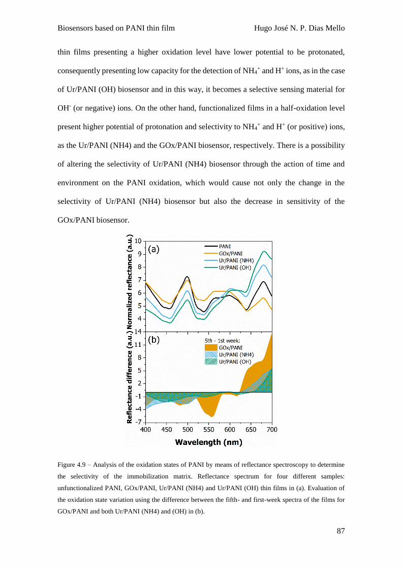
Biosensors based on PANI thin film Hugo José N. P. Dias Mello
87
thin films presenting a higher oxidation level have lower potential to be protonated,
consequently presenting low capacity for the detection of NH4+ and H+ ions, as in the case
of Ur/PANI (OH) biosensor and in this way, it becomes a selective sensing material for
OH- (or negative) ions. On the other hand, functionalized films in a half-oxidation level
present higher potential of protonation and selectivity to NH4+ and H+ (or positive) ions,
as the Ur/PANI (NH4) and the GOx/PANI biosensor, respectively. There is a possibility
of altering the selectivity of Ur/PANI (NH4) biosensor through the action of time and
environment on the PANI oxidation, which would cause not only the change in the
selectivity of Ur/PANI (NH4) biosensor but also the decrease in sensitivity of the
GOx/PANI biosensor.
Figure 4.9 – Analysis of the oxidation states of PANI by means of reflectance spectroscopy to determine
the selectivity of the immobilization matrix. Reflectance spectrum for four different samples:
unfunctionalized PANI, GOx/PANI, Ur/PANI (NH4) and Ur/PANI (OH) thin films in (a). Evaluation of
the oxidation state variation using the difference between the fifth- and first-week spectra of the films for
GOx/PANI and both Ur/PANI (NH4) and (OH) in (b).

Biosensors based on PANI thin film Hugo José N. P. Dias Mello
88
The evaluation of the oxidation state variation of the functionalized PANI thin
film through the analysis of the reflectance spectra is shown in Figure 4.9 (b) for the
GOx/PANI and for both Ur/PANI (NH4) and (OH) biosensors using the difference
between the spectra of the films for the fifth- and first-week experiments. A general
behaviour of the three functionalized PANI thin films is the increase in reflectance
intensity between 600 and 700 nm, approximately, and reduction of the reflectance
intensity between 400 and 550 nm, approximately. This behaviour, as discussed before,
is characteristic of thin films of PANI that change to a state of greater oxidation. This
corroborates the loss of sensitivity to glucose, maintenance of sensitivity to urea for a
biosensor with selectivity to hydroxyl ions, Ur/PANI (OH), and alteration of the
selectivity to urea for a biosensor initially selective to ammonium ions, Ur/PANI (NH4).
4.2.5. Partial conclusion
Rapidly and easily fabricated glucose and urea biosensors using the one-step
electrochemical immobilization technique by galvanostatic method to entrap glucose
oxidase and urease in PANI immobilization matrix presented changeable selectivity.
Functionalized PANI thin films were used as recognition stage connected to a
potentiometric transducer stage based on the IA-EGFET system, originating the EnFET
biosensor. The enzymatic biosensors presented similar sensitivity to other reported
devices, with a much simpler and faster fabrication method and a broad detection range.
The time evolution analysis of stability and repeatability showed that the glucose
biosensor response presented a fast decline, that the urea biosensor selective to hydroxyl
ions could maintain its proper function over all the tested period and that the ammonium
selective urea biosensor presented a changeable selectivity with sensitivity recovery after
change of selectivity from ammonium to hydroxyl ions. The characteristics of the
biosensor depended on the enzyme behaviour and mainly on the oxidation variation of

Biosensors based on PANI thin film Hugo José N. P. Dias Mello
89
the PANI immobilization matrix, which was responsible to the selectivity variation of
Ur/PANI (NH4) biosensor and great functionality loss of GOx/PANI biosensor. The
EnFET system is reliable and the functionalized thin films can be easily produced with
controllable selectivity.
4.3. PANI based optical and conductometric biosensor
In this section, the results obtained for the functionalized PANI based optical and
conductometric biosensor, regarding their calibration curve, sensitivity, linearity and
stability are presented.
4.3.1. Analysis of optical biosensor
The study of optical biosensors by reflectance spectroscopy is initiated by the analysis of
the spectral response curves as a function of the analyte concentration, followed by its
calibration curve, from which we extracted the sensitivity and linearity. These graphs are
shown in Figure 4.10. The spectral response for the GOx/PANI biosensor is shown in
Figure 4.10 (a). The inset graph shows the a* value as function of the glucose
concentration. The typical reflectance spectra for GOx/PANI biosensors presents a valley
around 450, 525 and 650 nm, and a peak around 500, 550, 600 and 680 nm. The sensing
behaviour of this system can be explored when focusing in the spectral region between
640 and 700 nm, the red band, approximately, which change proportionally to the glucose
concentration in solution, decreasing with the increasing in the glucose concentration.
This is explained by the working principle of enzymatically biosensors using PANI as
immobilization matrix [48], discussed previously.
Based on equation (10), increasing the glucose concentration causes an decrease
in the local pH, to a more acid environment, which causes a decrease in the spectral peak
at the described band for electrochemical produced PANI thin films [53]. This process,

Biosensors based on PANI thin film Hugo José N. P. Dias Mello
90
caused by polymer protonation/deprotonation of the PANI structure, also leads to a
change to greenish colour of the polymer, reversibly [15,94], and this can be verified by
the variation of the a* parameter, when changing to negative values, which indicates a
change to green colour, with increasing glucose concentration. Important to note that the
b* colour parameter remains practically constant for all the glucose range.
Figure 4.10 – Spectral response curves as a function of the analyte concentration for the glucose and urea
biosensors, and their calibration curves. The spectral response for the GOx/PANI biosensor in (a) and the
spectral response for the Ur/PANI biosensor in (b). The inset in both graphs shows the a* CIE colour
parameter. The calibration curve and indication of the sensitivity and linearity from GOx/PANI and
Ur/PANI biosensors in (c).

Biosensors based on PANI thin film Hugo José N. P. Dias Mello
91
The spectral response for the Ur/PANI biosensor is shown in Figure 4.10 (b). The
inset graph shows the a* value as function of the urea concentration. The typical
reflectance spectra for Ur/PANI biosensors presents a valley around 450, 530 and 650
nm, and a peak around 500, 550, 600 and 680 nm, just like for GOx/PANI. This is
expected once that the polymer’s properties due not depend on the enzyme and we
basically have the same immobilization matrix material. The sensing behaviour of this
system can all be explored focusing in the red band, between 640 and 700 nm,
approximately, which change proportionally to the urea concentration in solution,
decreasing with increasing urea concentration. Again, this is explained by the working
principle of enzymatically biosensors using PANI as immobilization matrix, but in this
case, we are interested in the hydrolytic urea catalysis by urease to ammonium, hydroxyl
ion and bicarbonate ions, as presented in equation (11).
Once the behaviour presented to the reflectance spectra of PANI thin films is
characteristic of protonation of its structure (decreasing intensity of the 680 nm peak with
increasing bio-analyte concentration), it can be conclude that the PANI immobilization
matrix acts as an ion-selective material detecting the ammonium ion, as shown by Zhybak
and colleagues [126]. Again, the a* colour parameter changes toward to a more greenish
colour. However, one difference between the biosensors made using glucose oxidase and
urease is the intensity response level of the reflectance spectra and a* colour parameter
and, although the structure-property relationship of the immobilization matrix material is
similar for both sensors, some characteristics are not the same but do not affect the sensor
behaviour.
The calibration curve for the optical biosensors was built using the integrated
reflectance in the range from 640 to 700 nm, once that this is the representative region of
the changes of the PANI thin films for these biosensors, to more precisely describe the

Biosensors based on PANI thin film Hugo José N. P. Dias Mello
92
changes in the thin films. Figure 4.10 (c) shows the calibration curve and indicates the
sensitivity and linearity of the GOx/PANI and Ur/PANI biosensors. The GOx/PANI
biosensor presented sensitivity of 2.5 ± 0.4 IR/decade and linearity of 99.1 % in the
concentration range between 10-1 and 10-5 mol/L of glucose. Optical biosensors are an
alternative for glucose monitoring, as can be seen by the proper working of the reflectance
biosensor presented here. In the literature, fluorescence glucose biosensors are also used
as an alternative to conventional biosensors. These are very specific but require embedded
probes [133]. The work of Russell and co-workers [134] and Yang and co-workers [111]
bring glucose biosensors by fluorescence, but they work for a narrower range of
concentration. The Ur/PANI biosensor presented a sensitivity of 8.9 ± 1.1 IR/decade and
linearity of 97.4 % for the entire concentration range, from 10-1 to 10-6 mol/L urea. In the
literature it is possible to find examples of urea optical biosensors as an alternative to
conventional biosensors. In addition, Alqasaimeh and co-workers [135] bring an optical
urea biosensor based on urease immobilized on silicon dioxide nanoparticles, SiO2NP,
whose production is complex, time-consuming (longer than 24 hours of preparation) and
requires adverse conditions. In addition, the optical urea biosensor demonstrated requires
more complex instrumentation, such as a computer to record the experimental data and
working linearly in the range from 10-3 to 10-1 mol/L, with linearity of 96 %.
4.3.2. Stability of the optical biosensor
The stability of biosensors, aiming their long-term use, is an important feature of these
devices, although it finds several causes to worsen it, like inactivation of the enzyme,
detachment from the immobilization matrix, among others [136]. Other factors related to
the immobilization matrix may also affect the long-term behaviour of biosensors,
decreasing their sensitivity and/or linearity, as reduction and oxidation when using
conducting polymers [137]. The stability, evolution over five weeks, of the sensitivity

Biosensors based on PANI thin film Hugo José N. P. Dias Mello
93
and linearity of GOx/PANI and Ur/PANI biosensors are shown in Figure 4.11 (a).
GOx/PANI biosensor loses its functionality rapidly, with a marked decrease in both
sensitivity and linearity, by the second week. The sensitivity starts at 2.5 IR/decade and
decays approximately 54% in the second week, reaching 1.2 IR/decade, then decreasing
to the lowest value, approximately 70%, in the fourth week, reaching 0.75 IR/decade.
Linearity also suffered a large decrease, of approximately 80 % in the second week,
making the use of the device unfeasible, and then declining by approximately 87 %,
reaching the minimum level of 12.7 % in the fifth week.
Figure 4.11 – The stability, evolution over five weeks, of the sensitivity and linearity of GOx/PANI and
Ur/PANI biosensors in (a). The stability of the a* CIE colour parameter of GOx/PANI and Ur/PANI
biosensors measured at concentration of 10-1 mol/L in (b) and (c), respectively.
Two factors are associated with the decrease in the functionality of the optical
glucose biosensor, the first being the release of enzymes from the polymer matrix, caused
by the functionalization method of PANI thin films, the one-step electrochemical
immobilization technique, which is responsible by the entrapment of enzymes in the
layers of electrochemically synthesized polymers [138]. Besides that, PANI sensitivity
and selectivity to ions depends on its oxidation state. Moreover, for the case of the optical
biosensor, we have that the oxidation process of the polymeric immobilization matrix

Biosensors based on PANI thin film Hugo José N. P. Dias Mello
94
over time, as previously discussed, changes its state to a more oxidized one where it loses
its ability to change colour when it protonates, different to what occur for PANI material
in a half-oxidized state [94].
The Ur/PANI biosensor also loses its functionality over the five weeks, as does
the GOx/PANI glucose biosensor. The sensitivity starts at 8.9 IR/decade and decays
approximately 98 % in the second week, reaching 0.1 IR/decade, which is the lowest
value reached by sensitivity over the five weeks. From this week on, the sensitivity
oscillates, going up and down till the fifth week. The fluctuations in the sensitivity values
are related to the total lack of coherence of the optical responses, being able to generate
results with little confidence. The linearity also suffers a great decrease, decreasing
approximately 75 % in the second week, going from 97 % to 24 %, which already makes
the use of the device unfeasible. Linearity still dropped 94 %, reaching its lowest value,
of 5.8 %, in the third week. Again, this behaviour is caused by the gradual oxidation of
the PANI thin film, acting as immobilization matrix and ion-detecting layer, that, as
previously discussed, unfeasible an optical response of the biosensor, causing loss of
sensitivity and linearity in the urea optical biosensor.
The stability of the a* CIE colour parameter of GOx/PANI and Ur/PANI
biosensors measured at concentration of 10-1 mol/L are shown in Figure 4.11 (b) and (c),
respectively. For both biosensors, the parameter changes to more positive values from the
first to the second week, indicating a change from more greenish to more reddish colour
of the PANI thin film which, as previously discussed, indicating a change to more
oxidized polymeric material. This reinforces the results showed and discussed, indicating
that a change in the oxidation state of the PANI thin films acting as immobilization matrix
and ion-detecting layer directly influences the sensitivity and linearity of enzymatic
optical biosensors.

Biosensors based on PANI thin film Hugo José N. P. Dias Mello
95
4.3.3. Analysis of conductometric biosensor
The study of conductometric biosensors is done by analysis of the curves of the raw and
fitted Nyquist diagram obtained by using the EIS data. These diagrams are shown in
Figure 4.12. The EIS curves for the glucose GOx/PANI and urea Ur/PANI biosensors are
shown in Figure 4.12 (a) and (b), respectively. Each spectrum was characterized using a
semicircle that intercepts the real impedance axis in a region of low and high frequency
and a region of diffusion. Figure 4.12 (a) and (b) show the original data as symbols, as
measured in the previously described system, and the curves obtained by adjusting the
Nyquist data by a computational analysis of the original data using the simplest equivalent
circuit usually used in systems composed by PANI [86].
Figure 4.12 – Raw data and fitted Nyquist diagram obtained by using the EIS technique. EIS curves for the
glucose GOx/PANI and urea Ur/PANI conductometric biosensors in (a) and (b), respectively.
The curve’s profile changed following the glucose and urea concentration.
Increasing the concentration of the bio-analyte causes a decrease in the semi-circle radius
for both systems. For the GOx/PANI biosensor the semi-circle profile is almost
completely shown while for the Ur/PANI biosensor the semi-circulus profile is partially
shown.
An equivalent circuit is a kinetic model provided by impedance techniques to
efficiently attribute a clear physical meaning to the parameters of interest, decoupling the

Biosensors based on PANI thin film Hugo José N. P. Dias Mello
96
electrochemical and mass-transport processes in the redox mechanisms of polymers
[139]. The simpler equivalent circuit applied to PANI based systems is shown in Figure
4.13 (a). In this circuit RS is the resistance of the solution and gives rise to the intercept
in the real axis in the region of high frequency. RF is the resistance of the film, the
resistance for charge transfer in the polymeric structure, and causes the interception in the
real axis in the region of low frequency. The film resistance is in parallel with the double-
layer capacitance, C, formed on the film surface. Based on this, on the Nyquist diagram
the urea conductometric biosensor has a higher resistance for charge transfer, i.e. a larger
semicircle in the diagram, than the glucose biosensor. This indicates that the impedance
of the urease functionalized PANI thin film is higher than for the glucose urease
functionalized PANI thin film when these systems are acting as sensors for their specific
analytes, urea and glucose, respectively. This difference may be related to the mobility of
ions that cause the protonation of the polymer matrix for each system. H+ ions possess
higher mobility than NH4+ ions, decreasing the impedance of the GOx/PANI system in
relation to Ur/PANI, as discussed by Segalini and co-workers [140].
As a consequence of the bio-sensing process, a decrease in the semi-circles radius
for both systems occurs, which characterizes, for both systems, a decrease of the
resistance for charge transfer, that is, variation in the system impedance, with the increase
of the analyte concentration, what was observed for other conductometric sensors using
EIS, for both glucose [141] and urea [107]. This effect is expected because the products
of the catalytic reactions of the enzymes are ions that cause the protonation of the PANI
matrix increasing its conductivity.

Biosensors based on PANI thin film Hugo José N. P. Dias Mello
97
Figure 4.13 – The simpler equivalent circuit applied to PANI based systems and used in this work in (a).
RS is the resistance of the solution, RF is the resistance of the film, the resistance for charge transfer in the
polymeric structure, and it is in parallel with the double-layer capacitance, C, formed on the film surface.
The calibration curves and indication of the sensitivity and linearity from GOx/PANI and Ur/PANI
biosensors in (b). The calibration curves based on the variation of the double-layer capacitance C and
solution impedance RS, in the inset, for the GOx/PANI and Ur/PANI biosensors in (c) and (d), respectively.
Through computational analysis of the raw data based on the equivalent circuit
the parameters of interest for the conductometric system can be obtained, in this case, the
resistance for charge transfer, the impedance of the biosensor. Using the obtained values,
the calibration curves are constructed for each biosensor. The calibration curves and
indication of the sensitivity and linearity from GOx/PANI and Ur/PANI biosensors are
shown in Figure 4.13 (b). The GOx/PANI biosensor presented sensitivity of 2.8 ± 0.3
RR/decade and linearity of 96.3 % in the concentration range from 10-1 to 10-5 mol/L of
glucose. The Ur/PANI biosensor presented sensitivity of 9.1 ± 1.6 RR/decade and
linearity of 99.2 % in the concentration range from 10-1 to 10-4 mol/L of urea. Comparing
these results to those obtained for optical biosensors by reflectance, a correlation between

Biosensors based on PANI thin film Hugo José N. P. Dias Mello
98
them can be verified. For the optical biosensors the sensitivity and linearity values for
GOx/PANI were 2.5 ± 0.4 IR/decade and 99.1 %, respectively, and for Ur/PANI were 8.9
± 1.1 IR/decade and 97.4 %, respectively. These data corroborate the understanding of
the structure-property relationship of conducting polymers, especially PANI, showing the
correlation between the optical and electrical properties through the same ratio between
the sensitivities for the two types of transduction system.
The stability analysis of the conductometric biosensors was impaired due to the
degradation of the samples during measurements in the following weeks. The
functionalized PANI thin films, working as immobilization matrix for the enzymes, were
detached from the substrate. However, the EIS technique is a rich and valuable method
of analysis. It provides information not only of the working electrode material, in this
case, the functionalized PANI thin films, but also on the system. The described
conductometric biosensor, based on the EIS technique using functionalized PANI thin
films with glucose oxidase and urease, was also analysed using the other electrochemical
parameters presented. The calibration curves based on the variation of the double-layer
capacitance C and solution impedance RS, in the inset, for the GOx/PANI and Ur/PANI
biosensors are shown in Figure 4.13 (c) and (d), respectively.
The double-layer capacitance value also decreases with increasing concentration
of analytes for both biosensors which is related due to an increase in the Debye length
[142]. From 10-6 to 10-4 mol/L there is practically no effect on the capacitance for the
GOx/PANI system, which decreases until 10-1 mol/L. In the Ur/PANI system the decrease
in the capacitance value occurs from 10-6 to 10-1 mol/L. The inserted graph shows that
there is practically no variation in the solution resistance as a function of glucose and urea
concentration, respectively, as expected once a buffer solution for analysis was used and

Biosensors based on PANI thin film Hugo José N. P. Dias Mello
99
neither the charge transfer process nor the ion movement process in the double layer alter
the mobile ion concentration in the solution.
The observed variations in the double-layer capacitance may be due to the
adsorption of ions, which change with the concentration of bio-analytes concentrations,
from the solution resulting in changes of the surface charge density and capacitance as
well as in the electric field distribution around the sensitive layer and electrode interface
[110]. The decreasing behaviour may be also due to an increase in the Debye length [142].
All the described process depends on the PANI thin films pore size and its behaviour in
solution, regarding mainly its swelling. Specifically, the PANI film swells more in dilute
solution compared to concentrated solutions. The swelling process increases the pore size
as well as accessibility of chargeable sites. Increase in the pore size reduces the double
layer interaction and hence increases the capacitance [143], indicating the process
observed in the described biosensor.
4.3.4. Partial conclusions
An optical biosensor based on reflectance spectroscopy and a conductometric biosensor
based on electrochemical impedance spectroscopy for sensing of glucose and urea were
produced using as bio-recognition stage a glucose oxidase and urease functionalized
PANI thin film obtained by the one-step electrochemical immobilization technique
applying the galvanostatic method. In this approach, the enzymes were entrapped in the
polymer which acted as immobilization matrix defining the biosensor working principle
to be based on the measurement of redox ions from the microenvironment of the enzyme.
The detection is based on the electrochromic variations in the PANI thin films when
sensing the products ions in solution of the enzymatic catalysis. These results corroborate
the understanding of the structure-property relationship of polyelectrochromic conducting
polymers showing the correlation between the optical and electrical properties. The

Biosensors based on PANI thin film Hugo José N. P. Dias Mello
100
optical biosensor stability depends on the PANI properties and its oxidation state besides
the detachment of the enzymes from the film. The EIS technique proved to be useful to
provides different information about the working electrode material useful to sensing
analysis, as the double-layer capacitance, and on the system.
4.4. Multimodal array of enzymatic biosensors (MAEB)
In this section, the use of the functionalized PANI thin films in a multiplexed system built
with a microcontroller PIC 16F628A, which is responsible for the time control and to
define which of the sensors of the input of the multiplexer must be connected to the output
is presented. The multiplexer used was the CD4052B which has two sets of four input
ports for a given output. The differential mode potentiometric transducer system, D-IA-
EGFET, is built with unit gain and used to improve the stability of the signal obtained
from the sensor.
4.4.1. pH effect on the MAEB
The effect of solution pH and REFET thin film in the MAEB system were tested to verify
the correct work of the system, once that the pH variations are crucial for biosensor
devices and the REFET stage can guarantees the sensor stability and decreases the
influence of environmental parameters. Figure 4.14shows the response of the MAEB
system with one glucose sensing film, GOx/PANI, one urea sensing film, Ur/PANI, and
one pH sensing film, the PANI sample. The measurements were done in a phosphate
buffer solution with pH 5.9 and 7.6.
The black circle data are related to the measurements done in solution with pH
5.9. In the aim of facilitate the visualization and interpretation of the data, three squares
were used to indicate, approximately, the sensor response level of each film in pH 5.9
(dark gray for GOx/PANI, medium gray for Ur/PANI and light gray for PANI). The

Biosensors based on PANI thin film Hugo José N. P. Dias Mello
101
glucose response was around 350 and 400 mV, for the urea biosensor the response was
around 300 and 350 mV and for the pH sensor the response was kept around 200 and 250
mV. Those values agree with typical values for this kind of biosensors and pH sensors.
Figure 4.14 – Measured data from the MAEB system with GOx/PANI, Ur/PANI, and pH sensing PANI
films, in two different pH buffer solution, 5.9 and 7.6. The three squares were used to indicate,
approximately, the sensor response level of each film in pH 5.9
The black open circle data are related to the measurements done in solution with
pH 7.9. In this case, we had the glucose response about 300 and 350 mV, for the urea
biosensor the response was about 250 and 300 mV and for the pH sensor the response
was about 100 and 150 mV. Again, those values also agree with typical values for this
kind of biosensors and pH sensors, as previously shown. The potentiometric response
variations of the MAEB system as function of solution pH and the distinction between
each specific biosensor indicates that the sensor can change its output due to the
environment and that the multiplex process occurs correctly.
4.4.2. REFET effect in the MAEB
Figure 4.15 shows the response of the MAEB and D-MAEB (Differential-MAEB)
systems with the same thin films as before, GOx/PANI, Ur/PANI and PANI. The REFET
sample was the copolymer PANI/PPY. As shown before, under specific polymerization

Biosensors based on PANI thin film Hugo José N. P. Dias Mello
102
conditions (strong acid aqueous medium), PPY decreases the pH sensitivity of PANI,
making it a good material for contrast films. The measurements occurred in phosphate
buffer solution with pH 5.9.
Figure 4.15 – Measured data from the MAEB (black circles) and D-MAEB (black open circles) systems
with the thin films of GOx/PANI, Ur/PANI and PANI in (a). The calibration curve of the copolymer
PANI/PPY-50/50 thin film in (b). The phosphate buffer solution pH’s was 5.9.
Figure 4.15 (a) shows the response of the MAEB system in both configurations.
The MAEB system shows the same response as before, also marked with three squares
in gray scale to indicate, approximately, the sensor response level of each film. However,
now we have the response for the D-MAEB system. In this case, the output voltage for
the glucose biosensor is about 150 to 200 mV, for the urea biosensor it is about 100 to
150 mV and for the pH sensor it is about 0 to 50 mV, along the 1800 s measurement. The

Biosensors based on PANI thin film Hugo José N. P. Dias Mello
103
decrease in the output voltage is due to the REFET present in the sensor. To check if the
decreasing potential is as expected, Figure 4.15 (b) shows the calibration curve of the
copolymer PANI/PPY-50/50 used as REFET. As we can see, for pH around 5.9, the
output is about 200 mV, exactly the correspondent value decreased in the response of the
films from the MAEB to the D-MAEB systems.
Figure 4.16 shows the response of the MAEB and D-MAEB systems with the
same thin films as before, GOx/PANI, Ur/PANI and PANI. The REFET sample was the
copolymer PANI/PPY. Now, the measurements occurred in phosphate buffer solution
with pH 7.6.
Figure 4.16 – Measured data for the MAEB (black circles) and D-MAEB (black open circles) systems with
the thin films of GOx/PANI, Ur/PANI and PANI using a phosphate buffer solution with pH 7.6.
Figure 4.16 shows the response of the MAEB system in both configurations using
another buffer solution, with pH 7.6. The differential sensor has its output voltage for the
glucose biosensor about 100 to 150 mV, for the urea biosensor it is about 100 to 150 mV
also and for the pH sensor it is about - 50 to 0 mV. The decrease in the output voltage is
due to the REFET present in the sensor. To check if the decease is as expected, Figure
4.15 (b) shows the calibration curve of the copolymer PANI/PPY-50/50 used as REFET.

Biosensors based on PANI thin film Hugo José N. P. Dias Mello
104
As we can see, for pH around 7.6, the output is about 150 mV, exactly the correspondent
value decreased in the response of the films from the MAEB to the D-MAEB systems.
4.4.3. Glucose and urea detection with MAEB
After previous tests with the system, the MAEB was used for the detection of the
biological analytes, glucose and urea. A selective response of the biosensors for each
target analyte and the indication of the solution’s pH using the PANI pH sensor thin film
were studied. Figure 4.17 shows the response for the D-MMBE system in phosphate
buffer solution pH 5.9, composed of GOx / PANI, Ur / PANI and the PANI pH sensor,
used to detect variations in the system related to the presence of glucose. Aiming for a
correct glucose detection, a pH solution between the two established levels was used,
closer to the optimum pH of the glucose oxidase enzyme. The REFET film used in the
contrast input of the transducer is the PANI/PPY-50/50 composite. During the
experiment, 1 mL of glucose in solution (0.5 mol/L) was injected in two moments, after
300 and 450 seconds of the beginning of the measurement.
Figure 4.17 – Response of the D-MAEB system composed of GOx/PANI and Ur / PANI biosensors, and
chemical pH sensor, the PANI thin film, to glucose injection in the phosphate buffer solution pH 5.9 of
measurement.

Biosensors based on PANI thin film Hugo José N. P. Dias Mello
105
The electrical potential levels for the D-MAEB device presented in the first 300
seconds of measurement are like those presented previously, that is, for the glucose
biosensor in the range of 150-200 mV, for the urea biosensor in the range 50 and 100 mV
and for the pH sensor, the PANI film maintained a response in the range between 0 and
50 mV. At the time of glucose injection into the system, we can clearly see the change in
the glucose biosensor response level, GOx/PANI, as expected, while the other sensors
remain virtually unchanged.
Figure 4.18, in turn, shows the response for the D-MAEB system in phosphate
buffer solution pH 7.6, composed of the same previously described sensing films,
GOx/PANI, Ur/PANI and PANI thin film for pH measurement, but now used to detect
variations in the system related to the presence of urea. Aiming for a correct urea
detection, a pH solution between the two established levels was used, closer to the
optimum pH of the urease enzyme. During the experiment, 1 mL of urea in solution (0.5
mol/L). was injected at two times, after 300 and 450 seconds of the beginning of the
measurement.
Figure 4.18 – Response of the D-MAEB system composed of GOx/PANI and Ur / PANI biosensors, and
chemical pH sensor, the PANI thin film, to urea injection in the phosphate buffer solution pH 7.6 of
measurement.

Biosensors based on PANI thin film Hugo José N. P. Dias Mello
106
Upon the injection of urea into the system, we can see the change in the level of
the urea biosensor response, Ur/PANI, as expected. However, for this experiment, the
glucose biosensor also responded to the presence of urea in solution, which may be related
to the fact that, although the immobilization of GOx enzyme over substrates improved its
stability, retaining its activity, the GOx denaturation by the presence of urea affect the
enzymatic conformational structure, which induces interactions between the analyte and
the bio-receptor [144].
4.4.4. Partial conclusions
The array system used to the simultaneous detection of glucose, urea and solution’s pH
showed to be useful. The MAEB by potentiometric transduction using a multiplexer
allowed one to use different thin film as sensing stage, being GOx/PANI, Ur/PANI and
PANI itself, controlling each one as the desired input in the correct moment. The system
showed good response to the variation in solution’s pH which varied between 5.9 to 7.6.
The variation of each film depends on its own pH`s sensitive. The system also showed
good response to the presence of a PANI/PPY thin film as REFET, changing the sensor
output level in 200 mV and 150 mV for pH 5.9 and 7.6, respectively. The biosensors
response maintained stable over 1800 s for both analyses, indicating to be useful to make
the simultaneous detection of several analytes. It was also able to detect the injection of
target analytes, glucose and urea, changing the electrical potential level of the specific
biosensor, proving to be a system able to measure multi analyte solutions.

EGOFET based biosensor Hugo José N. P. Dias Mello
107
5. EGOFET based biosensor
In this chapter, a combined study of poly(3-hexylthiophene) (P3HT)–based EGOFETs
using water as electrolyte and gated via a Pt gate wire electrode, regarding the proper
operational gate voltage window, as well as the effects of using a polymeric composite of
P3HT/poly (methyl methacrylate) (PMMA) as OSC layer in the EGOFET device is
presented. The effect of the distance between the active EGOFET pixel and the gate wire
on the device performance was also evaluated, considering the active layer material and
maximum gate voltage applied.
From the stable EGOFET device, an enzymatic biosensor for the detection of
glucose and urea using an EGOFET architecture where the gate electrode is selectively
functionalized with glucose oxidase (GOx) or urease (Ur), respectively, via grafting using
N-hydroxysuccinimide/1-ethyl-3-(3-dimethylaminopropyl) (NHS/EDC) chemistry onto
11-mercaptoundecanoic acid (MUA) modified gold wire gate electrodes is presented
[145,146]. The active channel was formed from poly(3-hexylthiophene) (P3HT), which
has previously shown stable performance in EGOFET devices using aqueous electrolyte
systems [147,148].
Figure 5.1 (a) depicts the schematic of a device with one functionalized gate
electrode for biosensor applications, showing the cross-section of the EGOEFT device
with a P3HT layer over the drain and source contacts, on top of the substrate. The
(modified) gate electrode is dipped in the electrolyte to complete the device structure. For
gate electrodes modified according to the reaction scheme in Figure 5.1 (b), the enzymatic
recognition/conversion of the analyte causes a combined effect on the device, a local
change to the electrochemical potential at device interfaces and changes in the
transconductance of the EGOFET due to redox reactions between the analyte and the bio-

EGOFET based biosensor Hugo José N. P. Dias Mello
108
recognition molecules which, in turn, affects the charge accumulation in the P3HT
channel – thereby yielding a detectable current response [149].
Figure 5.1 – The functionalization of the gate electrode of an EGOFET (showed in cross-section in a),
allows for the fabrication of biosensor for analytes such as urea or glucose. In (b), from left to right the
strategy for the enzyme immobilization onto carboxylate-terminated SAMs on Au gate rod is shown.
Starting with MUA-SAM linker, followed by the addition of NHS and the water soluble carbodiimide EDC
to the SAMs results in the formation of an NHS ester. Reaction of enzyme side-chain lysine residues with
the ester results in the formation of an amide bond.
OFETs based devices have proved to be excellent candidates as transducers for
detection of explosive molecules are crucial for our security as well as the environment
and human health [150–152]. 2,4,6-Trinitrotoluene (TNT) is not only one of the most-
known explosives but also a recognized pollutant for the environment present in air,
water, and soil. Due to its toxicity, the exposure of humans being to TNT can result in
severe adverse effects on human health, particularly targeting the circulatory system,
liver, spleen, and immune system [153]. Moreover, TNT and its products are mutagenic,
carcinogenic, and otherwise harmful to aquatic and terrestrial life [154]. To prevent the

EGOFET based biosensor Hugo José N. P. Dias Mello
109
consequences of human exposure to TNT, and other similar molecules, biological
monitoring for early detection is important and requires novel techniques [155].
The detection of TNT and its metabolites is achieved by several laboratory
techniques, such as high-performance liquid chromatography (HPLC), gas
chromatography-mass spectrometry (GC-MS), surface-enhanced Raman spectroscopy
(SERS), nuclear quadrupole resonance, ion mobility spectrometry, and other
spectroscopic methods [156,157], which are expense and sophisticated instruments or
requires complicated sample preparation processes. Lately, the scientific and
technological progress in the nano- and biotechnology fields allowed development of
techniques for TNT detection. It includes a laser device based on a semiconducting
organic polymer[158] and a dual nanosensor based on the reduction of TNT
electrochemically and consequent interaction of the products with conducting polymer
nanojunctions [159]. These new devices based on nano- and biotechnology are sensitive
with low detection limits. However, sensitive microelectronic devices suffer from false
positive responses when measuring a complex system which includes interfering analytes
or molecules with similar chemical structure, while many systems require multi-sample
analysis making the detection a time-consuming process.
Current sensing methods for TNT molecules are still far from fulling the
requirements of selectivity, sensitivity and real-time response. Improvements were made
in order to achieve a perfect match between the sensitivity, portability and real-time
response of microelectronic devices and the selectivity and reliability of biological
recognition. Dudhe et al. [160] presented a P3HT and CuII tetraphenylporphyrin
(CuTPP)-based OFET sensor applied as sensors for detection of vapours of nitro based
explosive compounds, TNT among them, making no use of specific targeting
bioreceptors for selectivity enhancement, while Surya et al. [161] presented an alternating

EGOFET based biosensor Hugo José N. P. Dias Mello
110
copolymer of thiophene flanked diketopyrrolopyrrole with thienylene-vinylenethienylene
(PDPP-TVT) based OFET applied as TNT sensor.
Tung et al. [162] developed a new generation of biosensors by introducing
evolutionary molecularly engineered peptide aptameric reagents as biorecognition
element onto Single Walled Carbon Nanotube-Field Effect Transistor (SWCNT-FET)
devices. They combined the high sensitivity of the SWNCT-FET transducer with binding
properties of the peptide aptamer to achieve the desirable selectivity. Berto et al. [163]
developed an EGOFET biosensor were the recognition units were surface immobilized
peptide aptamers instead of antibodies for tumour biomarkers. Kim et al. [164] produced
a TNT selective biosensors by combining TNT receptors bounded to conjugated
polydiacetylene (PDA) polymers with a SWCNT-FET device. The biosensor consists of
a TNT receptor made of a tripeptide (tryptophan-histidine-tryptophan: WHW),
discovered through phage display, linked to the conjugated polymer PDA, self-assemble
into vesicle structure, and then incubated on the SWCNT-FET surface. The device
presented real-time sensitivity and selectivity to other molecules with similar chemical
structure, specially the dinitrotoluene (DNT). An interesting example came from Wang
et al. [165] which make use of a TNT binding peptide for TNT detection based on a
maleimide-functionalized surface plasmon resonance (SPR) sensor.
A selective and sensitive bottom contact Electrolyte-Gated Organic Field Effect
Transistor (EGOFET), based on poly(3-hexylthiophene) (P3HT) as the organic
semiconducting layer, applied as TNT and DNT biosensor, with the receptors binding
peptides [166] (BP) for TNT and DNT coated onto the Au gate wire is presented. The
coated Au gate electrode is dipped in the electrolyte to complete the device structure. The
device’s selectivity is demonstrated with cross-analysis for TNT and DNT, using a
scramble binding peptide and with no binding peptide.

EGOFET based biosensor Hugo José N. P. Dias Mello
111
5.1. EGOFET based on P3HT
In this section, the development and testing of EGOFET devices based on P3HT layers is
described. Stability evaluation and gate-distance effects on the device were evaluated.
5.1.1. Methodology
5.1.1.1. Sample preparation
The EGOFET devices were fabricated using low-density prefabricated OFET test chips
(Ossila Ltd, Sheffield, UK) comprising a Si++/SiO2 (dox = 300 nm) substrate structured
with gold source, drain and gate electrodes (channel length L = 30 µm and channel width
W = 1 mm) having pre-fabricated octadecyltrichlorosilane/2,3,4,5,6-
pentafluorobenzenethiol (OTS/PFBT) layers on the SiO2/Au surfaces, respectively. The
substrates were cleaned by sonication method for five minutes in deionized (DI) water
and acetone. After drying under a flow of N2, the substrate was used immediately.
Regioregular poly(3-hexylthiophene) (P3HT) (Rieke Metals, Lincoln, Nebraska, USA,
MW = 37,000 g/mol, 98% regioregular) was deposited from a 5 mg/mL (0.5 wt.%)
chlorobenzene solution. For the composite films, 1 wt.% solutions of P3HT and poly
(methyl methacrylate) (PMMA) (Sigma Aldrich, MW = 120,000 g/mol) were prepared
by stirring for 5 minutes at 60 °C. Both solutions were mixed by stirring overnight (400
rpm) in a ratio of 3:7 P3HT/PMMA. All devices were deposited via spin-coating (1000
rpm, for 60 s) and annealed on a hot plate for 30 min at 120 °C, inside a N2 glovebox. DI-
water was used as electrolyte. A reservoir, which was made of polydimethylsiloxane
(PDMS, Sylgard 184) via a soft moulding process including a curing step overnight in
oven at 60 ºC was used to confine the electrolyte. The EGOFETs were gated via a
platinum (Pt) electrode.

EGOFET based biosensor Hugo José N. P. Dias Mello
112
5.1.1.2. EGOFET characterization
The electrical characterization was done using an Ossila multi-purpose probe station
adapted to the specific EGOFET architecture. Device testing was performed using a
Keithley 2636B Source-Measure Unit (SMU) controlled via LabView and measuring the
output and transfer characteristics of the devices.
5.1.2. EGOFET evaluation
The characterization of a field-effect transistor device, such as an EGOFET, is based on
the output characteristics (obtained by keeping the gate voltage constant and varying the
drain voltage only) and transfer characteristics (obtained by keeping the drain voltage
constant and varying the gate voltage only). From the output curves, the existence of a
field effect can be determined, as well as the presence and location of the linear and
saturation regimes. The saturation behaviour of the output characteristics in Figure 5.2
(a) for the P3HT-based EGOFET with DI water as electrolyte, gated via a Pt reference
electrode device demonstrate a good overall performance.
From the transfer curves it is possible to obtain information about the mobility µ,
on/off-current ratio and threshold voltage. Figure 5.2 (b) and (c) show the transfer curve
for the mentioned device. It presented on-current of about ~ 0.3 µA, with VDS = - 0.4 V
and VGS = - 0.3 V. The transfer curves of three devices are compared, exhibiting moderate
device-to-device variation, more pronounced for the off-current region (below VGS = 0.2
V). The on/off-current ratios for the transfer curves at VDS = -0.1 V are ~ 0.5 x 10² (on-
current: VGS = - 0.3 V, off-current: VGS = 0.4 V). In comparison, the on/off-current ratio
in the saturation regime showed a lower value of about ~ 0.3 x 10² due to an increased
leakage current, being responsible for the higher off-current.

EGOFET based biosensor Hugo José N. P. Dias Mello
113
Figure 5.2 – P3HT-based EGOFET device characterization. In (a) the output characteristics of three devices
(L ~ 30 µm and W ~ 1 mm) gated via DI water with a Pt gate wire. The gate voltage, VGS, varied from 0.1
to - 0.3 V in 0.1 V steps and the drain-source voltage, VDS, was swept from 0.0 to - 0.5 V. Transfer and
semilogarithmic transfer curves of three devices in the linear, VDS = - 0.1 V in (b), and saturation, VDS = -
0.4 V in (c), regimes. Semilogarithmic transfer curves of the source-drain currents in the left-axis and
source-gate current in the right-axis vs. gate voltage in (d), when different maximum gate voltages were
applied with fixed VDS = - 0.1 V.
Furthermore, the P3HT-based EGOFET device was not stable when tested with
higher gate voltages than VGS < -0.3 V. Aiming to obtain an operational stability, it is
important to choose a proper operational gate voltage window [167]. In this way, to
investigate the limits of the stable operation window and to demonstrate the device
degradation when exceeding operational potentials, P3HT-based EGOFETs gated via a
Pt electrode in DI water were tested with different maximum gate voltages applied. Figure
5.2 (d) depicts the corresponding transfer curves, obtained in the linear regime (VDS = -
0.1 V), with maximum gate voltages of 0.0, - 0.3, - 0.5 and - 0.6 V, sweeping from + 0.5
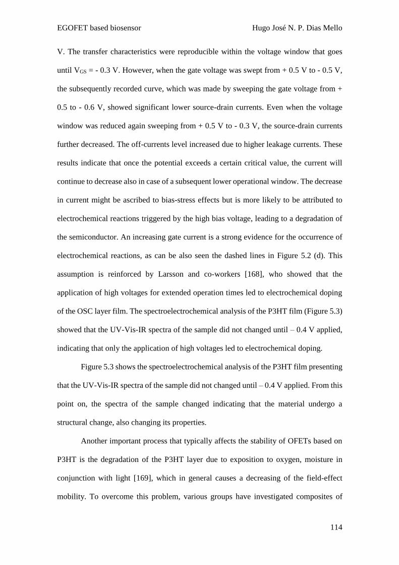
EGOFET based biosensor Hugo José N. P. Dias Mello
114
V. The transfer characteristics were reproducible within the voltage window that goes
until VGS = - 0.3 V. However, when the gate voltage was swept from + 0.5 V to - 0.5 V,
the subsequently recorded curve, which was made by sweeping the gate voltage from +
0.5 to - 0.6 V, showed significant lower source-drain currents. Even when the voltage
window was reduced again sweeping from + 0.5 V to - 0.3 V, the source-drain currents
further decreased. The off-currents level increased due to higher leakage currents. These
results indicate that once the potential exceeds a certain critical value, the current will
continue to decrease also in case of a subsequent lower operational window. The decrease
in current might be ascribed to bias-stress effects but is more likely to be attributed to
electrochemical reactions triggered by the high bias voltage, leading to a degradation of
the semiconductor. An increasing gate current is a strong evidence for the occurrence of
electrochemical reactions, as can be also seen the dashed lines in Figure 5.2 (d). This
assumption is reinforced by Larsson and co-workers [168], who showed that the
application of high voltages for extended operation times led to electrochemical doping
of the OSC layer film. The spectroelectrochemical analysis of the P3HT film (Figure 5.3)
showed that the UV-Vis-IR spectra of the sample did not changed until – 0.4 V applied,
indicating that only the application of high voltages led to electrochemical doping.
Figure 5.3 shows the spectroelectrochemical analysis of the P3HT film presenting
that the UV-Vis-IR spectra of the sample did not changed until – 0.4 V applied. From this
point on, the spectra of the sample changed indicating that the material undergo a
structural change, also changing its properties.
Another important process that typically affects the stability of OFETs based on
P3HT is the degradation of the P3HT layer due to exposition to oxygen, moisture in
conjunction with light [169], which in general causes a decreasing of the field-effect
mobility. To overcome this problem, various groups have investigated composites of

EGOFET based biosensor Hugo José N. P. Dias Mello
115
organic semiconductors (including P3HT) with polymer dielectrics, and indeed
composites of P3HT:PMMA have previously been shown to improve the overall device
stability, compared to pure P3HT films [170].
Figure 5.3 – Spectroelectrochemical analysis of the P3HT film with applied voltage from 0.05 to 1.0 V. For
each applied voltage the spectra of the sample were recorded to stablish a relationship between them.
Figure 5.4 (a) shows the output curves of EGOFET devices based on
P3HT/PMMA, showing saturation behaviour (as for the P3HT-based EGOFET) when
measured under the same experimental conditions (DI water as electrolyte, gated via a Pt
reference electrode).
The transfer curves of three devices are compared, exhibiting only a slight device-
to-device variation. Figure 5.4 (b) and (c) display the transfer curves for three composite-
based devices. The devices presented an on-current of about ~ 0.8 µA, with VDS = - 0.4
V and VGS = - 0.3 V. The off-current region is not completely reached for the operational
gate window VGS from + 0.5 to - 0.3 V, probably due to a variation in the device behaviour
when using the P3HT/PMMA composite. The on/off-current ratios for the transfer curves
at VDS= -0.1 V are ~ 0.5 x 10² (on-current: VGS = - 0.3 V, off-current: VGS = 0.5 V). In
comparison, the on/off-current ratio in the saturation regime showed a lower value of

EGOFET based biosensor Hugo José N. P. Dias Mello
116
about ~ 0.4 x 10² due to an increased leakage current, being responsible for the higher
off-current.
Figure 5.4 – A composite P3HT/PMMA (3:7 wt. ratio) - based EGOFET device characterization. In (a) the
output characteristics of one device (L ~ 30 µm and W ~ 1 mm) gated via DI water with a Pt gate wire. The
gate voltage, VGS, varied from 0.1 to - 0.3 V in a 0.1 V step and the drain-source voltage, VDS, varied from
0 to - 0.5 V. Transfer and semilogarithmic transfer curves of three devices in the linear, VDS = - 0.1 V in
(b), and saturation, VDS = - 0.4 V in (c), regime. Semilogarithmic transfer curves of the source-drain currents
in the left-axis and source-gate current in the right-axis vs. gate voltage in (d), when different maximum
gate voltages were applied with fixed VDS = - 0.1 V.
When comparing the overall performance of the EGOFETs using pure P3HT as
well as composite of 3:7 P3HT/PMMA it becomes evident, that the devices containing
the composite exhibit a 2.5 improvement of the on-current from ca. ~ 0.3 µA to ~ 0.8 µA
at comparable device settings (VDS = - 0.4 V and VGS = - 0.3 V). This may be related to
the field-effect mobility (µ) of holes, which is extracted from the transfer characteristics
in the linear regime. The mobility is estimated from the slope of the IDS vs. VGS curve. It

EGOFET based biosensor Hugo José N. P. Dias Mello
117
showed a value of 0.022 cm2/Vs for the pure P3HT based device and a value of 0.076
cm2/Vs for the composite. With a higher mobility, the correspondent EGOFET would
present a higher on-current. Also, the threshold voltage (VTH) presented a slight increase
for the composite, compared to the pure P3HT device, 0.14 to 0.11 V. This change toward
more positive values also contributes to an increase in the on-current of the device.
Furthermore, the P3HT/PMMA-based EGOFETs gated via a Pt electrode in DI
water were tested with different maximum gate voltages applied to evaluate the operation
window for stable device. Figure 5.4 (d) depicts the corresponding transfer curves, as for
the P3HT-based EGOFET. The transfer characteristics were reproducible within the
voltage window that goes until VGS ~ - 0.5 V. However, when the gate voltage was swept
from + 0.5 V to - 0.6 V, the source-drain currents diminished significantly. A moderate
improvement in the device reproducibility when compared to the P3HT-based EGOFET
(Figure 5.4 (c) compared to Figure 5.3 (c)), as well as an extension of the operating
window of the device to -0.5 V is shown. However, the use of the polymeric composite
does not add any substantial improvement to the stability of the device following
excessive gate voltages. Even though the voltage window was reduced again sweeping
from + 0.5 V to - 0.3 V, the source-drain currents further decreased. The off-currents level
increased due to higher leakage currents. These results are the same for the P3HT-based
EGOFET, also showing a possible electrochemical doping, even for a wider stable
operational window (VGS from + 0.5 to ~ - 0.5 V). The gate current also increased for
higher gate voltages, but if compared to the former device, the increasing in the gate
current for the maximum gate voltage VGS of – 0.3 V is lower, reinforcing the idea that
the composite material is a slightly more stable than the single component P3HT as
semiconductor layer.

EGOFET based biosensor Hugo José N. P. Dias Mello
118
To investigate the influence of the distance between the active EGOFET chip and
the gate wire, the device was evaluated with the Pt gate wire in four different positions
about the active chip. This study is important due to the geometric limitations on
biosensors design and other applications. Basically, the first chip is fixed for the
measurement of the drain current, IDS, while the gate wire position is changing. Figure
5.5 shows the source-drain current, IDS/IDS(max), ratio vs. distance between active
EGOFET chip and gate wire at a constant source-drain potential (VDS = - 0.1 V) and
varied maximum gate potential, one within the stable operational window (VGS = - 0.3)
and the other one out (VGS = - 0.5 V), for both materials used as OSC layer, P3HT and
P3HT/PMMA composite.
The analysis of the results indicated that the distance itself does not influence the
response of the device, at least over distance ranges >8 mm, and only the application of a
high voltage in the gate changes the response, but it occurs due to electrochemical
degradation, as previous discussed. When the final gate voltage remained constant at –
0.3 V, the drain current ratio varies by less than 20 % for the pure device, and less than
10 % for the composite, without any significant trend to lower values, supporting the
stability assessment. For the experiments performed by applying the final gate voltage of
– 0.5 V, there was a decrease of 50 and 70 %, respectively, for the P3HT and
P3HT/PMMA-based EGOFET, respectively. It seems, therefore, that the stable operating
window for the composite device is more like the pure film than suggested in Figure 5.4
(d), and the use of a composite with PMMA does not significantly retard electrochemical
doping, at least over prolonged testing. Nevertheless, the improved mobility and reduced
inter-device variance of the composite films suggest them to be a superior platform for
EGOFET devices, especially those based on aqueous dielectrics.

EGOFET based biosensor Hugo José N. P. Dias Mello
119
Figure 5.5 – Analysis of the ratio IDS/IDS(max) obtained from transfer curves of P3HT- and P3HT/PMMA-
based EGOFET gated via Pt wire in DI water applying a stable and non-stable maximum gate voltage, VGS
= - 0.3 and - 0.5 V, respectively, at four distances positions between the EGOFET device and Pt gate wire,
using a fixed VDS = - 0.1 V.
In summary, P3HT- and P3HT/PMMA-based EGOFETs gated in deionized water
via an Pt gate wire electrode, which exhibit a good overall performance with on-currents
up to 0.30 and 0.8 µA, respectively, were demonstrated. Due to the hydrophobic nature
of P3HT, the ion penetration and electrochemical reactions are negligible within a certain
window, however it was not possible to complete several measurements due to
irreversible degradation of the samples when this window was exceeded. The stability
problem was overcome with the proper maximum gate voltage range set and the use of
composite material P3HT/PMMA. The operation of the device with final gate voltage at
the maximum of ~ - 0.3 V for P3HT- and P3HT/PMMA-based EGOFET, did not allow
the electrochemical degradation. Evaluation of the device as function of the distance to
the gate wire showed that only the devices that were measured out of the proper
operational gate voltage window presented worsening of the response with increase in the
distance to the gate. These results reinforce the idea that the electrochemical degradation
occurs when not using the device in the proper operational voltage window. The choice

EGOFET based biosensor Hugo José N. P. Dias Mello
120
of a proper operational window is more important than the distance between the gate wire
and the EGOFET device for obtaining a stable device, allowing the use of the EGOFET
device other applications, such as bio- and ion-sensors.
5.2. P3HT based EGOFET enzymatic biosensor
In this section, the fabrication and application of a P3HT based EGOFET enzymatic
biosensor with Au gate electrode functionalized with GOx and Ur are described.
5.2.1. Sample preparation
Gate functionalization was achieved by immersing Au rods (ø = 1.0 mm, L = 25 mm) in
a 11-mercaptoundecanoic acid (MUA) ethanol solution (10 mmol/L) for 20 h [171]. After
rinsing and drying they were successively immersed in a 0.05 mol/L N-
hydroxysuccinimide (NHS) and 0.20 mol/L 1-ethyl-3-(3-dimethylaminopropyl (EDC)
DI-water solution for 1.5 h each [172]. Finally, the electrodes were immersed in a 10
mg/mL enzyme solution (GOx or Ur) in phosphate buffer solution (PBS, pH 7.4) for 1.5
h [173]. Upon removal from the solution, the rods were rinsed with PBS, dried and stored
at 4 ºC in a refrigerator when not in use. All transformations were carried out at room
temperature.
5.2.2. Biosensor evaluation
In a first step, the EGOFET performance was studied with the bare Au gate electrode and
the two modified Au gate rods: one functionalized with glucose-oxidase (GOx/Au), and
the other with urease (Ur/Au), using DI water as the gate dielectric. Figure 5.6 (a) shows
a comparison of the transfer curve in the linear regime from the three different gate
electrodes. A shift in threshold voltage is observed with gate functionalization. For the
bare-Au gate, the IDS current reaches approximately 0.06 µA at VGS = - 0.3 V in the linear

EGOFET based biosensor Hugo José N. P. Dias Mello
121
regime (VDS = - 0.1 V), while for the GOx and Ur modified gate, the IDS results
approximately 0.04 and 0.03 µA at VGS = - 0.3 V in the linear regime, respectively. For
both enzymatic modified gates an increase in the threshold voltage occurred. Such
variation in the threshold voltage may be elucidated by the surface coverage of the Au
electrodes by the enzymes, which change the electrical characteristics of the device.
Figure 5.6 – Transfer curves of P3HT transistors in the linear regime with three different gate electrodes:
The Au bare gate wire, the glucose-oxidase, GOx/Au, modified gate wire and the urease, Ur/Au, modified
gate wire in (a). Variation in the transfer curve in the linear regime, VDS = - 0.1 V, for the glucose biosensor,
GOx/Au, at glucose concentration varying from 10-6 to 10-3 mol/L and for DI-water.
To verify the device response to the analyte concentration, the transfer curves of
the GOx-modified device were measured for different concentrations of glucose in DI-
water. The concentration of glucose ranged from 10-6 to 10-1 mol/L. Figure 5.6 (b) shows
the evolution of the GOx-modified EGOFET transfer curves (in the linear regime), when

EGOFET based biosensor Hugo José N. P. Dias Mello
122
the measurement is carried out with increasing glucose concentration (from 10-6 to 10-1
mol/L, DI-water is also reported as reference). In the linear regime (VDS = - 0.1 V, fixed
in the VGS = - 0.3 V) the outputted IDS level for the glucose solution ranging from 10-6 to
10-3 mol/L changes from 0.03 µA to 0.04 µA. Equivalent results are obtained with the
urea biosensor, using the Ur-modified gate, in Figure 5.7. The variation in the IDS
indicates that the chemical reactions catalysed by absorption of the specific analytes by
the enzymes can change the electrode potential at the gate interface, hence causing a
variation in the drain-source current.
Figure 5.7 – Variation in the transfer curve in the linear regime, VDS = - 0.1 V, for the urea biosensor,
Ur/Au, at urea concentration varying from 10-6 to 10-3 mol/L and for DI-water.
From the devices’ transfer curve (measured in the linear regime), a calibration
curve for the glucose biosensor is obtained. The calibration curve is shown in Figure 5.8
(a) as relative variation of the drain current (ΔIDS/IDS = (IDS(solution) – IDS(DI-water))/
IDS(solution)) as a function of the glucose concentration (from 10-6 to 10-1 mol/L.. As
expected, the relative electrical response of the device using the bare-Au as gate is
negligible (black circles). For the GOx-modified gate, the relative drain current change is
linearly proportional to the logarithm of the glucose concentration between 10-6 and 10-3
mol/L. For concentration higher than 10-3 mol/L the change in electrical response

EGOFET based biosensor Hugo José N. P. Dias Mello
123
saturates. To investigate the device reversibility, a home-made fluid circuit was connected
to the PDMS reservoir to be able to change the analyte concentration during the
measurements via injection, while always keeping the gate immersed and the
semiconductor layer covered with electrolyte.
Figure 5.8 – In (a) the changing in the relative drain-source current (ΔIDS/IDS) of the EGOFET device for
the glucose biosensor, GOx/MUA/Au, at glucose concentration varying from 10-6 to 10-1 mol/L in the linear
regime, VDS = - 0.1 V, in a forward measurement protocol. The same response for the EGOEFT device for
the Au bare gate rods also shown. In (b) the reversibility analysis of the EGOFET based glucose biosensor.
The first five experiments were done with pure water, then with glucose at 10-4 mol/L and back to pure
water until the device recovered it previous response level.

EGOFET based biosensor Hugo José N. P. Dias Mello
124
When exposed to oxygen, P3HT does not remain stable. Especially when
combined with the presence of light, it leads to an increase in carrier concentration and
conductivity of the material, associated with a decrease in mobility by field effect, due to
the presence of scattering centres of carriers. The flow cell was necessary to yield
reversibility since without it, the devices underwent a rapid degradation [174,175]. First
the measurements were carried out in DI-water, then following the injection of a 10-4
mol/L glucose solution, and finally the measurements were repeated once the solution
was flushed with DI-water, and flushing was repeated until the current level returned to
its original level. Five measurements were made for each change in electrolyte solution.
Figure 5.8 (b) shows the results of this analysis for the GOx electrode system. The
GOx/Au system presented a reversible operating mode. This result is important since it
indicates that the system may be reused using differently functionalized gates for different
analyte detection.
The same experimental procedures were performed to test the urea biosensor, i.e.
the measurements were carried out with a P3HT based EGOFET device employing an
Ur-modified gate and variable urea concentrated solutions. Figure 5.9 (a) shows the
relative change in the drain-source current as function of the urea concentration. The
measurements were first carried out with the bare-Au gate which yielded no response to
changes in the urea concentration between 10-6 and 10-1 mol/L. As seen for the glucose
biosensor, the drain current level increases linearly with the logarithm of the analyte
concentration, and the saturation point is reached at 10-3 mol/L. The reversibility of the
urea biosensor was tested with the similar home-made setup used in the GOx-modified
EGOFET described above. The device was first measured in DI-water and showed a
consistent value of IDS with time, as shown in Figure 5.9 (b). Upon injection of the urea
solution (10-4 mol/L) the device showed an abrupt increase in IDS, demonstrating the
EGOFET based biosensor Hugo José N. P. Dias Mello
125
immediate electrical response as result of the absorption of urea to the enzyme. The
reservoir was then flushed with several cycles of DI-water. Unlike for the glucose sensor,
the decay in IDS was much slower following the flushing of the urea. However, with
repeated flushing, the device response showed a clear trend towards its original value.
Figure 5.9 – In (a) the changing in the relative drain-source current (ΔIDS/IDS) of the EGOFET device for
the urea biosensor, Ur/MUA/Au, at urea concentration varying from 10-6 to 10-1 mol/L in the linear regime,
VDS = - 0.1 V, in a forward measurement protocol. The same response for the EGOEFT device for the Au
bare gate is also shown. In (b) the reversibility analysis of the EGOFET based urea biosensor. The first five
experiments were done with pure water, then with urea at 10-4 mol/L and back to pure water for 4 times.
While the precise reason for this difference is not yet clear, one possibility is that
the smaller molecular weight of urea, compared to glucose results in faster diffusion

EGOFET based biosensor Hugo José N. P. Dias Mello
126
kinetics in the electrolyte solution, with the greater likelihood of back-flowing into the
PDMS reservoir. This theory is supported by the gradual increase in IDS following each
flushing cycle. This experimental limitation could be easily overcome by employing a
continuous liquid flow over the device.
To test the enzymatic selectivity of the functionalized gate electrode, the relative
drain-source current change (ΔIDS/IDS) was calculated for the GOx-modified Au gate and
the Ur-modified Au gate. First, the GOx/Au (Ur/Au) device was exposed to glucose
(urea), followed by water, then urea (glucose), and finally to water (analytes concentration
= 10-3 mol/L). Figure 5.10 displays the results of the measurements carried out with the
functionalized gates as well as for a reference bare-Au gate.
Figure 5.10 – Selectivity analysis of the EGOFET based enzyme modified biosensors with relative drain-
source (ΔIDS/IDS) of the device against glucose and urea analytes. The Au bare gate rod electrode was
measured for non-specific binding analysis.
For the GOx-modified gate the glucose analyte gives a high response
(approximately ΔIDS/IDS ~ 0.6). However, in the presence of urea, the device also shows
a modest increase in IDS (approximately ΔIDS/IDS ~ 0.25). Although the immobilization of
GOx enzyme over substrates improved its stability, retaining its activity, the GOx
denaturation by the presence of urea affect the enzymatic conformational structure, which
induces interactions between the analyte and the bio-receptor [144]. In the case of the Ur-

EGOFET based biosensor Hugo José N. P. Dias Mello
127
modified gate, the presence of urea showed a high response (approximately ΔIDS/IDS ~
0.45) but showed negligible change in the presence of the glucose analyte (approximately
ΔIDS/IDS ~ 0.0). These results indicate that both the proposed biosensors are selective
regarding cross analysis between glucose and urea, with the Ur-modified gate showing
almost perfect selectivity between these two analytes. In contrast, the bare Au gate
showed negligible change in IDS in the presence of either urea or glucose, showing that
the specificity of the biosensor came from the enzyme immobilized in the gate wire.
From the previous results, the coating of the enzymes in the Au gate rod was
successfully achieved, and thus enzymatic biosensors based on P3HT EGOFET devices
were realized. The change in analyte concentration generates a variation in the EGOFET
response. For both biosensors the linear range was from 10-6 to 10-3 mol/L, after which, a
saturation in the response was observed in both cases. To be a useful biosensor device,
reversibility should be observed, as was demonstrated for measurements with a 10-4
mol/L solution. It can be explained by variations in the gate potential level due to the
redox reactions occurring between the analyte and the bioreceptor influencing the
EGOFET current. This system represents a modular design, where one can change the
functionalized gate without any loss of functionality of the EGOFET, if the active channel
of the device remains intact and no chemical or electrochemical doping has occurred. The
devices studied here were for GOx-modified Au and Ur-modified Au gate electrodes. The
devices showed also cross selectivity to the target analyte, which is vital for its use in
combined and matrix systems.
5.3. P3HT based EGOFET TNT and DNT biosensor
In this section, the fabrication and application of a P3HT based EGOFET TNT and DNT
biosensor with Au gate electrode functionalized with specific binding peptides are
described.
EGOFET based biosensor Hugo José N. P. Dias Mello
128
5.3.1. Sample preparation
The gate functionalization was achieved by immersing Au rods (ø = 1.0 mm, L = 25 mm)
in a 1 mmol/L peptide solution (for the three peptides: scrambled, TNT and DNT binding
peptides) in deionized (DI) water for 24 h. Upon removal from the solution, the rods were
rinsed with DI-water, dried and stored at 4 ºC in a refrigerator when not in use. All
experiments were carried out at room temperature.
5.3.2. Biosensor evaluation
The EGOFET performance was studied with the bare Au gate electrode and the three
modified Au gate rods: one functionalized with TNT binding peptide (TNT-BP), with
DNT binding peptide (DNT-BP), and one with a scramble peptide (Scr-BP) using DI
water as the gate dielectric. Figure 5.11 (a) shows a comparison of the transfer curve in
the linear regime from the four different gate electrodes. A shift in threshold voltage and
a variation in the IDS current level are observed with gate functionalization. For the bare-
Au gate, the IDS current reaches approximately 0.11 µA at VGS = - 0.3 V in the linear
regime (VDS = - 0.1 V), while for the TNT and DNT binding peptides, the IDS result
approximately 0.20 µA at VGS = - 0.3 V in the linear regime, and for the scramble binding
peptide, the IDS downed to 0.05 µA at VGS = - 0.3 V in the linear regime. Variation in the
threshold voltage for the modified gate electrodes may be elucidated by the surface
coverage of the Au electrodes by the peptides, which change the electrical characteristics
of the device.
To verify the device response to the analyte concentration, the transfer curves of
the TNT-BP modified device were measured for different concentrations of TNT in
ethanol. The concentration of TNT ranged from 10-15 to 10-4 mol/L in the complete
experiment. Figure 5.11 (b) shows the evolution of the TNT-BP modified EGOFET

EGOFET based biosensor Hugo José N. P. Dias Mello
129
transfer curves (in the linear regime), when the measurement is carried out with increasing
TNT concentration from 10-15 to 10-6 mol/L, showing only few curves in order to make it
easy to see the variations. In the linear regime (VDS = - 0.1 V, fixed in the VGS = - 0.3 V)
the outputted IDS level for the TNT solution ranging from 10-15 to 10-6 mol/L changes
from 0.25 µA to 0.10 µA.
Figure 5.11 – Transfer curves of P3HT transistors in the linear regime with four different gate electrodes:
The Au bare gate wire, the TNT binding peptide, TNT-BP, the DNT binding peptide, DNT-BP, and the
scramble binding peptide, Scr-BP, modified gate wires in (a). Variation in the transfer curve in the linear
regime, VDS = - 0.1 V, for the TNT biosensor, TNT-BP, at TNT concentration varying from 10-15 to 10-6
mol/L, showing intercalated curves to a clear presentation in (b).
Equivalent results are obtained with the DNT biosensor, using the DNT-BP
modified gate. The variation in the IDS indicates that the chemical reactions occurring
between the specific binding peptide and the analytes can change the electrode potential
at the gate interface, hence causing a variation in the drain-source current.

EGOFET based biosensor Hugo José N. P. Dias Mello
130
From the devices’ transfer curve (measured in the linear regime), a calibration
curve, for both TNT and DNT biosensor, is obtained. The calibration curve of the TNT
biosensor is shown in Figure 5.12 (a) as relative variation of the drain current (ΔIDS/IDS =
(IDS(solution) – IDS(EtOH))/IDS(solution)) as a function of the TNT concentration (from
10-15 to 10-4 mol/L). For the TNT-BP modified gate, the relative drain current change is
linearly proportional to the logarithm of the TNT concentration between 10-10 and 10-8
mol/L, when doing a forward measurement. For concentration lower than 10-11 and higher
than 10-8 mol/L, the change in electrical response saturates. The gradual saturation in the
drain-source current was caused by the binding between the receptor domain of the
peptide and TNT.
For the DNT-BP modified gate, shown in Figure 5.12 (b), the relative variation of
the drain current is linearly proportional as function of DNT concentration, ranging from
10-6 to 10-4 mol/L. As observed for the TNT-BP biosensor, the increased current of the
biosensor can be explained by the chemical gating effects caused by binding of the
analyte, DNT, to the specific binding peptide, DNT-BP, which induce electrical changes
in the EGOFET device. Both biosensors presented a back measurement which maintain
the relative current response constant in the saturation current level, approximately 0.55
µA and 0.35 µA to TNT-BP and DNT-BP biosensors, respectively (open circles). This
behaviour may be explained by a binding process between the target analyte, TNT or
DNT, and the peptides which saturates the receptors after a specific concentration level.
The specificity of the biosensor toward interfering molecules was tested by
experiments using compounds of similar chemical structures, i.e., a cross-selectivity
analysis where the TNT-BP biosensor measured DNT analytes and vice-versa. The
selectivity of the biosensor was tested by experiments using a non-modified gate

EGOFET based biosensor Hugo José N. P. Dias Mello
131
electrode, using bare Au rods, and using a scramble binding peptide (Scr-BP) to analyse
TNT and DNT solutions.
Figure 5.12 – The changing in the relative drain-source current (ΔIDS/IDS) of the EGOFET device for the
TNT biosensor, TNT-BP, at TNT concentration varying from 10-15 to 10-4 mol/L, in (a), and for the DNT
biosensor, DNT-BP, at DNT concentration varying from 10-6 to 10-4 mol/L, in (b), in the linear regime, VDS
= - 0.1 V, in a forward and back measurement protocol.
For both analyses, the relative drain-source current change (ΔIDS/IDS) was
calculated. First, the ΔIDS/IDS of TNT-BP and DNT-BP devices was obtained from the
calibration curve at 10-6 mol/L to the specific analyte, TNT and DNT, respectively. Then,
both systems were exposed to the cross-target analyte, TNT and DNT for the DNT-BP
and TNT-BP biosensor, respectively, in the concentration range from 10-6 to 10-4 mol/L
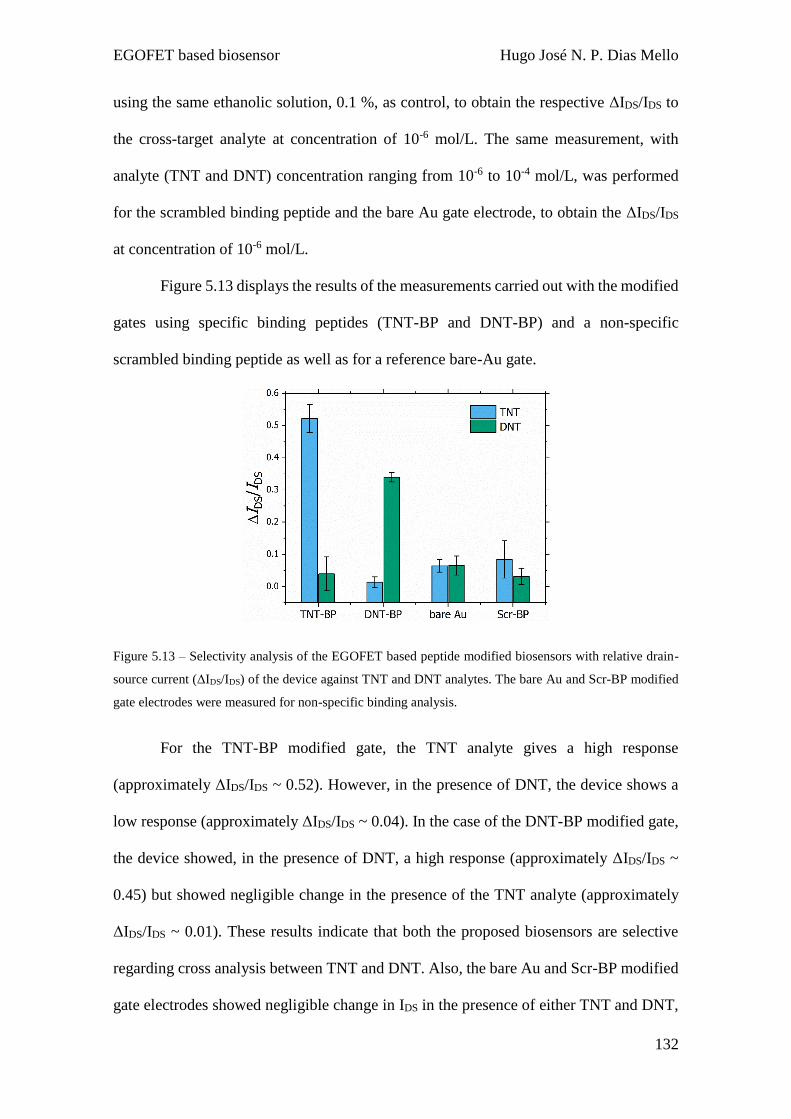
EGOFET based biosensor Hugo José N. P. Dias Mello
132
using the same ethanolic solution, 0.1 %, as control, to obtain the respective ΔIDS/IDS to
the cross-target analyte at concentration of 10-6 mol/L. The same measurement, with
analyte (TNT and DNT) concentration ranging from 10-6 to 10-4 mol/L, was performed
for the scrambled binding peptide and the bare Au gate electrode, to obtain the ΔIDS/IDS
at concentration of 10-6 mol/L.
Figure 5.13 displays the results of the measurements carried out with the modified
gates using specific binding peptides (TNT-BP and DNT-BP) and a non-specific
scrambled binding peptide as well as for a reference bare-Au gate.
Figure 5.13 – Selectivity analysis of the EGOFET based peptide modified biosensors with relative drain-
source current (ΔIDS/IDS) of the device against TNT and DNT analytes. The bare Au and Scr-BP modified
gate electrodes were measured for non-specific binding analysis.
For the TNT-BP modified gate, the TNT analyte gives a high response
(approximately ΔIDS/IDS ~ 0.52). However, in the presence of DNT, the device shows a
low response (approximately ΔIDS/IDS ~ 0.04). In the case of the DNT-BP modified gate,
the device showed, in the presence of DNT, a high response (approximately ΔIDS/IDS ~
0.45) but showed negligible change in the presence of the TNT analyte (approximately
ΔIDS/IDS ~ 0.01). These results indicate that both the proposed biosensors are selective
regarding cross analysis between TNT and DNT. Also, the bare Au and Scr-BP modified
gate electrodes showed negligible change in IDS in the presence of either TNT and DNT,

EGOFET based biosensor Hugo José N. P. Dias Mello
133
showing that the specificity of the biosensor came from the binding peptide coating in the
gate wire.
In summary, a rapid, sensitive and selective TNT and DNT biosensor through the
combination of P3HT-based EGOFET and specific receptor binding peptides was
developed. The change in analyte concentration generates a variation in the EGOFET
response. For the TNT biosensor the linear range was from 10-11 to 10-8 mol/L, after
which, a saturation in the response was observed. For the DNT biosensor, the linear range
was from 10-6 to 10-4 mol/L. The device’s working can be explained by variations in the
gate potential level due to chemical binding occurring between the analyte and the
bioreceptor, the receptor peptides, influencing the EGOFET current. This system
represents a modular design, where one can change the functionalized gate without any
loss of functionality of the EGOFET, if the active channel of the device remains intact
and no chemical or electrochemical doping has occurred. The devices studied here were
for TNT-BP modified Au and DNT-BP modified Au gate electrodes, and another device
based on a scrambled peptide, Scr-BP, was tested, along with a bare Au rod, to investigate
the selectivity of the biosensor, which is vital for its use in combined and matrix systems.

Conclusions Hugo José N. P. Dias Mello
134
6. Conclusions
Solid-state biosensors based on field-effect transistors transducer and organic
semiconducting materials were developed. The biosensors developed were used to detect
biomedical and health interest target analytes such glucose, urea, and TNT/DNT. The
devices’ architecture is based on the use of semiconducting polymers in the FET
structures. Two kinds of devices were presented, the EGFET and the EGOFET, using
PANI and P3HT, respectively, allied to the use of immobilized bio-sensing elements,
such as enzyme and binding peptides.
First, the structure-property relationship of PANI thin films fabricated through the
galvanostatic electrodeposition technique, analysing the influence of the
electrodeposition parameters on film’s properties, characteristics and response as pH
sensor was done. The influence of deposition parameters such as current density,
deposition time, aniline monomer concentration, as well as the use of polymeric
composites, with polypyrrole was studied . Beyond the potentiometric pH EGFET sensor,
the PANI thin films were applied on optochemical pH sensors due to their electrochromic
behaviour. The optochemical sensor measures the change in some optical parameter of
the chemically-sensitive film after its exposure to the target analyte. This study provides
us with information about the PANI thin films and the transducer system, EGFET, for the
further development of PANI based EnFET biosensor.
Glucose and urea biosensors using the one-step electrochemical immobilization
technique by galvanostatic method to entrap glucose oxidase and urease in PANI
immobilization matrix were achieved. Functionalized PANI thin films were used as
recognition stage connected to an EGFET system, originating the EnFET biosensor. The
characteristics of the biosensor depended on the enzyme behaviour and mainly on the
oxidation variation of the PANI immobilization matrix, which was responsible for the

Conclusions Hugo José N. P. Dias Mello
135
sensitivity, linearity and selectivity of the biosensors. The EnFET system is reliable and
the functionalized thin films can be easily produced with controllable selectivity.
The same functionalized PANI thin films were used in the development of an
optical biosensor based on reflectance spectroscopy and a conductometric biosensor
based on electrochemical impedance spectroscopy. These biosensors worked measuring
the redox ions from the microenvironment of the enzyme. The detection is based on the
electrochromic variations in the PANI thin films when sensing the such ions from the
enzymatic catalysis of the analytes. These results corroborate the understanding of the
structure-property relationship of polyelectrochromic conducting polymers showing the
correlation between the optical and electrical properties. The optical biosensor stability
depends on the PANI properties and its oxidation state besides the detachment of the
enzymes from the film. The EIS technique proved to be useful to provides different
information about the working electrode material useful to sensing analysis, as the
double-layer capacitance, and on the system.
In order to be able to measure different target analytes simultaneous from the same
sample, an array system of enzymatic biosensors was built. The multimodal array of
enzymatic biosensors based on potentiometric transduction using a multiplexer allowed
one to use different thin film as sensing stage. One system with glucose and urea
biosensor based on functionalized PANI thin films and a pH sensor based on a PANI thin
film was tested. The system showed good response to the variation in solution’s pH,
worked properly with a PANI/PPY REFET film in the contrast input of the device and it
was also able to detect the injection of target analytes, glucose and urea, changing the
electrical potential level of the specific biosensor, proving to be a system able to measure
multi analyte solutions.

Conclusions Hugo José N. P. Dias Mello
136
Based on the same principle of using organic semiconducting materials in FET
based sensors, an EGOFET device with P3HT layer was built to be used as biosensor.
Initially, P3HT thin films were used as OSC layer on EGOFET devices. To overcome the
degradation of the device, the stability problem was evaluated with maximum gate
voltage range and composite material P3HT/PMMA testing. The operation of the device
with final gate voltage at the maximum of – 0.4 V, approximately, did not allow the
electrochemical degradation. Evaluation of EGOFET parameters as function of distance
between active device and gate wire reinforce the idea that the electrochemical
degradation occurs when not using the device in the proper operational voltage window.
The conclusion that the distance between the measured chip and the gate wire does not
influence the EGOFET device may be used in the biosensor applications.
For the biosensor application, modified Au gate wires by coating of enzymes,
glucose-oxidase and urease, were produced, for use in the enzymatic biosensor and by
coating of TNT and DNT specific peptides. In the first case, the procedure is based on the
SAM of MUA coating followed by activation by EDC and NHS solution and finally, the
glucose oxidase and urease coating. The change in analyte concentration generates a
variation in the EGOFET response. It can be explained by variations in the gate potential
level due to the redox reactions occurring between the analyte and the bioreceptor
influencing the EGOFET current. All the devices presented selectivity and sensitivity to
the specific analyte.
Promising results have been achieved from the study of biosensors based on
organic semiconducting polymers. The FET transduction system proved to be an
excellent platform for biosensors development, as well as the techniques of
functionalization of the samples to be used in the biosensors. The study presented in this
thesis opened new possibilities of detection and devices architecture for the future.

List of publication Hugo José N. P. Dias Mello
137
List of publication
This thesis is mainly based on work that has been published within the journals mentioned
below. The author of this thesis is also the first author of the listed publications and wrote
the manuscripts, unless otherwise noted.
[1] H.J.N.P.D. Mello, M. Mulato, Effect of aniline monomer concentration on
PANI electropolymerization process and its influence for applications in chemical
sensors, Synth. Met. 239 (2018) 66–70. doi:10.1016/j.synthmet.2018.02.008.
[2] H.J.N.P.D. Mello, M. Mulato, Influence of galvanostatic electrodeposition
parameters on the structure-property relationships of polyaniline thin films and
their use as potentiometric and optical pH sensors, Thin Solid Films. 656 (2018) 14–
21. doi:10.1016/j.tsf.2018.04.022.
[3] H.J.N.P.D. Mello, M. Mulato, PANI/PPY blend thin films electrodeposited for
use in EGFET sensors, J. Appl. Polym. Sci. 135 (2018) 46625. doi:10.1002/app.46625.
[4] H.J.N.P.D. Mello, F.M. Mano, M. Mulato, A multimodal array of enzymatic
biosensors: Effect of solution’s pH and REFET film, in: 2017 32nd Symp.
Microelectron. Technol. Devices SBMicro, 2017: pp. 1–4.
doi:10.1109/SBMicro.2017.8113029.
[5] H.J.N.P.D. Mello, S. Dalgleish, G. Ligorio, M. Mulato, E.J.W. List-Kratochvil,
Stability evaluation and gate-distance effects on electrolyte-gated organic field-
effect transistor based on organic semiconductors, in: Org. Hybrid Sens. Bioelectron.
XI, International Society for Optics and Photonics, 2018: p. 1073819.
doi:10.1117/12.2322665.

References Hugo José N. P. Dias Mello
138
References
[1] L.C. Clark, C. Lyons, Electrode systems for continuous monitoring in
cardiovascular surgery, Ann. N. Y. Acad. Sci. 102 (1962) 29–45.
[2] P. Bergveld, Development of an Ion-Sensitive Solid-State Device for
Neurophysiological Measurements, IEEE Transactions on Biomedical
Engineering. BME-17 (1970) 70–71. doi:10.1109/TBME.1970.4502688.
[3] K. Rahimi, I. Botiz, J. O. Agumba, S. Motamen, N. Stingelin, G. Reiter, Light
absorption of poly(3-hexylthiophene) single crystals, RSC Advances. 4 (2014)
11121–11123. doi:10.1039/C3RA47064D.
[4] T. Lindfors, A. Ivaska, pH sensitivity of polyaniline and its substituted derivatives,
Journal of Electroanalytical Chemistry. 531 (2002) 43–52. doi:10.1016/S0022-
0728(02)01005-7.
[5] L. He, Y. Jia, F. Meng, M. Li, J. Liu, Gas sensors for ammonia detection based on
polyaniline-coated multi-wall carbon nanotubes, Materials Science and
Engineering: B. 163 (2009) 76–81. doi:10.1016/j.mseb.2009.05.009.
[6] X. Fu, C. Jia, Z. Wan, X. Weng, J. Xie, L. Deng, Hybrid electrochromic film based
on polyaniline and TiO2 nanorods array, Organic Electronics. 15 (2014) 2702–
2709. doi:10.1016/j.orgel.2014.07.040.
[7] Z. Ping, B.G.E. Nauer, H. Neugebauer, J. Theiner, A. Neckel, Protonation and
electrochemical redox doping processes of polyaniline in aqueous solutions:
Investigations using in-situ FTIR-ATR spectroscopy and a new doping system, J.
Chem. Soc., Faraday Trans. 93 (1997) 121–129. doi:10.1039/A604620G.
[8] A.G. MacDiarmid, A.J. Epstein, Polyanilines: a novel class of conducting
polymers, Faraday Discuss. Chem. Soc. 88 (1989) 317–332.
doi:10.1039/DC9898800317.
References Hugo José N. P. Dias Mello
139
[9] A.G. MacDiarmid, Synthetic Metals: A Novel Role for Organic Polymers,
Angewandte Chemie International Edition. 40 (2001) 2581–2590.
doi:10.1002/1521-3773(20010716)40:14<2581::AID-ANIE2581>3.0.CO;2-2.
[10] U. Lange, N.V. Roznyatovskaya, V.M. Mirsky, Conducting polymers in chemical
sensors and arrays, Analytica Chimica Acta. 614 (2008) 1–26.
doi:10.1016/j.aca.2008.02.068.
[11] J.L. Bredas, G.B. Street, Polarons, bipolarons, and solitons in conducting
polymers, Acc. Chem. Res. 18 (1985) 309–315. doi:10.1021/ar00118a005.
[12] A. Kitani, J. Izumi, J. Yano, Y. Hiromoto, K. Sasaki, Basic behaviors and
properties of the electrodeposited polyaniline., Bulletin of the Chemical Society of
Japan. 57 (1984) 2254–2257.
[13] D. Zhang, Y. Wang, Synthesis and applications of one-dimensional nano-
structured polyaniline: An overview, Materials Science and Engineering: B. 134
(2006) 9–19. doi:10.1016/j.mseb.2006.07.037.
[14] Q. Chang, K. Zhao, X. Chen, M. Li, J. Liu, Preparation of
gold/polyaniline/multiwall carbon nanotube nanocomposites and application in
ammonia gas detection, J Mater Sci. 43 (2008) 5861–5866. doi:10.1007/s10853-
008-2827-3.
[15] T. Kobayashi, H. Yoneyama, H. Tamura, Electrochemical reactions concerned
with electrochromism of polyaniline film-coated electrodes, Journal of
Electroanalytical Chemistry and Interfacial Electrochemistry. 177 (1984) 281–291.
doi:10.1016/0022-0728(84)80229-6.
[16] J. Huang, R.B. Kaner, A General Chemical Route to Polyaniline Nanofibers, J.
Am. Chem. Soc. 126 (2004) 851–855. doi:10.1021/ja0371754.

References Hugo José N. P. Dias Mello
140
[17] E.M. Genies, C. Tsintavis, Redox mechanism and electrochemical behaviour or
polyaniline deposits, Journal of Electroanalytical Chemistry and Interfacial
Electrochemistry. 195 (1985) 109–128. doi:10.1016/0022-0728(85)80009-7.
[18] S. Bhadra, D. Khastgir, N.K. Singha, J.H. Lee, Progress in preparation, processing
and applications of polyaniline, Progress in Polymer Science. 34 (2009) 783–810.
doi:10.1016/j.progpolymsci.2009.04.003.
[19] L. Valentini, M. Cardinali, M. Grkovic, P.S. Uskokovic, F. Alimenti, L. Roselli,
J.M. Kenny, Flexible Transistors Exploiting P3HT on Paper Substrate and
Graphene Oxide Film as Gate Dielectric: Proof of Concept, Science of Advanced
Materials. 5 (2013) 530–533. doi:10.1166/sam.2013.1484.
[20] S. Han, X. Zhuang, W. Shi, X. Yang, L. Li, J. Yu, Poly(3-
hexylthiophene)/polystyrene (P3HT/PS) blends based organic field-effect
transistor ammonia gas sensor, Sensors and Actuators B: Chemical. 225 (2016)
10–15. doi:10.1016/j.snb.2015.11.005.
[21] Y. Sun, X. Lu, S. Lin, J. Kettle, S.G. Yeates, A. Song, Polythiophene-based field-
effect transistors with enhanced air stability, Organic Electronics. 11 (2010) 351–
355. doi:10.1016/j.orgel.2009.10.019.
[22] A. Marrocchi, D. Lanari, A. Facchetti, L. Vaccaro, Poly(3-hexylthiophene):
synthetic methodologies and properties in bulk heterojunction solar cells, Energy
Environ. Sci. 5 (2012) 8457–8474. doi:10.1039/C2EE22129B.
[23] Glaucio Ribeiro Silva, Materiais micro e nanoestruturados para sensores de íons
do tipo EGFET, Universidade de São Paulo, 2009.
[24] P. Bergveld, The impact of MOSFET-based sensors, Sensors and Actuators. 8
(1985) 109–127. doi:10.1016/0250-6874(85)87009-8.

References Hugo José N. P. Dias Mello
141
[25] P. Bergveld, Thirty years of ISFETOLOGY: What happened in the past 30 years
and what may happen in the next 30 years, Sensors and Actuators B: Chemical. 88
(2003) 1–20. doi:10.1016/S0925-4005(02)00301-5.
[26] E.M. Guerra, G.R. Silva, M. Mulato, Extended gate field effect transistor using
V2O5 xerogel sensing membrane by sol–gel method, Solid State Sciences. 11
(2009) 456–460. doi:10.1016/j.solidstatesciences.2008.07.014.
[27] J. van der Spiegel, I. Lauks, P. Chan, D. Babic, The extended gate chemically
sensitive field effect transistor as multi-species microprobe, Sensors and Actuators.
4 (1983) 291–298. doi:10.1016/0250-6874(83)85035-5.
[28] E.M. Guerra, M. Mulato, Synthesis and characterization of vanadium
oxide/hexadecylamine membrane and its application as pH-EGFET sensor, J Sol-
Gel Sci Technol. 52 (2009) 315–320. doi:10.1007/s10971-009-2062-7.
[29] E.J. Guidelli, E.M. Guerra, M. Mulato, V2O5/WO3 Mixed Oxide Films as pH-
EGFET Sensor: Sequential Re-Usage and Fabrication Volume Analysis, ECS J.
Solid State Sci. Technol. 1 (2012) N39–N44. doi:10.1149/2.007203jss.
[30] Y.-S. Chiu, C.-Y. Tseng, C.-T. Lee, Nanostructured EGFET pH Sensors With
Surface-Passivated ZnO Thin-Film and Nanorod Array, IEEE Sensors Journal. 12
(2012) 930–934. doi:10.1109/JSEN.2011.2162317.
[31] H.J.N.P.D. Mello, T. Heimfarth, M. Mulato, Influence of the physical–chemical
properties of polyaniline thin films on the final sensitivity of varied field effect
sensors, Materials Chemistry and Physics. 160 (2015) 257–263.
doi:10.1016/j.matchemphys.2015.04.034.
[32] H.J.N.P.D. Mello, M. Mulato, Well-established materials in microelectronic
devices systems for differential-mode extended-gate field effect transistor

References Hugo José N. P. Dias Mello
142
chemical sensors, Microelectronic Engineering. 160 (2016) 73–80.
doi:10.1016/j.mee.2016.03.036.
[33] P.D. Batista, M. Mulato, C.F. de O. Graeff, F.J.R. Fernandez, F. das C. Marques,
SnO2 extended gate field-effect transistor as pH sensor, Brazilian Journal of
Physics. 36 (2006) 478–481. doi:10.1590/S0103-97332006000300066.
[34] P.-Y. Yang, J.-L. Wang, P.-C. Chiu, J.-C. Chou, C.-W. Chen, H.-H. Li, H.-C.
Cheng, pH Sensing Characteristics of Extended-Gate Field-Effect Transistor
Based on Al-Doped ZnO Nanostructures Hydrothermally Synthesized at Low
Temperatures, IEEE Electron Device Letters. 32 (2011) 1603–1605.
doi:10.1109/LED.2011.2164230.
[35] D.E. Yates, S. Levine, T.W. Healy, Site-binding model of the electrical double
layer at the oxide/water interface, J. Chem. Soc., Faraday Trans. 1. 70 (1974) 1807–
1818. doi:10.1039/F19747001807.
[36] T. Cramer, A. Campana, F. Leonardi, S. Casalini, A. Kyndiah, M. Murgia, F.
Biscarini, Water-gated organic field effect transistors – opportunities for
biochemical sensing and extracellular signal transduction, Journal of Materials
Chemistry B. 1 (2013) 3728–3741. doi:10.1039/C3TB20340A.
[37] Luiz Roberto F. Fagundes Filho, Módulos eletrônicos para a caracterização elétrica
de EGFETs como sensores de pH, Centro Brasileiro de Pesquisas Físicas, 2012.
[38] J.R. Stetter, W.R. Penrose, S. Yao, Sensors, Chemical Sensors, Electrochemical
Sensors, and ECS, J. Electrochem. Soc. 150 (2003) S11–S16.
doi:10.1149/1.1539051.
[39] S.M. Sze, K.K. Ng, Physics of Semiconductor Devices, 3rd ed., Wiley-
Interscience, 2006.

References Hugo José N. P. Dias Mello
143
[40] P. Gründler, Chemical sensors an introduction for scientists and engineers,
Springer, Berlin; London, 2007.
[41] B.D. Malhotra, A. Turner, eds., Advances in Biosensors, Volume 5: Perspectives
in Biosensors, 1 edition, JAI Press, Amsterdam; London, 2003.
[42] M. Gerard, A. Chaubey, B.D. Malhotra, Application of conducting polymers to
biosensors, Biosensors and Bioelectronics. 17 (2002) 345–359.
doi:10.1016/S0956-5663(01)00312-8.
[43] J.L. Hammond, N. Formisano, P. Estrela, S. Carrara, J. Tkac, Electrochemical
biosensors and nanobiosensors, Essays In Biochemistry. 60 (2016) 69–80.
doi:10.1042/EBC20150008.
[44] I. Gürel, M.Y. Arica, V. Hasirci, Immobilization of glucose oxidase and urease in
hydrogel matrices, Turkish Journal of Chemistry. 21 (1997) 387–393.
[45] B. Lakard, D. Magnin, O. Deschaume, G. Vanlancker, K. Glinel, S. Demoustier-
Champagne, B. Nysten, A.M. Jonas, P. Bertrand, S. Yunus, Urea potentiometric
enzymatic biosensor based on charged biopolymers and electrodeposited
polyaniline, Biosensors and Bioelectronics. 26 (2011) 4139–4145.
doi:10.1016/j.bios.2011.04.009.
[46] C.-W. Liao, J.-C. Chou, T.-P. Sun, S.-K. Hsiung, J.-H. Hsieh, Preliminary
investigations on a glucose biosensor based on the potentiometric principle,
Sensors and Actuators B: Chemical. 123 (2007) 720–726.
doi:10.1016/j.snb.2006.10.006.
[47] A. Subramanian, S.J. Kennel, P.I. Oden, K.B. Jacobson, J. Woodward, M.J.
Doktycz, Comparison of techniques for enzyme immobilization on silicon
supports, Enzyme and Microbial Technology. 24 (1999) 26–34.
doi:10.1016/S0141-0229(98)00084-2.

References Hugo José N. P. Dias Mello
144
[48] J. Lai, Y. Yi, P. Zhu, J. Shen, K. Wu, L. Zhang, J. Liu, Polyaniline-based glucose
biosensor: A review, Journal of Electroanalytical Chemistry. 782 (2016) 138–153.
doi:10.1016/j.jelechem.2016.10.033.
[49] X. Feng, H. Cheng, Y. Pan, H. Zheng, Development of glucose biosensors based
on nanostructured graphene-conducting polyaniline composite, Biosensors and
Bioelectronics. 70 (2015) 411–417. doi:10.1016/j.bios.2015.03.046.
[50] J.R. Alcarás, H.J.N.P.D. Mello, M. Mulato, Polyaniline Protonation and
Deprotonation Process as the Main Mechanism for Ionic Field Effect Sensors, in:
Symposium II – Organic Bioelectronics―Materials, Processes and Applications,
2015: pp. 41–46. doi:10.1557/opl.2015.674.
[51] D. Wencel, T. Abel, C. McDonagh, Optical Chemical pH Sensors, Anal. Chem. 86
(2014) 15–29. doi:10.1021/ac4035168.
[52] I. Mihai, F. Addiego, D. Ruch, V. Ball, Composite and free standing PANI-PVA
membranes as flexible and stable optical pH sensors, Sensors and Actuators B:
Chemical. 192 (2014) 769–775. doi:10.1016/j.snb.2013.11.042.
[53] H.J.N.P.D. Mello, M. Mulato, Optochemical sensors using electrodeposited
polyaniline films: Electrical bias enhancement of reflectance response, Sensors and
Actuators B: Chemical. 213 (2015) 195–201. doi:10.1016/j.snb.2015.02.102.
[54] S. Chinnathambi, G.J.W. Euverink, Polyaniline functionalized electrochemically
reduced graphene oxide chemiresistive sensor to monitor the pH in real time during
microbial fermentations, Sensors and Actuators B: Chemical. 264 (2018) 38–44.
doi:10.1016/j.snb.2018.02.087.
[55] M.A. Deshmukh, M. Gicevicius, A. Ramanaviciene, M.D. Shirsat, R. Viter, A.
Ramanavicius, Hybrid electrochemical/electrochromic Cu(II) ion sensor prototype

References Hugo José N. P. Dias Mello
145
based on PANI/ITO-electrode, Sensors and Actuators B: Chemical. 248 (2017)
527–535. doi:10.1016/j.snb.2017.03.167.
[56] M.A. Deshmukh, R. Celiesiute, A. Ramanaviciene, M.D. Shirsat, A.
Ramanavicius, EDTA_PANI/SWCNTs nanocomposite modified electrode for
electrochemical determination of copper (II), lead (II) and mercury (II) ions,
Electrochimica Acta. 259 (2018) 930–938. doi:10.1016/j.electacta.2017.10.131.
[57] X.-R. Zeng, T.-M. Ko, Structure–conductivity relationships of iodine-doped
polyaniline, J. Polym. Sci. B Polym. Phys. 35 (1997) 1993–2001.
doi:10.1002/(SICI)1099-0488(19970930)35:13<1993::AID-POLB1>3.0.CO;2-O.
[58] H.-L. Wang, R.J. Romero, B.R. Mattes, Y. Zhu, M.J. Winokur, Effect of
processing conditions on the properties of high molecular weight conductive
polyaniline fiber, J. Polym. Sci. B Polym. Phys. 38 (2000) 194–204.
doi:10.1002/(SICI)1099-0488(20000101)38:1<194::AID-POLB22>3.0.CO;2-H.
[59] R.A. Rahman, M.A. Zulkefle, K.A. Yusof, W.F.H. Abdullah, M. Rusop, S.H.
Herman, Effect of Annealing Time Process on the pH Sensitivity of Spin-coated
TiO 2 / ZnO Bilayer Film, IOP Conf. Ser.: Mater. Sci. Eng. 99 (2015) 012019.
doi:10.1088/1757-899X/99/1/012019.
[60] G.S. Akundy, R. Rajagopalan, J.O. Iroh, Electrochemical deposition of
polyaniline–polypyrrole composite coatings on aluminum, J. Appl. Polym. Sci. 83
(2002) 1970–1977. doi:10.1002/app.10123.
[61] I.A. Pašti, A.J. Ležaić, G. Ćirić-Marjanović, V.M. Mirsky, Resistive gas sensors
based on the composites of nanostructured carbonized polyaniline and Nafion, J
Solid State Electrochem. 20 (2016) 3061–3069. doi:10.1007/s10008-016-3344-y.
[62] F. Cellini, A. Grillo, M. Porfiri, Ionic polymer metal composites with polypyrrole-
silver electrodes, Appl. Phys. Lett. 106 (2015) 131902. doi:10.1063/1.4916672.

References Hugo José N. P. Dias Mello
146
[63] G.D. Pasquale, S. Graziani, F.G. Messina, A. Pollicino, R. Puglisi, E. Umana, An
investigation of the structure–property relationships in ionic polymer polymer
composites (IP 2 Cs) manufactured by polymerization in situ of PEDOT/PSS on
Nafion ® 117, Smart Mater. Struct. 23 (2014) 035018. doi:10.1088/0964-
1726/23/3/035018.
[64] F. Fusalba, D. Bélanger, Electropolymerization of Polypyrrole and
Polyaniline−Polypyrrole from Organic Acidic Medium, J. Phys. Chem. B. 103
(1999) 9044–9054. doi:10.1021/jp9916790.
[65] N. Velhal, N. Patil, S. Jamdade, V. Puri, Studies on galvanostatically
electropolymerised polypyrrole/polyaniline composite thin films on stainless steel,
Applied Surface Science. 307 (2014) 129–135. doi:10.1016/j.apsusc.2014.03.180.
[66] R. Rajagopalan, J.O. Iroh, A one-step electrochemical synthesis of polyaniline–
polypyrrole composite coatings on carbon fibers, Electrochimica Acta. 47 (2002)
1847–1855. doi:10.1016/S0013-4686(02)00022-1.
[67] J.O. Iroh, R. Rajagopalan, Characterisation of conducting composite coatings
formed on steel by aqueous electrochemical process, Surface Engineering. 16
(2000) 321–326. doi:10.1179/026708400101517314.
[68] M. Karakişla, M. Saçak, The preparation of polyaniline/polypyrrole conductive
polymer films on polycarbonate-coated Pt electrodes, J. Polym. Sci. A Polym.
Chem. 38 (2000) 51–59. doi:10.1002/(SICI)1099-0518(20000101)38:1<51::AID-
POLA7>3.0.CO;2-K.
[69] B. Sari, M. Talu, Electrochemical copolymerization of pyrrole and aniline, Synth.
Met. 94 (1998) 221–227. doi:10.1016/S0379-6779(98)00010-1.

References Hugo José N. P. Dias Mello
147
[70] A.-Q. Zhang, Y. Zhang, L.-Z. Wang, X.-F. Li, Electrosynthesis and capacitive
performance of polyaniline–polypyrrole composite, Polym Compos. 32 (2011) 1–
5. doi:10.1002/pc.20983.
[71] B. Liang, Z. Qin, J. Zhao, Y. Zhang, Z. Zhou, Y. Lu, Controlled synthesis, core–
shell structures and electrochemical properties of polyaniline/polypyrrole
composite nanofibers, J. Mater. Chem. A. 2 (2014) 2129–2135.
doi:10.1039/C3TA14460G.
[72] W. Wang, F. Zhu, Y. Dai, H. Zhang, J. Lei, Electrosynthesis and Performance of
Poly(aniline/pyrrole) Copolymer, International Journal of Electrochemical
Science. 11 (2016) 4000–4006. doi:10.20964/110458.
[73] T.J. Pan, X.W. Zuo, T. Wang, J. Hu, Z.D. Chen, Y.J. Ren, Electrodeposited
conductive polypyrrole/polyaniline composite film for the corrosion protection of
copper bipolar plates in proton exchange membrane fuel cells, Journal of Power
Sources. 302 (2016) 180–188. doi:10.1016/j.jpowsour.2015.10.027.
[74] D. Huerta-Vilca, S.R. de Moraes, A. de J. Motheo, Aspects of polyaniline
electrodeposition on aluminium, J Solid State Electrochem. 9 (2004) 416–420.
doi:10.1007/s10008-004-0576-z.
[75] Y. Guo, Y. Zhou, Polyaniline nanofibers fabricated by electrochemical
polymerization: A mechanistic study, European Polymer Journal. 43 (2007) 2292–
2297. doi:10.1016/j.eurpolymj.2007.01.020.
[76] J.L. Camalet, J.C. Lacroix, S. Aeiyach, K. Chane-Ching, P.C. Lacaze,
Electrosynthesis of adherent polyaniline films on iron and mild steel in aqueous
oxalic acid medium, Synthetic Metals. 93 (1998) 133–142. doi:10.1016/S0379-
6779(97)04099-X.

References Hugo José N. P. Dias Mello
148
[77] D.E. Tallman, C. Vang, G.G. Wallace, G.P. Bierwagen, Direct Electrodeposition
of Polypyrrole on Aluminum and Aluminum Alloy by Electron Transfer
Mediation, J. Electrochem. Soc. 149 (2002) C173–C179. doi:10.1149/1.1448820.
[78] U. Abaci, H.Y. Guney, U. Kadiroglu, Morphological and electrochemical
properties of PPy, PAni bilayer films and enhanced stability of their electrochromic
devices (PPy/PAni–PEDOT, PAni/PPy–PEDOT), Electrochimica Acta. 96 (2013)
214–224. doi:10.1016/j.electacta.2013.02.120.
[79] P.D. Batista, M. Mulato, Polycrystalline fluorine-doped tin oxide as sensoring thin
film in EGFET pH sensor, J Mater Sci. 45 (2010) 5478–5481. doi:10.1007/s10853-
010-4603-4.
[80] A.M. Bonastre, P.N. Bartlett, Electrodeposition of PANi films on platinum needle
type microelectrodes. Application to the oxidation of ascorbate in human plasma,
Analytica Chimica Acta. 676 (2010) 1–8. doi:10.1016/j.aca.2010.07.003.
[81] International Commission on Illumination, CIE 15: Technical Report: Colorimetry,
Viena, Austria, 2004.
[82] J. Workman, A.W. Springsteen, Applied spectroscopy: a compact reference for
practitioners, Academic Press, San Diego, 1998.
[83] J.E. Albuquerque, L.H.C. Mattoso, D.T. Balogh, R.M. Faria, J.G. Masters, A.G.
MacDiarmid, A simple method to estimate the oxidation state of polyanilines,
Synthetic Metals. 113 (2000) 19–22. doi:10.1016/S0379-6779(99)00299-4.
[84] X. Du, Y. Xu, L. Xiong, Y. Bai, J. Zhu, S. Mao, Polyaniline with high crystallinity
degree: Synthesis, structure, and electrochemical properties, J. Appl. Polym. Sci.
131 (2014) n/a-n/a. doi:10.1002/app.40827.
References Hugo José N. P. Dias Mello
149
[85] S.-J. Choi, S.-M. Park, Electrochemistry of Conductive Polymers. XXVI. Effects
of Electrolytes and Growth Methods on Polyaniline Morphology, J. Electrochem.
Soc. 149 (2002) E26–E34. doi:10.1149/1.1432675.
[86] S.K. Mondal, K.R. Prasad, N. Munichandraiah, Analysis of electrochemical
impedance of polyaniline films prepared by galvanostatic, potentiostatic and
potentiodynamic methods, Synthetic Metals. 148 (2005) 275–286.
doi:10.1016/j.synthmet.2004.10.010.
[87] J.-L. Camalet, J.-C. Lacroix, T.D. Nguyen, S. Aeiyach, M.C. Pham, J. Petitjean,
P.-C. Lacaze, Aniline electropolymerization on platinum and mild steel from
neutral aqueous media, Journal of Electroanalytical Chemistry. 485 (2000) 13–20.
doi:10.1016/S0022-0728(00)00080-2.
[88] P. Chutia, A. Kumar, Electrical, optical and dielectric properties of HCl doped
polyaniline nanorods, Physica B: Condensed Matter. 436 (2014) 200–207.
doi:10.1016/j.physb.2013.12.015.
[89] G. D’Aprano, M. Leclerc, G. Zotti, Stabilization and characterization of
pernigraniline salt: the “acid-doped” form of fully oxidized polyanilines,
Macromolecules. 25 (1992) 2145–2150. doi:10.1021/ma00034a013.
[90] K.G. Conroy, C.B. Breslin, The electrochemical deposition of polyaniline at pure
aluminium: electrochemical activity and corrosion protection properties,
Electrochimica Acta. 48 (2003) 721–732. doi:10.1016/S0013-4686(02)00741-7.
[91] D. Sazou, C. Georgolios, Formation of conducting polyaniline coatings on iron
surfaces by electropolymerization of aniline in aqueous solutions, Journal of
Electroanalytical Chemistry. 429 (1997) 81–93. doi:10.1016/S0022-
0728(96)05019-X.

References Hugo José N. P. Dias Mello
150
[92] M.H. Pournaghi-Azar, B. Habibi, Electropolymerization of aniline in acid media
on the bare and chemically pre-treated aluminum electrodes: A comparative
characterization of the polyaniline deposited electrodes, Electrochimica Acta. 52
(2007) 4222–4230. doi:10.1016/j.electacta.2006.11.050.
[93] S.K. Dhawan, D.C. Trivedi, Synthesis and properties of polyaniline obtained using
sulphamic acid, J Appl Electrochem. 22 (1992) 563–570.
doi:10.1007/BF01024098.
[94] Z. Jin, Y. Su, Y. Duan, An improved optical pH sensor based on polyaniline,
Sensors and Actuators B: Chemical. 71 (2000) 118–122. doi:10.1016/S0925-
4005(00)00597-9.
[95] N.C.S. Vieira, E.G.R. Fernandes, A.D. Faceto, V. Zucolotto, F.E.G. Guimarães,
Nanostructured polyaniline thin films as pH sensing membranes in FET-based
devices, Sensors and Actuators B: Chemical. 160 (2011) 312–317.
doi:10.1016/j.snb.2011.07.054.
[96] X. Zhang, B. Ogorevc, J. Wang, Solid-state pH nanoelectrode based on polyaniline
thin film electrodeposited onto ion-beam etched carbon fiber, Analytica Chimica
Acta. 452 (2002) 1–10. doi:10.1016/S0003-2670(01)01435-0.
[97] H.J.N.P.D. Mello, M. Mulato, Effect of aniline monomer concentration on PANI
electropolymerization process and its influence for applications in chemical
sensors, Synthetic Metals. 239 (2018) 66–70. doi:10.1016/j.synthmet.2018.02.008.
[98] Z. Wang, Z. Ren, J. Han, C. Bian, S. Xia, Characteristics of the PPy Material as
pH Sensitive Membrane, in: 2nd IEEE International Conference on Nano/Micro
Engineered and Molecular Systems, 2007. NEMS ’07, 2007: pp. 377–381.
doi:10.1109/NEMS.2007.352039.

References Hugo José N. P. Dias Mello
151
[99] A.A. Hermas, M. Nakayama, K. Ogura, Formation of stable passive film on
stainless steel by electrochemical deposition of polypyrrole, Electrochimica Acta.
50 (2005) 3640–3647. doi:10.1016/j.electacta.2005.01.005.
[100] S. Sadki, P. Schottland, N. Brodie, G. Sabouraud, The mechanisms of pyrrole
electropolymerization, Chem. Soc. Rev. 29 (2000) 283–293.
doi:10.1039/A807124A.
[101] L. Duić, Z. Mandić, Counter-ion and pH effect on the electrochemical synthesis of
polyaniline, Journal of Electroanalytical Chemistry. 335 (1992) 207–221.
doi:10.1016/0022-0728(92)80243-W.
[102] K. Keiji Kanazawa, A.F. Diaz, W.D. Gill, P.M. Grant, G.B. Street, G. Piero
Gardini, J.F. Kwak, Polypyrrole: An electrochemically synthesized conducting
organic polymer, Synthetic Metals. 1 (1980) 329–336. doi:10.1016/0379-
6779(80)90022-3.
[103] M. Gerard, B.D. Malhotra, Application of polyaniline as enzyme based biosensor,
Current Applied Physics. 5 (2005) 174–177. doi:10.1016/j.cap.2004.06.016.
[104] S.B. Adeloju, S.J. Shaw, G.G. Wallace, Pulsed-amperometric detection of urea in
blood samples on a conducting polypyrrole-urease biosensor, Analytica Chimica
Acta. 341 (1997) 155–160. doi:10.1016/S0003-2670(96)00502-8.
[105] S. Komaba, M. Seyama, T. Momma, T. Osaka, Potentiometric biosensor for urea
based on electropolymerized electroinactive polypyrrole, Electrochimica Acta. 42
(1997) 383–388. doi:10.1016/S0013-4686(96)00226-5.
[106] F. Ismail, S.B. Adeloju, Galvanostatic Entrapment of Penicillinase into
Polytyramine Films and its Utilization for the Potentiometric Determination of
Penicillin, Sensors. 10 (2010) 2851–2868. doi:10.3390/s100402851.

References Hugo José N. P. Dias Mello
152
[107] R. Rahmanian, S.A. Mozaffari, M. Abedi, Disposable urea biosensor based on
nanoporous ZnO film fabricated from omissible polymeric substrate, Materials
Science and Engineering: C. 57 (2015) 387–396. doi:10.1016/j.msec.2015.08.004.
[108] P. Busono, Development of Amperometric Biosensor Immobilized by Entrapment
of Urease Enzyme in Polypiroll Film for the Determination of Blood Urea, in:
Atlantis Press, 2015. doi:10.2991/icopia-14.2015.23.
[109] F.R.R. Teles, L.P. Fonseca, Applications of polymers for biomolecule
immobilization in electrochemical biosensors, Materials Science and Engineering:
C. 28 (2008) 1530–1543. doi:10.1016/j.msec.2008.04.010.
[110] L. Manjakkal, E. Djurdjic, K. Cvejin, J. Kulawik, K. Zaraska, D. Szwagierczak,
Electrochemical Impedance Spectroscopic Analysis of RuO2 Based Thick Film pH
Sensors, Electrochimica Acta. 168 (2015) 246–255.
doi:10.1016/j.electacta.2015.04.048.
[111] X. Yang, Z. Zhou, D. Xiao, M.M.F. Choi, A fluorescent glucose biosensor based
on immobilized glucose oxidase on bamboo inner shell membrane, Biosensors and
Bioelectronics. 21 (2006) 1613–1620. doi:10.1016/j.bios.2005.08.004.
[112] V. Scognamiglio, I. Pezzotti, G. Pezzotti, J. Cano, I. Manfredonia, K. Buonasera,
G. Rodio, M.T. Giardi, A new embedded biosensor platform based on micro-
electrodes array (MEA) technology, Sensors and Actuators B: Chemical. 176
(2013) 275–283. doi:10.1016/j.snb.2012.09.101.
[113] A. Weltin, B. Enderle, J. Kieninger, G.. Urban, Multiparametric, Flexible
Microsensor Platform for Metabolic Monitoring (In Vivo), IEEE Sensors Journal.
14 (2014) 3345–3351. doi:10.1109/JSEN.2014.2323220.

References Hugo José N. P. Dias Mello
153
[114] H. Li, X. Mu, Y. Yang, A. Mason, Low Power Multimode Electrochemical Gas
Sensor Array System for Wearable Health and Safety Monitoring, IEEE Sensors
Journal. 14 (2014) 3391–3399. doi:10.1109/JSEN.2014.2332278.
[115] L.C.C. Wong, P. Jolly, P. Estrela, Development of a Sensitive Multiplexed Open
Circuit Potential System for the Detection of Prostate Cancer Biomarkers,
BioNanoSci. (2017) 1–6. doi:10.1007/s12668-017-0408-0.
[116] M. Krause, S. Ingebrandt, D. Richter, M. Denyer, M. Scholl, C. Sprössler, A.
Offenhäusser, Extended gate electrode arrays for extracellular signal recordings,
Sensors and Actuators B: Chemical. 70 (2000) 101–107. doi:10.1016/S0925-
4005(00)00568-2.
[117] H. Anan, M. Kamahori, Y. Ishige, K. Nakazato, Redox-potential sensor array based
on extended-gate field-effect transistors with ω-ferrocenylalkanethiol-modified
gold electrodes, Sensors and Actuators B: Chemical. 187 (2013) 254–261.
doi:10.1016/j.snb.2012.11.016.
[118] B. Cheraghi, A.R. Fakhari, S. Borhani, A.A. Entezami, Chemical and
electrochemical deposition of conducting polyaniline on lead, Journal of
Electroanalytical Chemistry. 626 (2009) 116–122.
doi:10.1016/j.jelechem.2008.11.011.
[119] Y.-M. Uang, T.-C. Chou, Fabrication of glucose oxidase/polypyrrole biosensor by
galvanostatic method in various pH aqueous solutions, Biosensors and
Bioelectronics. 19 (2003) 141–147. doi:10.1016/S0956-5663(03)00168-4.
[120] X. Chen, J. Jia, S. Dong, Organically Modified Sol-Gel/Chitosan Composite Based
Glucose Biosensor, Electroanalysis. 15 (2003) 608–612.
doi:10.1002/elan.200390076.

References Hugo José N. P. Dias Mello
154
[121] E.M.I.M. Ekanayake, D.M.G. Preethichandra, K. Kaneto, Polypyrrole nanotube
array sensor for enhanced adsorption of glucose oxidase in glucose biosensors,
Biosensors and Bioelectronics. 23 (2007) 107–113.
doi:10.1016/j.bios.2007.03.022.
[122] A. Kausaite-Minkstimiene, V. Mazeiko, A. Ramanaviciene, A. Ramanavicius,
Enzymatically synthesized polyaniline layer for extension of linear detection
region of amperometric glucose biosensor, Biosensors and Bioelectronics. 26
(2010) 790–797. doi:10.1016/j.bios.2010.06.023.
[123] S.D. Cesareo, S.R. Langton, Kinetic properties of Helicobacter pylori urease
compared with jack bean urease, FEMS Microbiology Letters. 99 (1992) 15–22.
[124] K. Saeedfar, L.Y. Heng, T.L. Ling, M. Rezayi, Potentiometric Urea Biosensor
Based on an Immobilised Fullerene-Urease Bio-Conjugate, Sensors. 13 (2013)
16851–16866. doi:10.3390/s131216851.
[125] K. Khun, Z.H. Ibupoto, J. Lu, M.S. AlSalhi, M. Atif, A.A. Ansari, M. Willander,
Potentiometric glucose sensor based on the glucose oxidase immobilized iron
ferrite magnetic particle/chitosan composite modified gold coated glass electrode,
Sensors and Actuators B: Chemical. 173 (2012) 698–703.
doi:10.1016/j.snb.2012.07.074.
[126] M. Zhybak, V. Beni, M.Y. Vagin, E. Dempsey, A.P.F. Turner, Y. Korpan,
Creatinine and urea biosensors based on a novel ammonium ion-selective copper-
polyaniline nano-composite, Biosensors and Bioelectronics. 77 (2016) 505–511.
doi:10.1016/j.bios.2015.10.009.
[127] N.H. Chou, J.C. Chou, T.P. Sun, S.K. Hsiung, Differential type solid-state urea
biosensors based on ion-selective electrodes, Sensors and Actuators B: Chemical.
130 (2008) 359–366. doi:10.1016/j.snb.2007.09.014.

References Hugo José N. P. Dias Mello
155
[128] A.S. Poghossian, Method of fabrication of ISFET-based biosensors on an Si–
SiO2–Si structure, Sensors and Actuators B: Chemical. 44 (1997) 361–364.
doi:10.1016/S0925-4005(97)00202-5.
[129] A. Seki, S. Ikeda, I. Kubo, I. Karube, Biosensors based on light-addressable
potentiometric sensors for urea, penicillin and glucose, Analytica Chimica Acta.
373 (1998) 9–13. doi:10.1016/S0003-2670(98)00364-X.
[130] Y.-H. Lin, C.-P. Chu, C.-F. Lin, H.-H. Liao, H.-H. Tsai, Y.-Z. Juang, Extended-
gate field-effect transistor packed in micro channel for glucose, urea and protein
biomarker detection, Biomed Microdevices. 17 (2015) 1–9. doi:10.1007/s10544-
015-0020-4.
[131] E. Jaworska, K. Maksymiuk, A. Michalska, Carbon Nanotubes-Based
Potentiometric Bio-Sensors for Determination of Urea, Chemosensors. 3 (2015)
200–210. doi:10.3390/chemosensors3030200.
[132] J. Das, P. Sarkar, Enzymatic electrochemical biosensor for urea with polyaniline
grafted conducting hydrogel composite modified electrode, RSC Adv. (2016).
doi:10.1039/C6RA12159D.
[133] M.A. Rahman, P. Kumar, D.-S. Park, Y.-B. Shim, Electrochemical Sensors Based
on Organic Conjugated Polymers, Sensors. 8 (2008) 118–141.
doi:10.3390/s8010118.
[134] R.J. Russell, M.V. Pishko, C.C. Gefrides, M.J. McShane, G.L. Coté, A
Fluorescence-Based Glucose Biosensor Using Concanavalin A and Dextran
Encapsulated in a Poly(ethylene glycol) Hydrogel, Anal. Chem. 71 (1999) 3126–
3132. doi:10.1021/ac990060r.

References Hugo José N. P. Dias Mello
156
[135] M. Alqasaimeh, L.Y. Heng, M. Ahmad, A.S.S. Raj, T.L. Ling, A Large Response
Range Reflectometric Urea Biosensor Made from Silica-Gel Nanoparticles,
Sensors. 14 (2014) 13186–13209. doi:10.3390/s140713186.
[136] K.-C. Fang, C.-P. Hsu, Y.-W. Kang, J.-Y. Fang, C.-C. Huang, C.-H. Hsu, Y.-F.
Huang, C.-C. Chen, S.-S. Li, J. Andrew Yeh, D.-J. Yao, Y.-L. Wang, Realization
of an ultra-sensitive hydrogen peroxide sensor with conductance change of
horseradish peroxidase-immobilized polyaniline and investigation of the sensing
mechanism, Biosensors and Bioelectronics. 55 (2014) 294–300.
doi:10.1016/j.bios.2013.12.029.
[137] S. Datta, L.R. Christena, Y.R.S. Rajaram, Enzyme immobilization: an overview on
techniques and support materials, 3 Biotech. 3 (2013) 1–9. doi:10.1007/s13205-
012-0071-7.
[138] T. Ahuja, I.A. Mir, D. Kumar, Rajesh, Biomolecular immobilization on conducting
polymers for biosensing applications, Biomaterials. 28 (2007) 791–805.
doi:10.1016/j.biomaterials.2006.09.046.
[139] C.-C. Hu, C.-H. Chu, Electrochemical impedance characterization of polyaniline-
coated graphite electrodes for electrochemical capacitors — effects of film
coverage/thickness and anions, Journal of Electroanalytical Chemistry. 503 (2001)
105–116. doi:10.1016/S0022-0728(01)00385-0.
[140] J. Segalini, B. Daffos, P.L. Taberna, Y. Gogotsi, P. Simon, Qualitative
Electrochemical Impedance Spectroscopy study of ion transport into sub-
nanometer carbon pores in Electrochemical Double Layer Capacitor electrodes,
Electrochimica Acta. 55 (2010) 7489–7494. doi:10.1016/j.electacta.2010.01.003.
[141] R.K. Shervedani, A.H. Mehrjardi, N. Zamiri, A novel method for glucose
determination based on electrochemical impedance spectroscopy using glucose

References Hugo José N. P. Dias Mello
157
oxidase self-assembled biosensor, Bioelectrochemistry. 69 (2006) 201–208.
doi:10.1016/j.bioelechem.2006.01.003.
[142] A.D. Chowdhury, A. De, C.R. Chaudhuri, K. Bandyopadhyay, P. Sen, Label free
polyaniline based impedimetric biosensor for detection of E. coli O157:H7
Bacteria, Sensors and Actuators B: Chemical. 171 (2012) 916–923.
doi:10.1016/j.snb.2012.06.004.
[143] A.Q. Contractor, V.A. Juvekar, Estimation of Equilibrium Capacitance of
Polyaniline Films Using Step Voltammetry, J. Electrochem. Soc. 162 (2015)
A1175–A1181. doi:10.1149/2.0151507jes.
[144] S. Rauf, A. Ihsan, K. Akhtar, M.A. Ghauri, M. Rahman, M.A. Anwar, A.M.
Khalid, Glucose oxidase immobilization on a novel cellulose acetate–
polymethylmethacrylate membrane, Journal of Biotechnology. 121 (2006) 351–
360. doi:10.1016/j.jbiotec.2005.08.019.
[145] J.J. Gooding, V.G. Praig, E.A.H. Hall, Platinum-Catalyzed Enzyme Electrodes
Immobilized on Gold Using Self-Assembled Layers, Anal. Chem. 70 (1998) 2396–
2402. doi:10.1021/ac971035t.
[146] M. Delvaux, S. Demoustier-Champagne, Immobilisation of glucose oxidase within
metallic nanotubes arrays for application to enzyme biosensors, Biosensors and
Bioelectronics. 18 (2003) 943–951. doi:10.1016/S0956-5663(02)00209-9.
[147] L. Kergoat, L. Herlogsson, D. Braga, B. Piro, M.-C. Pham, X. Crispin, M.
Berggren, G. Horowitz, A Water-Gate Organic Field-Effect Transistor, Adv.
Mater. 22 (2010) 2565–2569. doi:10.1002/adma.200904163.
[148] D. Elkington, M. Wasson, W. Belcher, P.C. Dastoor, X. Zhou, Printable organic
thin film transistors for glucose detection incorporating inkjet-printing of the

References Hugo José N. P. Dias Mello
158
enzyme recognition element, Appl. Phys. Lett. 106 (2015) 263301.
doi:10.1063/1.4923397.
[149] S. Casalini, F. Leonardi, T. Cramer, F. Biscarini, Organic field-effect transistor for
label-free dopamine sensing, Organic Electronics. 14 (2013) 156–163.
doi:10.1016/j.orgel.2012.10.027.
[150] G. Horowitz, Organic Field-Effect Transistors, Adv. Mater. 10 (1998) 365–377.
doi:10.1002/(SICI)1521-4095(199803)10:5<365::AID-ADMA365>3.0.CO;2-U.
[151] G. Horowitz, Organic thin film transistors: From theory to real devices, Journal of
Materials Research. 19 (2004) 1946–1962. doi:10.1557/JMR.2004.0266.
[152] H. Sirringhaus, 25th Anniversary Article: Organic Field-Effect Transistors: The
Path Beyond Amorphous Silicon, Adv. Mater. 26 (2014) 1319–1335.
doi:10.1002/adma.201304346.
[153] U.S. Department of Health and Human Services, Public Health Service, Agency
for Toxic Substances and Disease Registry, Toxicological Profile: 2,4,6-
Trinitrotoluene (TNT), (1995).
https://www.atsdr.cdc.gov/toxprofiles/tp.asp?id=677&tid=125 (accessed
December 7, 2018).
[154] L. Berthe-Corti, H. Jacobi, S. Kleihauer, I. Witte, Cytotoxicity and mutagenicity
of a 2,4,6-trinitrotoluene (TNT) and hexogen contaminated soil in S. typhimurium
and mammalian cells, Chemosphere. 37 (1998) 209–218. doi:10.1016/S0045-
6535(98)00039-3.
[155] S. Letzel, T. Göen, M. Bader, J. Angerer, T. Kraus, Exposure to nitroaromatic
explosives and health effects during disposal of military waste, Occupational and
Environmental Medicine. 60 (2003) 483–488. doi:10.1136/oem.60.7.483.

References Hugo José N. P. Dias Mello
159
[156] D.S. Moore, Instrumentation for trace detection of high explosives, Review of
Scientific Instruments. 75 (2004) 2499–2512. doi:10.1063/1.1771493.
[157] H. Sohn, M.J. Sailor, D. Magde, W.C. Trogler, Detection of Nitroaromatic
Explosives Based on Photoluminescent Polymers Containing Metalloles, J. Am.
Chem. Soc. 125 (2003) 3821–3830. doi:10.1021/ja021214e.
[158] A. Rose, Z. Zhu, C.F. Madigan, T.M. Swager, V. Bulović, Sensitivity gains in
chemosensing by lasing action in organic polymers, Nature. 434 (2005) 876–879.
doi:10.1038/nature03438.
[159] A. Díaz Aguilar, E.S. Forzani, M. Leright, F. Tsow, A. Cagan, R.A. Iglesias, L.A.
Nagahara, I. Amlani, R. Tsui, N.J. Tao, A Hybrid Nanosensor for TNT Vapor
Detection, Nano Lett. 10 (2010) 380–384. doi:10.1021/nl902382s.
[160] R.S. Dudhe, S.P. Tiwari, H.N. Raval, M.A. Khaderbad, R. Singh, J. Sinha, M.
Yedukondalu, M. Ravikanth, A. Kumar, V.R. Rao, Explosive vapor sensor using
poly (3-hexylthiophene) and CuII tetraphenylporphyrin composite based organic
field effect transistors, Appl. Phys. Lett. 93 (2008) 263306.
doi:10.1063/1.3049130.
[161] S.G. Surya, S.S. Nagarkar, S.K. Ghosh, P. Sonar, V. Ramgopal Rao, OFET based
explosive sensors using diketopyrrolopyrrole and metal organic framework
composite active channel material, Sensors and Actuators B: Chemical. 223 (2016)
114–122. doi:10.1016/j.snb.2015.09.076.
[162] N.T. Tung, P.T. Tue, T.N. Lien, Y. Ohno, K. Maehashi, K. Matsumoto, K.
Nishigaki, M. Biyani, Y. Takamura, Peptide aptamer-modified single-walled
carbon nanotube-based transistors for high-performance biosensors, Scientific
Reports. 7 (2017) 17881. doi:10.1038/s41598-017-18169-1.

References Hugo José N. P. Dias Mello
160
[163] Berto Marcello, Diacci Chiara, D’Agata Roberta, Pinti Marcello, Bianchini Elena,
Lauro Michele Di, Casalini Stefano, Cossarizza Andrea, Berggren Magnus, Simon
Daniel, Spoto Giuseppe, Biscarini Fabio, Bortolotti Carlo A., EGOFET Peptide
Aptasensor for Label‐Free Detection of Inflammatory Cytokines in Complex
Fluids, Advanced Biosystems. 2 (2017) 1700072. doi:10.1002/adbi.201700072.
[164] T.H. Kim, B.Y. Lee, J. Jaworski, K. Yokoyama, W.-J. Chung, E. Wang, S. Hong,
A. Majumdar, S.-W. Lee, Selective and Sensitive TNT Sensors Using Biomimetic
Polydiacetylene-Coated CNT-FETs, ACS Nano. 5 (2011) 2824–2830.
doi:10.1021/nn103324p.
[165] J. Wang, M. Muto, R. Yatabe, T. Onodera, M. Tanaka, M. Okochi, K. Toko,
Rational Design of Peptide-Functionalized Surface Plasmon Resonance Sensor for
Specific Detection of TNT Explosive, Sensors. 17 (2017) 2249.
doi:10.3390/s17102249.
[166] J.W. Jaworski, D. Raorane, J.H. Huh, A. Majumdar, S.-W. Lee, Evolutionary
Screening of Biomimetic Coatings for Selective Detection of Explosives,
Langmuir. 24 (2008) 4938–4943. doi:10.1021/la7035289.
[167] K. Schmoltner, J. Kofler, A. Klug, E.J.W. List-Kratochvil, Electrolyte-gated
organic field-effect transistors for sensing in aqueous media, in: Proc. of SPIE,
2013: pp. 88311N-88311N–12. doi:10.1117/12.2024135.
[168] O. Larsson, A. Laiho, W. Schmickler, M. Berggren, X. Crispin, Controlling the
Dimensionality of Charge Transport in an Organic Electrochemical Transistor by
Capacitive Coupling, Advanced Materials. 23 (2011) 4764–4769.
doi:10.1002/adma.201103131.

References Hugo José N. P. Dias Mello
161
[169] S. Cook, A. Furube, R. Katoh, Matter of minutes degradation of poly(3-
hexylthiophene) under illumination in air, Journal of Materials Chemistry. 22
(2012) 4282–4289. doi:10.1039/C1JM14925C.
[170] L. Kergoat, N. Battaglini, L. Miozzo, B. Piro, M.-C. Pham, A. Yassar, G. Horowitz,
Use of poly(3-hexylthiophene)/poly(methyl methacrylate) (P3HT/PMMA) blends
to improve the performance of water-gated organic field-effect transistors, Organic
Electronics. 12 (2011) 1253–1257. doi:10.1016/j.orgel.2011.04.006.
[171] N. Patel, M.C. Davies, M. Hartshorne, R.J. Heaton, C.J. Roberts, S.J.B. Tendler,
P.M. Williams, Immobilization of Protein Molecules onto Homogeneous and
Mixed Carboxylate-Terminated Self-Assembled Monolayers, Langmuir. 13
(1997) 6485–6490. doi:10.1021/la970933h.
[172] Q.-Z. Hu, C.-H. Jang, Liquid crystal-based sensors for the detection of heavy
metals using surface-immobilized urease, Colloids and Surfaces B: Biointerfaces.
88 (2011) 622–626. doi:10.1016/j.colsurfb.2011.07.052.
[173] X. Yang, L. Hua, H. Gong, S.N. Tan, Covalent immobilization of an enzyme
(glucose oxidase) onto a carbon sol–gel silicate composite surface as a biosensing
platform, Analytica Chimica Acta. 478 (2003) 67–75. doi:10.1016/S0003-
2670(02)01507-6.
[174] A. Klug, A. Meingast, G. Wurzinger, A. Blümel, K. Schmoltner, U. Scherf, E.J.W.
List, Organic field-effect transistors: a combined study on short-channel effects
and the influence of substrate pre-treatment on ambient stability, in: Proc. of SPIE,
2011: pp. 811809-811809–15. doi:10.1117/12.893835.
[175] M.S.A. Abdou, F.P. Orfino, Y. Son, S. Holdcroft, Interaction of Oxygen with
Conjugated Polymers: Charge Transfer Complex Formation with Poly(3-

References Hugo José N. P. Dias Mello
162
alkylthiophenes), J. Am. Chem. Soc. 119 (1997) 4518–4524.
doi:10.1021/ja964229j.