non volatile flipflop.pdf
4
A non-volatile Flip-Flop in Magnetic FPGA chip W.Zhao 1 , E. Belhaire 1 , V. Javerli ac 2 , C. Chappert 1 , B. Dieny 2 1. Institut d’Electronique Fondamentale, Université Paris Sud, CNRS, France 2. SPINTEC, CEA (Commissariat à l’Energie Atomique) Grenoble/CNRS, France E-Mail: zh [email protected] .fr Abstract — In this paper, we propose a non-volatile flip-flop, which presents simultaneously low power dissipation and high speed. This flip-flop is based on MRAM (Magnetic RAM) technology on standard CMOS. In this non-volatile flip-flop design, we use Magnetic Tunnel Junctions (MTJ) as storage element. Contrary to the complex sense amplifier circuit in standard MRAM circuits, a simple one based on SRAM cell is used to couple with two MTJs per bit in Magnetic logic circuit. The flip-flop works exactly as a classical flip-flop but the information is stored simultaneously in the two MTJs, which makes this flip-flop non-volatile. As the writing frequency has a strong impact on the power consumption, the MTJ writing frequency is designed to be defined by the users depending on different usage. During the startup or reset phase, the flip-flop master stage is used as the MTJ sense amplifier and the flip- flop is initialized to the previously stored state in about 200 ps. This figure has been demonstrated by electrical simulation on a 90 nm CMOS technology and with a complete and precise MTJ model. Keywords — SRAM, MRAM, non-volatile, high speed, low power, MTJ, SOC, Magnetic, flip-flop I.INTRODUCTION n the last 10 years, FPGA[1] circuits has developed rapidly, because of their flexibility, their ease of use and the low cost to design a function with them. However, the internal memories used in FPGA circuits could limit their future development. Most FPGA circuits use SRAM based flip-flop [2] as internal memory; but as the SRAM is volatile both their configuration and the information stored in their internal registers are lost when the power is turned down. The configuration is then also stored in an external PROM and downloaded in the FPGA at startup. Internal Flash technology is now sometime used to replace the external memory [3]. However, its slow reprogramming and its limited number of writing cycles (up to 10 6 ) prevent its use to replace the SRAM based internal registers working at very high frequency [2]. By working at high writing and reading speed, MRAM (Magnetic RAM) technology [4] is one of th e best solutions to bring a complete non-volatility to the FPGA technology while keeping the power dissipation low. A Magnetic Junction Tunnel (MTJ), as MRAM storage element, can be re-programmed more than 10 12 times and has a large retention time up to 10 years. This technology is now mature and a lot of progress in its development has been done lately, especially by IBM [5], Freescale [6] and Samsung [7]. MRAM technology has been proposed to implement the non-volatile configuration in FPGA [8]; however this non-volatile configuration FPGA circuit isn’t completely non-volatile, because all the data proceeded are saved in the flip-flop and they will still be lost when the circuit turned off. In this paper, a magnetic flip-flop is proposed to make the FPGA circuit completely non-volatile. The circuit previous state restoration at startup takes about 200 pico seconds. Another advantage [4] of MRAM technology is that the storage element MTJ does not take much die area, because it is processed over the chip surface (Fig. 1.1) and the dimension of every MTJ is also very small (e.g. 200nm×100nm). Thereby the actual layout of semiconductor circuit is barely affected. Figure 1.1 the position of MTJs In this paper, we introduce the magnetic flip-flop in the second section; a magnetic flip-flop improved in terms of power consumption, called a “Magnetic Standard mixed Flip-Flop”, is presented in the third section and its simulation results are shown in the fourth section. For our electrical simulations, two 90nm and 130nm technologies have been used for the CMOS part; and a complete simulation model has been developed by CEA (Commissariat à l’Energie Atomique) for the magnetic part (for a more complete description refers to [9]). This model is based on FIMS (Field induced magnetic switching) writing approach [4-6]. II.MAGNETIC FLIP-FLOP In a FPGA circuit, flip-flops are used as registers to temporarily store the results proceeded and synchronize I
Transcript of non volatile flipflop.pdf

7/27/2019 non volatile flipflop.pdf
http://slidepdf.com/reader/full/non-volatile-flipfloppdf 1/4
A non-volatile Flip-Flop in Magnetic FPGA chip
W.Zhao1, E. Belhaire
1, V. Javerliac
2, C. Chappert
1, B. Dieny
2
1. Institut d’Electronique Fondamentale, Université Paris Sud, CNRS, France
2. SPINTEC, CEA (Commissariat à l’Energie Atomique) Grenoble/CNRS, FranceE-Mail: [email protected]
Abstract — In this paper, we propose a non-volatile flip-flop,
which presents simultaneously low power dissipation and highspeed. This flip-flop is based on MRAM (Magnetic RAM)technology on standard CMOS. In this non-volatile flip-flopdesign, we use Magnetic Tunnel Junctions (MTJ) as storageelement. Contrary to the complex sense amplifier circuit instandard MRAM circuits, a simple one based on SRAM cell isused to couple with two MTJs per bit in Magnetic logic circuit.The flip-flop works exactly as a classical flip-flop but the
information is stored simultaneously in the two MTJs, whichmakes this flip-flop non-volatile. As the writing frequency hasa strong impact on the power consumption, the MTJ writing
frequency is designed to be defined by the users depending ondifferent usage. During the startup or reset phase, the flip-flopmaster stage is used as the MTJ sense amplifier and the flip-flop is initialized to the previously stored state in about 200 ps.
This figure has been demonstrated by electrical simulation on
a 90 nm CMOS technology and with a complete and preciseMTJ model.
Keywords — SRAM, MRAM, non-volatile, high speed,
low power, MTJ, SOC, Magnetic, flip-flop
I.INTRODUCTION
n the last 10 years, FPGA[1] circuits has developed
rapidly, because of their flexibility, their ease of use and
the low cost to design a function with them. However, the
internal memories used in FPGA circuits could limit their
future development. Most FPGA circuits use SRAM based
flip-flop [2] as internal memory; but as the SRAM is
volatile both their configuration and the information stored
in their internal registers are lost when the power is turned
down. The configuration is then also stored in an external
PROM and downloaded in the FPGA at startup.
Internal Flash technology is now sometime used to
replace the external memory [3]. However, its slowreprogramming and its limited number of writing cycles (up
to 10
6
) prevent its use to replace the SRAM based internalregisters working at very high frequency [2].
By working at high writing and reading speed, MRAM
(Magnetic RAM) technology [4] is one of the best solutions
to bring a complete non-volatility to the FPGA technology
while keeping the power dissipation low. A Magnetic
Junction Tunnel (MTJ), as MRAM storage element, can be
re-programmed more than 1012
times and has a largeretention time up to 10 years. This technology is now
mature and a lot of progress in its development has been
done lately, especially by IBM [5], Freescale [6] and
Samsung [7].MRAM technology has been proposed to implement
the non-volatile configuration in FPGA [8]; however this
non-volatile configuration FPGA circuit isn’t completely
non-volatile, because all the data proceeded are saved in the
flip-flop and they will still be lost when the circuit turned
off. In this paper, a magnetic flip-flop is proposed to make
the FPGA circuit completely non-volatile. The circuit
previous state restoration at startup takes about 200 pico
seconds.
Another advantage [4] of MRAM technology is that thestorage element MTJ does not take much die area, because
it is processed over the chip surface (Fig. 1.1) and thedimension of every MTJ is also very small (e.g.
200nm×100nm). Thereby the actual layout of
semiconductor circuit is barely affected.
Figure 1.1 the position of MTJs
In this paper, we introduce the magnetic flip-flop in the
second section; a magnetic flip-flop improved in terms of
power consumption, called a “Magnetic Standard mixed
Flip-Flop”, is presented in the third section and its
simulation results are shown in the fourth section. For our
electrical simulations, two 90nm and 130nm technologies
have been used for the CMOS part; and a complete
simulation model has been developed by CEA(Commissariat à l’Energie Atomique) for the magnetic part
(for a more complete description refers to [9]). This model
is based on FIMS (Field induced magnetic switching)
writing approach [4-6].
II.MAGNETIC FLIP-FLOP
In a FPGA circuit, flip-flops are used as registers to
temporarily store the results proceeded and synchronize
I

7/27/2019 non volatile flipflop.pdf
http://slidepdf.com/reader/full/non-volatile-flipfloppdf 2/4
them with the global clock. It is one of the most important
components in FPGA circuit as it determines the data
processing speed and defines a large part of the total power
consumption. SRAM [2] based master-slave flip-flops are
widely used applied in the current FPGA circuits. The
master and slave two parts are both clock-controlled latches
(see Fig. 2.1). The master part is used to write the
information in the flip-flop and the slave part is used to
output the information, the global clock and its anti-phase
clock control the process.
Figure 2.1 SRAM based Master-Slave Flip-Flop
structureIn this paper, we propose a magnetic SRAM based D
flip-flop in which a sense amplifier and a magnetic writing
circuit replace the master part (see Fig. 2.3 to 2.4).
Figure 2.2 Magnetic Flip-Flop structures
Figure 2.3 schema of SRAM based sense amplifier
In this magnetic flip-flop design a SRAM based sense
amplifier [10] and a two-MTJ complementary structure are
used per bit (see Fig. 2.3). By programming the two MTJ onthe left and right in a complementary fashion, this structure
simplifies the reading circuit. One MTJ has then a higher
resistance value than the other one and the magnetic bit of
information can be read by this difference of resistance. It is
sense by briefly turning on the switch MN2 to put the
SRAM cell in a metastable state. When MN2 is turned off,the SRAM leaves its metastable state to restore a digitallevel whose value depends on the bit stored in the couple of
MTJ.
As it is currently used by most of MRAM
demonstrators, “Field Induced Magnetic Switching” (FIMS)
MTJ writing approach is applied here [1-3]. This writingapproach needs a high current to create a magnetic field
able to modify the information stored in the MTJ. The
writing current is generated by a two-direction current
generator (Fig. 2.4).
Figure 2.5 the simulation of magnetic Flip-Flop

7/27/2019 non volatile flipflop.pdf
http://slidepdf.com/reader/full/non-volatile-flipfloppdf 3/4
Figure 2.4 Magnetic writing circuits
This magnetic flip-flop can be used to store
permanently all the intermediate results so it makes the
FPGA circuit more secure in case of shutdown (hazardous
or not) as all the processing results can be latter restored.
Moreover the magnetic flip-flop allows a real “instant
restart” of the FPGA of about 200ps in our simulation (see
Fig. 2.5).
The use of Magnetic flip-flop brings non-volatility tothe FPGA circuit and allows also the high speed data
processing. However, the main drawback of thiscomponent, with the FIMS technique, is that it requires a
quite high current to write the information in the MTJs and,
as the flip-flop works with a very high frequency, this leads
to high power dissipation in the writing circuit. In our
simulation, when the clock frequency is as low as 10MHz,
the power dissipation in the writing circuit is about 351uw,
which is far too much for normal operating conditions.
Therefore, we developed an energy improved structure,
called the mixed Magnetic-Standard non-volatile flip-flop.It is presented in the next section.
III.MAGNETIC STANDARD NON-VOLATILE FLIP-
FLOP
As already mentioned, a SRAM based sensing structure is
used to read the information of the MTJ. By using this
structure for two different functions, a magnetic standard
mixed non-volatile Flip-Flip has been developed (Fig. 3.1a).When the transistor MN2 is switched off, it works as a
conventional flip-flop and the sense amplifier becomes atwo inverter stage. This stage is controlled by the clock
through the transistors MN5 and MN4. At the same time,
the writing circuit writes the MTJs but in a low, user
defined frequency through the signal NW. During a start-upor reset phase, the NR signal is applied and the last
proceeded data, stored in the MTJ couple is loaded in the
master stage. This reading phase lasts about two hundred
picoseconds as demonstrated by electrical simulation (Fig.
2.5). By this way, the flip-flop keeps the non-volatility of
1/X times (X is the ratio of processing frequency and thelow, user defined frequency) and the power dissipation
could be well reduced compared to the cell presented in previous section.
(a)
(b)
Figure 3.1 (a) Magnetic Standard mixed Flip-Flop
schema (b) Magnetic Standard mixed Flip-Flop symbol
IV.MSFLIP-FLOP SIMULATION
In the magnetic-standard flip-flop simulation, the low
frequency control signal “NW” is 10 KHz, the clock
frequency is 500MHz and the input frequency is 250MHz.
The propagation delay of Magnetic Standard flip-flop is
the same as of standard SRAM based flip-flop, lower than
200ps (see Fig. 4.1). Its power dissipation is a little higher
(3.51uw in the MTJ writing circuit) than SRAM based flip-
flop; the total access time of the flip-flop is about 650 ps.
(a)
7/27/2019 non volatile flipflop.pdf
http://slidepdf.com/reader/full/non-volatile-flipfloppdf 4/4
(b)
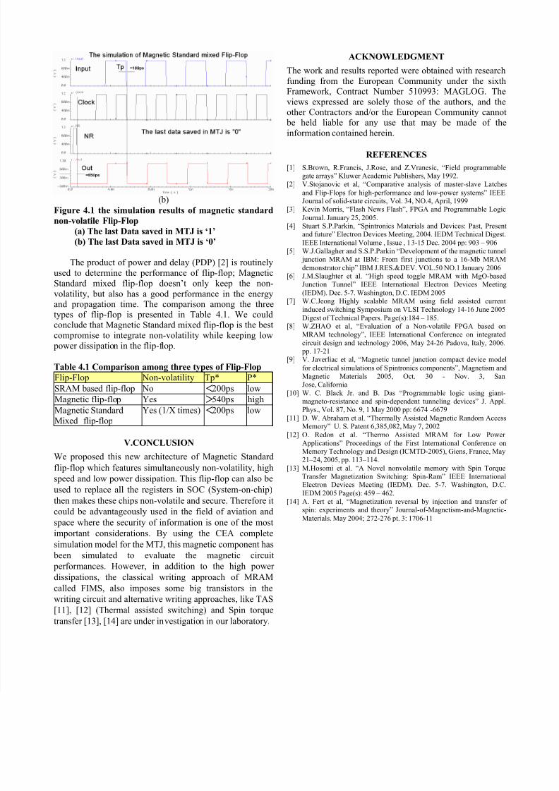
Figure 4.1 the simulation results of magnetic standard
non-volatile Flip-Flop
(a) The last Data saved in MTJ is ‘1’
(b) The last Data saved in MTJ is ‘0’
The product of power and delay (PDP) [2] is routinely
used to determine the performance of flip-flop; MagneticStandard mixed flip-flop doesn’t only keep the non-
volatility, but also has a good performance in the energyand propagation time. The comparison among the threetypes of flip-flop is presented in Table 4.1. We couldconclude that Magnetic Standard mixed flip-flop is the best
compromise to integrate non-volatility while keeping low
power dissipation in the flip-flop.
Table 4.1 Comparison among three types of Flip-Flop
Flip-Flop Non-volatility Tp* P*
SRAM based flip-flop No <200ps low
Magnetic flip-flop Yes >540ps high
Magnetic Standard
Mixed flip-flop
Yes (1/X times) <200ps low
V.CONCLUSION
We proposed this new architecture of Magnetic Standard
flip-flop which features simultaneously non-volatility, high
speed and low power dissipation. This flip-flop can also be
used to replace all the registers in SOC (System-on-chip)
then makes these chips non-volatile and secure. Therefore it
could be advantageously used in the field of aviation and
space where the security of information is one of the most
important considerations. By using the CEA complete
simulation model for the MTJ, this magnetic component has
been simulated to evaluate the magnetic circuit performances. However, in addition to the high power
dissipations, the classical writing approach of MRAM
called FIMS, also imposes some big transistors in the
writing circuit and alternative writing approaches, like TAS
[11], [12] (Thermal assisted switching) and Spin torque
transfer [13], [14] are under investigation in our laboratory.
ACKNOWLEDGMENT
The work and results reported were obtained with research
funding from the European Community under the sixthFramework, Contract Number 510993: MAGLOG. The
views expressed are solely those of the authors, and theother Contractors and/or the European Community cannot
be held liable for any use that may be made of the
information contained herein.
REFERENCES
[1] S.Brown, R.Francis, J.Rose, and Z.Vranesic, “Field programmablegate arrays” Kluwer Academic Publishers, May 1992.
[2] V.Stojanovic et al, “Comparative analysis of master-slave Latches
and Flip-Flops for high-performance and low-power systems” IEEEJournal of solid-state circuits, Vol. 34, NO.4, April, 1999
[3] Kevin Morris, “Flash News Flash”, FPGA and Programmable Logic
Journal. January 25, 2005.[4] Stuart S.P.Parkin, “Spintronics Materials and Devices: Past, Present
and future” Electron Devices Meeting, 2004. IEDM Technical Digest.
IEEE International Volume , Issue , 13-15 Dec. 2004 pp: 903 – 906
[5] W.J.Gallagher and S.S.P.Parkin “Development of the magnetic tunnel junction MRAM at IBM: From first junctions to a 16-Mb MRAM
demonstrator chip” IBM J.RES.&DEV. VOL.50 NO.1 January 2006
[6] J.M.Slaughter et al. “High speed toggle MRAM with MgO-basedJunction Tunnel” IEEE International Electron Devices Meeting
(IEDM). Dec. 5-7. Washington, D.C. IEDM 2005[7] W.C.Jeong Highly scalable MRAM using field assisted current
induced switching Symposium on VLSI Technology 14-16 June 2005
Digest of Technical Papers. Page(s):184 – 185.[8] W.ZHAO et al, “Evaluation of a Non-volatile FPGA based on
MRAM technology”, IEEE International Conference on integrated
circuit design and technology 2006, May 24-26 Padova, Italy, 2006. pp. 17-21
[9] V. Javerliac et al, “Magnetic tunnel junction compact device model
for electrical simulations of Spintronics components”, Magnetism and
Magnetic Materials 2005, Oct. 30 - Nov. 3, SanJose, California
[10] W. C. Black Jr. and B. Das “Programmable logic using giant-magneto-resistance and spin-dependent tunneling devices” J. Appl.Phys., Vol. 87, No. 9, 1 May 2000 pp: 6674 -6679
[11] D. W. Abraham et al. “Thermally Assisted Magnetic Random AccessMemory” U. S. Patent 6,385,082, May 7, 2002
[12] O. Redon et al. “Thermo Assisted MRAM for Low Power
Applications” Proceedings of the First International Conference onMemory Technology and Design (ICMTD-2005), Giens, France, May21–24, 2005, pp. 113–114.
[13] M.Hosomi et al. “A Novel nonvolatile memory with Spin TorqueTransfer Magnetization Switching: Spin-Ram” IEEE InternationalElectron Devices Meeting (IEDM). Dec. 5-7. Washington, D.C.
IEDM 2005 Page(s): 459 – 462.
[14] A. Fert et al, “Magnetization reversal by injection and transfer of spin: experiments and theory” Journal-of-Magnetism-and-Magnetic-
Materials. May 2004; 272-276 pt. 3: 1706-11