Highly efficient semitransparent perovskite solar cells ...
32
This document is downloaded from DR‑NTU (https://dr.ntu.edu.sg) Nanyang Technological University, Singapore. Highly efficient semitransparent perovskite solar cells for four terminal perovskite‑silicon tandems Dewi, Herlina Arianita; Wang, Hao; Li, Jia; Thway, Maung; Sridharan, Ranjani; Stangl, Rolf; Lin, Fen; Aberle, Armin G.; Mathews, Nripan; Bruno, Annalisa; Mhaisalkar, Subodh Gautam 2019 Dewi, H. A., Wang, H., Li, J., Thway, M., Sridharan, R., Stangl, R., . . . Mhaisalkar, S. G. (2019). Highly efficient semitransparent perovskite solar cells for four terminal perovskite‑silicon tandems. ACS Applied Materials & Interfaces, 11(37), 34178‑34187. doi:10.1021/acsami.9b13145 https://hdl.handle.net/10356/142481 https://doi.org/10.1021/acsami.9b13145 This document is the Accepted Manuscript version of a Published Work that appeared in final form in ACS Applied Materials & Interfaces, copyright © American Chemical Society after peer review and technical editing by the publisher. To access the final edited and published work see https://doi.org/10.1021/acsami.9b13145 Downloaded on 23 Mar 2022 20:09:58 SGT
Transcript of Highly efficient semitransparent perovskite solar cells ...
This document is downloaded from DR‑NTU (https://dr.ntu.edu.sg)Nanyang Technological University, Singapore.
Highly efficient semitransparent perovskite solarcells for four terminal perovskite‑silicon tandems
Dewi, Herlina Arianita; Wang, Hao; Li, Jia; Thway, Maung; Sridharan, Ranjani; Stangl, Rolf;Lin, Fen; Aberle, Armin G.; Mathews, Nripan; Bruno, Annalisa; Mhaisalkar, Subodh Gautam
2019
Dewi, H. A., Wang, H., Li, J., Thway, M., Sridharan, R., Stangl, R., . . . Mhaisalkar, S. G. (2019).Highly efficient semitransparent perovskite solar cells for four terminal perovskite‑silicontandems. ACS Applied Materials & Interfaces, 11(37), 34178‑34187.doi:10.1021/acsami.9b13145
https://hdl.handle.net/10356/142481
https://doi.org/10.1021/acsami.9b13145
This document is the Accepted Manuscript version of a Published Work that appeared infinal form in ACS Applied Materials & Interfaces, copyright © American Chemical Societyafter peer review and technical editing by the publisher. To access the final edited andpublished work see https://doi.org/10.1021/acsami.9b13145
Downloaded on 23 Mar 2022 20:09:58 SGT
1
Highly Efficient Semi-Transparent Perovskite Solar
Cells for Four Terminal Perovskite-Silicon Tandems
Herlina Arianita Dewi a#, Hao Wang a#, Jia Li a, Maung Thway b,c, Ranjani Sridharan b, Rolf
Stangl b, Fen Lin b, Armin G. Aberle b,c, Nripan Mathews a,d, Annalisa Bruno a*, Subodh
Mhaisalkar a,d
a. Energy Research Institute @ NTU (ERI@N), Nanyang Technological University, Singapore
637553
b. Solar Energy Research Institute of Singapore (SERIS), National University of Singapore,
Singapore 117574
c. Department of Electrical and Computer Engineering, National University of Singapore,
Singapore 117583
d. School of Materials Science & Engineering, Nanyang Technological University, Singapore
639798
KEYWORDS
perovskite, semi-transparent perovskite solar cell, silicon solar cell, tandem solar cell, efficiency
2
ABSTRACT
Tandem solar cells (SCs) based on perovskite and silicon represent an exciting possibility for a
breakthrough in photovoltaics, enhancing solar cell power conversion efficiency (PCE) beyond
the single junction limit while keeping the production cost low. A critical aspect to push the tandem
PCE close to their theoretical limit is the development of high-performing semi-transparent
perovskite top-cells which also allow suitable near-infrared transmission. Here, we have developed
highly efficient semi-transparent perovskite solar cells (PSCs) based on both mesoporous and
planar architectures, employing Cs0.05(MA0.17FA0.83)0.95Pb(I0.83Br0.17)3 and FA0.87Cs0.13PbI2Br
perovskites with bandgap of 1.58 eV and 1.72 eV respectively which achieved PCEs well above
17% and 14% by detailed control of the deposition methods, thickness and optical transparency of
the interlayers and the semi-transparent electrode. By combining our champion 1.58 eV PSCs
(PCE of 17.7%) with an industrial-relevant low cost n-type Si SCs, a 4 terminals (4T) tandem
efficiency of 25.5% has been achieved. Moreover for the first time, 4T tandem SCs performances
have been measured in the low light intensity regime achieving a PCE of 26.6%, corresponding to
a revealing a relative improvement above 9% compared to standard 1 sun illumination condition.
These results are very promising for their implementations under field-operating conditions.
INTRODUCTION
Silicon solar cells (Si-SCs) dominate the photovoltaic market with their high power conversion
efficiencies (PCE), long term stability, and continuous improvements in the production processes
and costs 1. Heterojunction Si-SCs have recently achieved a record PCE of 26.6% 2-3, close to
their theoretical Auger recombination limit of 29.4% 4. Novel photovoltaic devices are needed to
3
overcome the 30% efficiency ‘barrier’ without significant increase in the cost of production.
Tandem solar cells, which combine multiple cells absorbing complimentary spectral regions, can
exceed 30% efficiencies by minimizing thermalization and absorption losses. Although state-of-
the-art multi-junction solar cells based on III-V semiconductor materials have demonstrated record
efficiencies of 39.2% under 1 sun illumination, their expensive production costs limit the
possibility of their widespread development 5-6.
Instead, tandem SCs based on perovskite and Si-SCs represent a real possibility for breakthrough
photovoltaic performance, enhancing the efficiency of the existing Si-SCs. Indeed, low cost
perovskite solar cells (PSCs) can deliver high PCE 7-8 and good bandgap tenability 9-11, maximizing
bandgap matching with silicon solar cells. Over the last few years, perovskite/Si tandem SCs 12-14
have made impressive progresses reaching record published PCEs of 25.5% 15 (announced of 28%
16) and 27.1% for 2-terminals (2T) and 4-terminals (4T) tandem configurations 17. The primary
difference between these two configurations is that top and bottom cells are series connected in 2T
tandem while they have independent electrical connections in 4T tandem. The main advantage of
a 4T architecture is to allow a broader top cell bandgap selection and independent optimization of
both top and bottom SCs 12, 14, 18.
The development of high performance semi-transparent PSCs is critical to push the tandem
efficiency well above that of a single junction Si-SCs and close to their theoretical efficiency of
43% 12, 19. Highly transparent interfacial layers, i.e. electron transport layer (ETL) and hole
transport layer (HTL) with suitable band alignment, able to guarantee effective charge collection,
are key elements to achieve high-performing PSCs. To date, high-efficiency semi-transparent
PSCs are often realized in n-i-p architecture (glass/Fluorine doped Tin Oxide
(FTO)/ETL/perovskite/HTL/electrode) based on metal-oxide ETLs such as mesoporous TiO2 (m-
4
TiO2) and planar SnO2 (p-SnO2) 20-24. Both these ETLs have significant advantages. The highly
porous thick m-TiO2 scaffold allows reproducible nucleation of the perovskite layer, mitigates
active layer defects, enhance charge collection by decreasing the carrier transport distance, and
prevent electrical shunts 25-27. p-SnO2 has a deep conduction band that facilitate fast electron
extraction and promotes UV-stability 28-30. Moreover, low temperature processed p-SnO2
architecture improves overall SC transparency and is compatible with flexible substrate and 2T
tandem configurations 31-32. HTLs such as 2,2′,7,7′-Tetrakis-(N,N-di-4-methoxyphenylamino)-
9,9′-spirobifluorene (Spiro-OMeTAD) and poly (triarylamine) (PTAA) are extensively used as
hole transporting materials with efficient hole transport and electron-blocking properties 8, 33-35,
resulting in the highest efficiencies. Another challenge to achieve high-PCE is the transmission at
wavelengths longer than the perovskite bandgap that determines current generation in the bottom
Si-SCs. Top PSCs in 4T tandem have to utilize two layers of transparent electrodes, which are the
main cause for parasitic absorption losses. Perovskites with ~1.55 eV bandgap only allow NIR
light to reach the bottom Si-SCs, whereas PSCs with higher bandgap (>1.55 eV) result in a wider
transparency window but yield lower efficiencies. Thus, a balance between overall transparency
and efficiency is a critical consideration. Recent results clearly indicate that for 4T tandem
perovskite-silicon cells, top cells make a major contribution towards higher efficiencies (Table
S114, 17, 21, 24, 36-48).
In this work, we have developed highly efficient, semi-transparent PSCs using two different
bandgaps and different architectures to investigate the best performing top cell for a 4T tandem
configuration. Cs0.05(MA0.17FA0.83)0.95Pb(I0.83Br0.17)3 and FA0.87Cs0.13PbI2Br perovskites with
bandgap of 1.58 eV and 1.72 eV respectively, were implemented in both m-TiO2 and p-SnO2
architectures. The semi-transparent PSCs demonstrate efficiencies above 17% and above 14% for
5
1.58 eV and 1.72 eV band-gap devices in both m-TiO2 and p-SnO2. Combining 1.58 eV and 1.72
eV semi-transparent PSCs with bottom Si-SCs, the 4T tandem SCs achieved PCEs as high as
25.5% and 22.7% respectively. Silicon and perovskite single junctions and 4T tandem SCs have
been also investigated in intensity regime between 1 and 0.1 sun in order to emulate realistic
operating conditions. 4T tandem PCEs showed a relative 9.7% PCE improvement at the lowest
illumination respect to the standard (1 sun) conditions.
RESULTS AND DISCUSSION
Perovskite Thin Film Characterization
Varying the perovskite bandgap in PSCs is a straightforward approach to examine the effect of
top cell transparency on the 4T tandem PCE. Indeed, aiming at unveil the trade-off between
transparency spectral range and efficiency in pursuit of best performing 4T tandem SCs,
perovskites with different bangdap have been implemented. Perovskites with mixed cations and
halide compositions have been synthetized - Cs0.05(MA0.17FA0.83)0.95Pb(I0.83Br0.17)349 and
FA0.87Cs0.13PbI2Br - to attain bandgaps of 1.58 eV and 1.72 eV respectively (Figure 1a). These
compositions have been chosen for suitable bandgap match with Si-SC, stability, and fabrication
reproducibility 14, 19, 49. The valence band (VB) levels for these perovskites have been measured
using photoelectron spectroscopy in air (PESA), whereas the conduction band (CB) levels were
derived by combing them with their optical bandgaps Figure S1a. The corresponding energy levels
are shown in Figure S1b. The CB values of 1.58 eV perovskite and 1.72 eV perovskite are
estimated to be at -4.22 eV and -4.15 eV, which show a favourable energy level alignment with
both m-TiO2 and p-SnO2 layers, suggesting a good and efficient charge injection to the electron
transport layers.
6
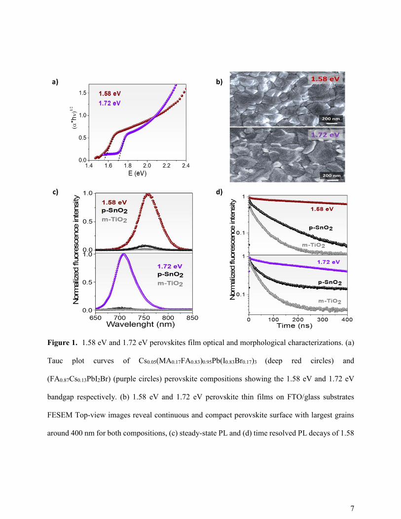
Both 1.58 eV and 1.72 eV perovskites thin films display continuous and compact morphologies
as indicated in the Field Emission Scanning Electron Microscopy (FESEM) images (Figure 1b).
Specifically, the 1.58 eV perovskite film shows a homogenous distribution of large grains while
in the 1.72 eV a larger spread of grain sizes can be observed. The crystal structures of both 1.58
eV and 1.72 eV perovskites have been further characterized by X-Ray diffraction (XRD) (Figure
S2). Both perovskite compositions show a PbI2 excess at 12.4° which is beneficial to both passivate
the perovskite surface and to increase the charge mobility and consequently the device
performance 50-52.
Carrier lifetime and injection properties of 1.58 eV and 1.72 eV perovskite thin films with and
without the electron quenching layer have been studied by steady state and time resolved photo-
luminescence (PL) measurements. The steady state PL spectra peak at 760 nm and 710 nm for the
1.58 eV and 1.72 eV perovskites respectively and they both composition show a significant
quenching (above 90%) when the thin film is deposited on top of the m-TiO2 and p-SnO2 layers
confirming the efficient charge injection (Figure 1c and Table S2) from the perovskite to the ETL.
Time resolved PL (TRPL) measurements of the (Figure 1d). Pristine 1.58 eV and 1.72 eV
perovskites reveal long fluorescence lifetimes of 488 ns and 292 ns respectively, which confirms
their good optoelectronic properties and low defect densities. Moreover, both ETLs effectively
quench the fluorescence emission, reducing the 1.58 eV perovskite excitons lifetimes to 28 ns and
41 ns for m-TiO2 and p-SnO2 respectively. Using a similar structure, 1.72 eV perovskite lifetime
has been reduced to 23 ns and 60 ns on m-TiO2 and p-SnO2 respectively. The substantial PL
quenching is an evidence of efficient charge separation necessary for good performance in SCs.
Slightly higher quenching for m-TiO2 is hypothesized to be due to the larger surface area contact
with perovskite films as compared to p-SnO2.
7
Figure 1. 1.58 eV and 1.72 eV perovskites film optical and morphological characterizations. (a)
Tauc plot curves of Cs0.05(MA0.17FA0.83)0.95Pb(I0.83Br0.17)3 (deep red circles) and
(FA0.87Cs0.13PbI2Br) (purple circles) perovskite compositions showing the 1.58 eV and 1.72 eV
bandgap respectively. (b) 1.58 eV and 1.72 eV perovskite thin films on FTO/glass substrates
FESEM Top-view images reveal continuous and compact perovskite surface with largest grains
around 400 nm for both compositions, (c) steady-state PL and (d) time resolved PL decays of 1.58
8
eV and 1.72 eV perovskite thin films on glass and on top of m-TiO2 and p-SnO2 layers, obtained
with excitation wavelength of 405 nm, <2 J/cm2, 40 MHz.
Semi-Transparent Perovskite Solar Cells
The selection of top, bottom electrode contacts and charge extraction materials is critical to
minimizing the overall optical losses, maximizing light transmission to the bottom Si-SC and
enabling high performance 4T tandem 57, 58. The PSCs structures employed in this work are shown
on Figure 2a. PSCs were implemented on top of high quality glass/FTO substrates with good
conductivity (sheet resistance of 15 Ω/cm) and high transparency over visible and infrared spectra
(Figure S3a), guaranteeing a good quality bottom electrode. Indeed, other FTO substrates with
lower sheet resistance (7 Ω /cm) have a much lower transparency in the infrared range, which
could significantly hamper the overall 4T performance (Figure S3b). As ETLs, wide bandgap
semiconductors (TiO2 and SnO2) can provide high transparency 59, 60 and good mobility 30, 61. Both
these properties allowed us to implement efficient cells in both mesoporous and planar
architectures.
The perovskite deposition process has been optimized for both band gaps to obtain large grains
and continuous films (Figure 1b, and details in the Experimental section). Tuning of perovskite
thickness is also necessary to resolve the trade-off between the transparency and efficiency of the
perovskite absorber 62. Different precursors’ concentrations have also been screened to tune the
film thickness for achieving the highest efficiency (Figure S4). The precursors’ concentration of
1.5 M leads to a film thickness of ~500 nm and to the best performing cells. We kept thicknesses
constant for both mesoporous and planar architectures (Figure 2b). Spiro-OMeTAD was chosen
as the HTM due to its good band alignment (Figure S1b) and efficient charge transport. Although
9
Spiro-OMeTAD present a non-negligible parasitic absorption in the UV region (300-400 nm) 45,
63, it does not affect the overall 4T tandem performance since the top cells are illuminated through
the glass/FTO side and the UV light component is absorbed by the perovskite layer before reaching
the Spiro-OMeTAD layer.
Semi-transparent PSCs employed sputtered indium tin oxide (ITO) as top transparent conducing
electrode. The ITO thickness has been carefully optimized, through varying the ITO sputtering
power (Figure S5). The highest transparency corresponds to the lowest power of 25 W and to ITO
film thickness of around 220 nm. Thinner film could improve the transparency but at the cost of
higher sheet resistance. For each sputtering conditions, semi-transparent PSCs have been
fabricated and their photovoltaic performances are reported in Table S3. Details on deposition
conditions are reported in Methods section. In addition of reduced total transparency of the semi-
transparent PSCs, the high power sputtering condition (30 W) also induces damage on under-layer
as shown by the lower device performances. Although our deposition process has been optimized
to maximize the transparency at reduced sputtering power, the best operating PSCs still required a
thin thermally evaporated Ag film as buffer layer to protect the under-layer and guarantee good
ITO crystallinity, and minimally reduces the total transmission. The effect of Ag thickness on the
total cell transparency has been also studied previously 63. The optical transmittance of individual
layers and top electrode of the semi-transparent PSCs, with 1.58 eV perovskite as absorber
material, are shown in Figure S6. Although the transparency for each layer has been carefully
optimized, the total device transparency could be further improved by minimizing reflectance
between device sub-layers.
10
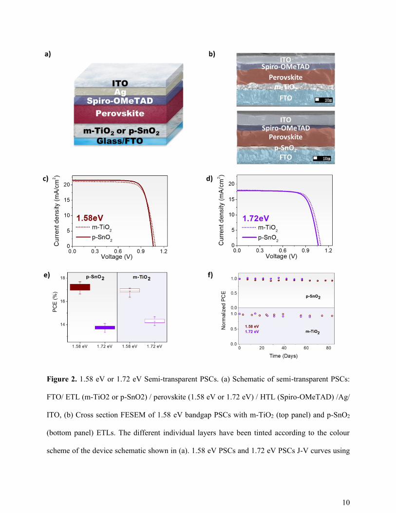
Figure 2. 1.58 eV or 1.72 eV Semi-transparent PSCs. (a) Schematic of semi-transparent PSCs:
FTO/ ETL (m-TiO2 or p-SnO2) / perovskite (1.58 eV or 1.72 eV) / HTL (Spiro-OMeTAD) /Ag/
ITO, (b) Cross section FESEM of 1.58 eV bandgap PSCs with m-TiO2 (top panel) and p-SnO2
(bottom panel) ETLs. The different individual layers have been tinted according to the colour
scheme of the device schematic shown in (a). 1.58 eV PSCs and 1.72 eV PSCs J-V curves using
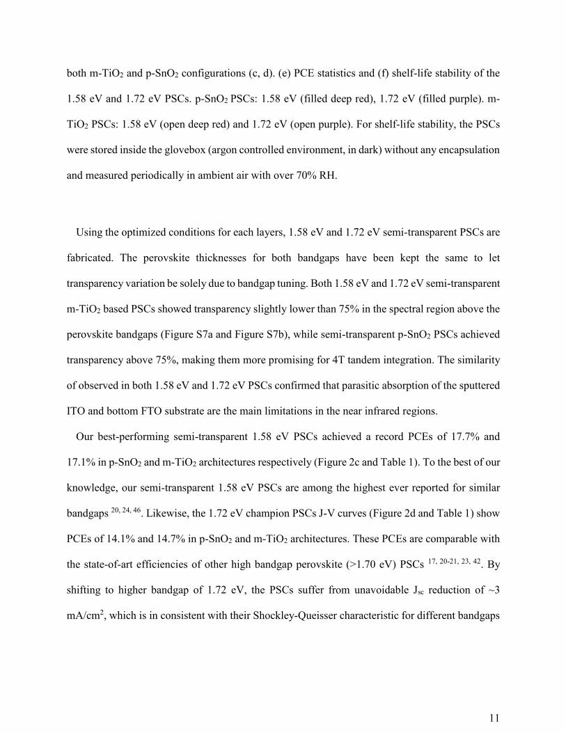
11
both m-TiO2 and p-SnO2 configurations (c, d). (e) PCE statistics and (f) shelf-life stability of the
1.58 eV and 1.72 eV PSCs. p-SnO2 PSCs: 1.58 eV (filled deep red), 1.72 eV (filled purple). m-
TiO2 PSCs: 1.58 eV (open deep red) and 1.72 eV (open purple). For shelf-life stability, the PSCs
were stored inside the glovebox (argon controlled environment, in dark) without any encapsulation
and measured periodically in ambient air with over 70% RH.
Using the optimized conditions for each layers, 1.58 eV and 1.72 eV semi-transparent PSCs are
fabricated. The perovskite thicknesses for both bandgaps have been kept the same to let
transparency variation be solely due to bandgap tuning. Both 1.58 eV and 1.72 eV semi-transparent
m-TiO2 based PSCs showed transparency slightly lower than 75% in the spectral region above the
perovskite bandgaps (Figure S7a and Figure S7b), while semi-transparent p-SnO2 PSCs achieved
transparency above 75%, making them more promising for 4T tandem integration. The similarity
of observed in both 1.58 eV and 1.72 eV PSCs confirmed that parasitic absorption of the sputtered
ITO and bottom FTO substrate are the main limitations in the near infrared regions.
Our best-performing semi-transparent 1.58 eV PSCs achieved a record PCEs of 17.7% and
17.1% in p-SnO2 and m-TiO2 architectures respectively (Figure 2c and Table 1). To the best of our
knowledge, our semi-transparent 1.58 eV PSCs are among the highest ever reported for similar
bandgaps 20, 24, 46. Likewise, the 1.72 eV champion PSCs J-V curves (Figure 2d and Table 1) show
PCEs of 14.1% and 14.7% in p-SnO2 and m-TiO2 architectures. These PCEs are comparable with
the state-of-art efficiencies of other high bandgap perovskite (>1.70 eV) PSCs 17, 20-21, 23, 42. By
shifting to higher bandgap of 1.72 eV, the PSCs suffer from unavoidable Jsc reduction of ~3
mA/cm2, which is in consistent with their Shockley-Queisser characteristic for different bandgaps
12
53-54, whereas, loss in both Voc and FF, may indicate presence of more carrier recombination and
non-uniformity in the absorber grain sizes distribution.
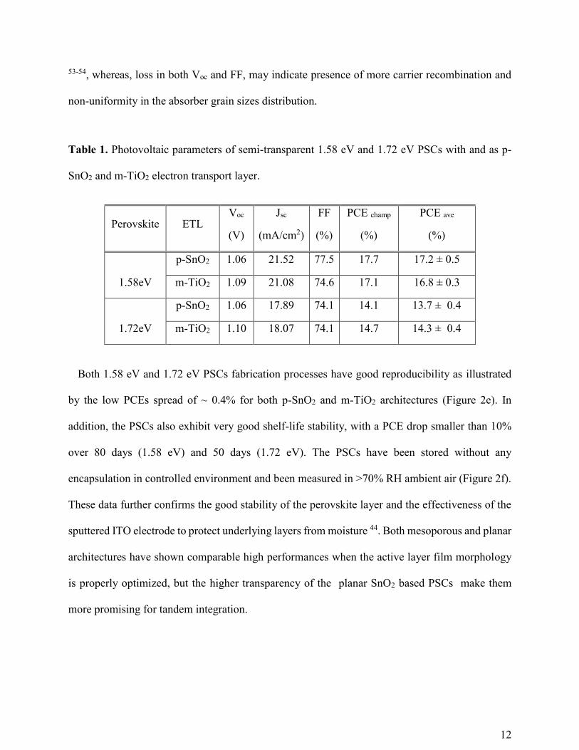
Table 1. Photovoltaic parameters of semi-transparent 1.58 eV and 1.72 eV PSCs with and as p-
SnO2 and m-TiO2 electron transport layer.
Perovskite ETL Voc
(V)
Jsc
(mA/cm2)
FF
(%)
PCE champ
(%)
PCE ave
(%)
1.58eV
p-SnO2 1.06 21.52 77.5 17.7 17.2 ± 0.5
m-TiO2 1.09 21.08 74.6 17.1 16.8 ± 0.3
1.72eV
p-SnO2 1.06 17.89 74.1 14.1 13.7 ± 0.4
m-TiO2 1.10 18.07 74.1 14.7 14.3 ± 0.4
Both 1.58 eV and 1.72 eV PSCs fabrication processes have good reproducibility as illustrated
by the low PCEs spread of ~ 0.4% for both p-SnO2 and m-TiO2 architectures (Figure 2e). In
addition, the PSCs also exhibit very good shelf-life stability, with a PCE drop smaller than 10%
over 80 days (1.58 eV) and 50 days (1.72 eV). The PSCs have been stored without any
encapsulation in controlled environment and been measured in >70% RH ambient air (Figure 2f).
These data further confirms the good stability of the perovskite layer and the effectiveness of the
sputtered ITO electrode to protect underlying layers from moisture 44. Both mesoporous and planar
architectures have shown comparable high performances when the active layer film morphology
is properly optimized, but the higher transparency of the planar SnO2 based PSCs make them
more promising for tandem integration.
13
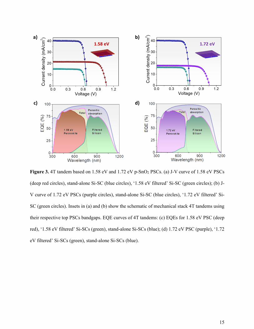
4T Perovskite-Silicon Tandem
Both 1.58 eV and 1.72 eV semi-transparent PSCs with p-SnO2 ETL have been implemented in
a 4T tandem configuration with small-size (1cm2) n-type monoPolyTM bottom Si-SCs (insets of
Figure 3a and Figure 3b) 55. The 1cm2 localized grown Si-SCs has been specifically designed to
eliminate the effect of edge recombination losses as compared to conventional laser cutting process
from full size silicon wafer. The schematic of silicon bottom cell is shown in Figure S8. Fabrication
and characterization details of the bottom Si-SCs are reported in the experimental section and will
be further described in a future work. As shown in Table 2, the stand-alone Si-SC has a PCE of
21.1% under the standard AM1.5G spectrum. As the Si-SCs under tandem configurations only
receive the light filtered by the top PSCs, they effectively perform under a much lower injection
level compared to standard AM1.5G conditions, resulting in much lower Voc and Jsc values. The
effective add-on efficiency from the Si-SC under the 1.58 eV PSCs is 7.8% (Figure 3a). A 4T
tandem efficiency of 25.5% was achieved by combining the 1.58 eV PSC with the Si-SC.
Instead, when in the 4T tandem configuration the incident light is filtered by the 1.72 eV PSCs,
a larger fraction light can reach the bottom Si SCs and concomitantly its PCE contribution rises to
8.3%. This higher value is mostly driven by the lower Jsc reduction (25 mA/cm2 instead 23.8
mA/cm2) (Figure 3b). Although Si-SCs contribute a higher effective add-on efficiency, the 1.72
eV PSCs PCE is still much lower than the 1.58 eV PSCs and the total 4T tandem efficiency
achieved in this configuration was only f 22.4%. Interestingly, the Jsc values for the 1.72 eV PSCs
and the Si-CSs filtered by 1.72 eV PSCs are comparable, indicating the potential of this perovskite
composition for future 2T monolithic integration where current matching between the top and
bottom cells is required. The EQE of both 1.58 eV and 1.72 eV semi-transparent PSCs show a
very sharp edge at their particular bandgap indicating the good absorption of the thick perovskite
14
layers (Figure 3c and Figure 3d). The Si-SCs EQEs reach around 75% under the perovskite filter
in the infrared range closely matching the transparency value of the top PSCs. Although 4T tandem
efficiency is higher than each of the stand-alone sub-cells, the EQEs clearly show presence of
parasitic absorption of the top PSCs which limits the efficiency of the filtered Si-SC. The 4T
tandem SCs performances of m-TiO2 1.58 eV and 1.72 eV PSCs show a similar trend to the p-
SnO2 PSC. Indeed, 4T tandem PCEs reached of 24.6% and 22.7% for 1.58 eV and 1.72 eV PSCs
respectively (Figure S9a and Figure S9b). The photovoltaic parameters are summarized in Table
S4. These less transparent top PSCs, as compared to the p-SnO2 counterpart, resulted in lower Jsc
in the filtered Si-SCs as clearly shown in the Si-SCs EQE (Figure S9c and Figure S9d).
For both mesoporous and planar architectures, the absolute PCE gains from stand-alone Si-SCs
to a 4T perovskite-on-Si tandem are ~5% and ~2% with 1.58eV and 1.72eV top PSCs, respectively,
highlighting the advantage of deploying a multi-junction configuration to better utilize the solar
irradiance spectrum.
15
Figure 3. 4T tandem based on 1.58 eV and 1.72 eV p-SnO2 PSCs. (a) J-V curve of 1.58 eV PSCs
(deep red circles), stand-alone Si-SC (blue circles), ‘1.58 eV filtered’ Si-SC (green circles); (b) J-
V curve of 1.72 eV PSCs (purple circles), stand-alone Si-SC (blue circles), ‘1.72 eV filtered’ Si-
SC (green circles). Insets in (a) and (b) show the schematic of mechanical stack 4T tandems using
their respective top PSCs bandgaps. EQE curves of 4T tandems: (c) EQEs for 1.58 eV PSC (deep
red), ‘1.58 eV filtered’ Si-SCs (green), stand-alone Si-SCs (blue); (d) 1.72 eV PSC (purple), ‘1.72
eV filtered’ Si-SCs (green), stand-alone Si-SCs (blue).
16
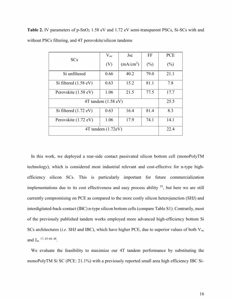
Table 2. IV parameters of p-SnO2 1.58 eV and 1.72 eV semi-transparent PSCs, Si-SCs with and
without PSCs filtering, and 4T perovskite/silicon tandems
SCs Voc
(V)
Jsc
(mA/cm2)
FF
(%)
PCE
(%)
Si unfiltered 0.66 40.2 79.0 21.1
Si filtered (1.58 eV) 0.63 15.2 81.1 7.8
Perovskite (1.58 eV) 1.06 21.5 77.5 17.7
4T tandem (1.58 eV) 25.5
Si filtered (1.72 eV) 0.63 16.4 81.4 8.3
Perovskite (1.72 eV) 1.06 17.9 74.1 14.1
4T tandem (1.72eV) 22.4
In this work, we deployed a rear-side contact passivated silicon bottom cell (monoPolyTM
technology), which is considered most industrial relevant and cost-effective for n-type high-
efficiency silicon SCs. This is particularly important for future commercialization
implementations due to its cost effectiveness and easy process ability 55, but here we are still
currently compromising on PCE as compared to the more costly silicon heterojunction (SHJ) and
interdigitated-back-contact (IBC) n-type silicon bottom cells (compare Table S1). Contrarily, most
of the previously published tandem works employed more advanced high-efficiency bottom Si
SCs architectures (i.e. SHJ and IBC), which have higher PCE, due to superior values of both Voc
and Jsc 17, 43-44, 48.
We evaluate the feasibility to maximize our 4T tandem performance by substituting the
monoPolyTM Si SC (PCE: 21.1%) with a previously reported small area high efficiency IBC Si-
17
SC (PCE: 24.4% 56) in conjunction with our 17.7% p-SnO2 1.58 eV ST-PSC. Assuming the same
relative drop in efficiency for the 24.4% IBC Si SCs as the one observed for the monoPolyTM
SCs, a PCE of 9.1% would be achieved, when filtered with our 1.58 eV ST-PSC. This value is
significantly higher to the 7.8% PCE measured for monoPolyTM Si SC. The 4T tandem
configuration deploying a 1.58 eV ST-PSCs as top cell and an IBC Si SC as bottom cells could
then lead to a PCE of 26.8%.
Moreover light management strategies could also be implemented to further improve our 4T
tandem cell efficiency. These are likely to arise from enhancement in top perovskite cell
transparency by minimizing overall reflectance losses through proper coatings and reduction of
parasitic absorption 46, 56-57.
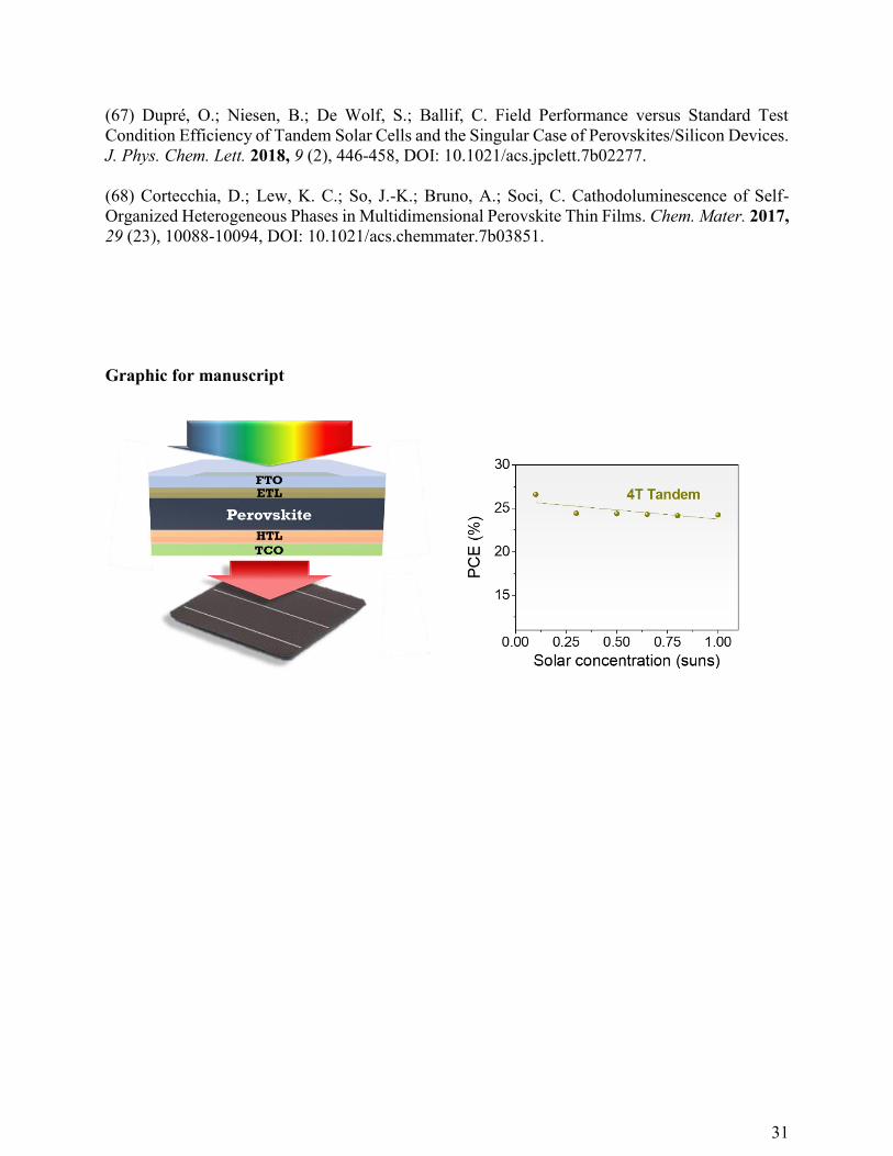
4T Perovskite-Silicon Tandem under Low Light Intensity
We also explore the feasibility of 4T tandem SCs for realistic operation, when both spectral
distribution and intensity of the sunlight radiance reaching the SCs can vary during the daytime
and the season. Therefore, understanding the PCE trend under different light conditions is critical
for field-operating conditions. Here, we investigate both perovskite and silicon single junction SCs
and 4T tandem SC photovoltaic parameters under different light intensities ranging from 0.1 to 1
Sun. The 4T tandem PCEs are reported in Figure 4a and b, while the detailed Jsc, Voc, and FF are
shown in Figure S10a, Figure S10b, and Figure S10c. Even if theoretical studies have shown the
simulated trend of both 2T and 4T tandem SCs under different illuminations 58-59, to the best our
knowledge these are the first experimental data showing the trend of a perovskite-silicon tandem
solar cells under low intensity illumination.
18
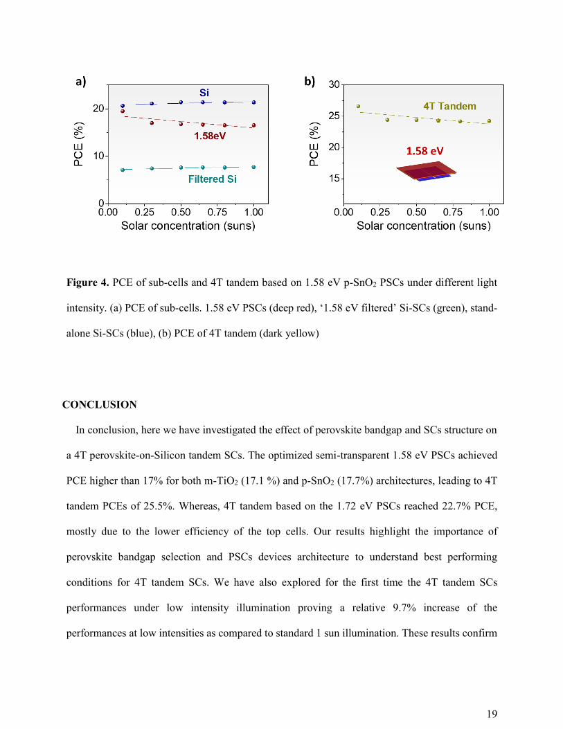
Silicon SCs, either under direct illumination (stand-alone) or filtered by the perovskite, exhibit
very marginal PCE reduction as the illumination intensity decreases, with the highest relative drop
around 5% at 0.1 sun (Figure 4a). The detailed photovoltaic characteristics for stand-alone and
filtered Si SC, Figure S10, are consistent with previous works 60. On the other hand, the PCE of
1.58 eV semi-transparent perovskite SCs remains almost constant in the light intensity region
between 1-0.5 sun, while it slightly increases at even lower intensities (0.5-0.1 sun) reaching the
maximum value of 19.5% at 0.1 sun (18% relative improvement) (Figure 4a). The perovskite SC
Jsc and FF mainly drive the PCE increase. The Jsc linear trend with light intensity of single junction
perovskite SC has been also previously reported, indicating good charge separation at the
perovskite and transport layers interface regardless of different light intensity 61-63 (Figure S10a).
The increase of FF with the intensity decrease suggests a reduced charge recombination under
lower light intensity (Figure S10b). At the same time Voc only slightly decreases from 1 to 0.1 sun
in agreement with the hypothesis of a reduced number of electron generated (Figure S10c) 64-65.
As a combined effect of the behaviour of both sub-cells, the 4T tandem SCs exhibits a stable
PCE also under lower intensities reaching 26.6% of PCE and a 9.7% relative improvement of the
PCE when operated at 0.1 sun (Figure 4b), suggesting that 4T tandem configuration is versatile to
be implemented in different illumination conditions. Our experimental 4T results under different
light intensity are also in line with theoretical simulations which have shown that 4T tandem SCs
under practical condition can achieve higher PCE, which does not critically depends on solar
radiance intensity, as compared to 2T counterpart 66-67. Although our studies also justify good
performance of single junction perovskites and silicon SCs under low light intensity regime, the
presented 4T tandem is able to outperform the single junction due to better spectrum light utilized
and less thermalisation losses.
19
Figure 4. PCE of sub-cells and 4T tandem based on 1.58 eV p-SnO2 PSCs under different light
intensity. (a) PCE of sub-cells. 1.58 eV PSCs (deep red), ‘1.58 eV filtered’ Si-SCs (green), stand-
alone Si-SCs (blue), (b) PCE of 4T tandem (dark yellow)
CONCLUSION
In conclusion, here we have investigated the effect of perovskite bandgap and SCs structure on
a 4T perovskite-on-Silicon tandem SCs. The optimized semi-transparent 1.58 eV PSCs achieved
PCE higher than 17% for both m-TiO2 (17.1 %) and p-SnO2 (17.7%) architectures, leading to 4T
tandem PCEs of 25.5%. Whereas, 4T tandem based on the 1.72 eV PSCs reached 22.7% PCE,
mostly due to the lower efficiency of the top cells. Our results highlight the importance of
perovskite bandgap selection and PSCs devices architecture to understand best performing
conditions for 4T tandem SCs. We have also explored for the first time the 4T tandem SCs
performances under low intensity illumination proving a relative 9.7% increase of the
performances at low intensities as compared to standard 1 sun illumination. These results confirm
20
the potential of the 4T tandem SCs in field-operating conditions, as predicted from previous
theoretical simulations.
EXPERIMENTAL SECTION
Perovskite deposition
The 1.58 eV perovskite (Cs0.05(MA0.17FA0.83)0.95Pb(I0.83Br0.17)3) precursor solution, was prepared
following ref. 49 and was spin-coated at 1000 rpm for 10 s followed by 6000 rpm for 17 s. The 1.72
eV perovskite (FA0.83Cs0.17PbI2Br) was spin-coated at 2000 rpm for 10 s followed by 6000 rpm
for 30 s. Both perovskites utilized chlorobenzene as secondary solvent and undergo 100 °C for 1
h post-annealing inside argon-filled glovebox.
Perovskite film characterization
Photo Electron Spectroscopy in Air (PESA) measurements was recorded with a Riken Keiki
AC-2 PESA spectrometer with a power setting of 800 nW and a power number of 0.5. Absorbance
(A) and Transmission (T) spectra were recorded using UV-Vis-NIR Spectrophotometer (UV3600,
Shimadzu) equipped with an integrating sphere (300-1200 nm wavelength). Morphological
characterization for both top view perovskite film and cross section of the complete devices were
recorded using a Field Emission Scanning Electron Microscope (FESEM, JEOL JSM-7600F, 5
kV and 10 mA). X-Ray Diffraction (XRD) patterns were recorded on (Bruker D8 Advance).
Steady state photoluminescence spectra had been measured using a top-table Fluoromax-5 system.
TRPL decays were collected using a micro-PL setup and a Picoquant PicoHarp 300 time-correlated
single photon counting (TCSPC) system and a laser diode (Picoquant P-C-405B, λ = 405 nm, <2
J/cm2, 40 MHz) as excitation source 68.
21
Semi-transparent perovskite top cell
Substrate preparation: Fluorine doped tin oxide (FTO) glass substrates (TEC-15) were cleaned
in decon soap and treated under UV ozone for 15 min prior to usage. ETLs: High temperature m-
TiO2 was fabricated following the procedure in ref 16. Low temperature p-SnO2: 0.1 M SnCl2.2H2O
(Sigma Aldrich) with 8% InCl3 (Sigma Aldrich) doped was dissolved in ethanol and stirred for 12
hours. The dissolved SnCl2 solution was spun coated using a two-step program at 1500 rpm for 10
s followed by 5000 rpm for 10 s. The substrate then was preheated at 80°C for 10 min and
subsequently heated to 180°C for 1h in air to completely oxidize the SnCl2 to SnO2. HTL: Spiro-
OMeTAD (70 mg/mL in chlorobenzene) with addition of 4-tert-butylpyridine, lithium
bis(trifluoromethylsulphonyl)imide (520 mg/mL in acetonitrile (ACN)) and FK209
(37.6mg/100 L of ACN) was spin-coated at 5000 rpm for 30 s inside glovebox. Back contact:
Indium tin oxide (ITO) was deposited using DC sputter at 25 W for 1.5 hour to form transparent
top electrode. Prior ITO deposition, a 1 nm thin Ag was thermally evaporated as buffer layer.
Silicon bottom cell
The Si bottom cells were fabricated on 6-inch n-type pseudo-square silicon wafers (180 µm, 2
ohm-cm) using industrially relevant tools. The fabrication procedure followed the standard
fabrication steps of monoPoly cells 55. The polycrystalline silicon layer used in this work was
deposited using low pressure chemical vapour deposition (LPCVD) instead of plasma enhanced
chemical vapour deposition (PEVCD) method. Furthermore, a localized small-area diffused front
emitter was realized to limit the active cell area to 1 cm2. The finished cells were passivated by
AlOx/SiNx stack on the front and SiNx on the rear using PECVD, with screen-printed H-pattern
22
metal grids on both sides. The H-pattern grids were custom-designed within the active area to
minimize the dark current loss through non-illuminated areas.
Characterizations
The J-V measurements were measured using (Wavelabs Sinus-220 LEDs IV tester). The external
quantum efficiency (EQE) of both perovskite and silicon solar cells were determined using a small
beam spectral response measurement system (Bentham PVE300) in DC mode using dual
xenon/quartz halogen light source without light bias. An aperture mask with dimension of 0.3 cm
x 0.3 cm was used for perovskite J-V measurement, while the silicon bottom cell area is 1 cm2.
The Si-SCs measured efficiency is taking care of the shading loss.
ASSOCIATED CONTENT
Supporting Information
The Supporting Information is available free of charge on the ACS Publications website. Figure
S1: PESA and band diagram. Figure S2: XRD pattern. Figure S3: Glass/FTO transparency. Figure
S4: Perovskite concentration variation. Figure S5: Transparency curves with various ITO sputter
power. Figure S6: Transparency curves of individual layers. Figure S7: Semi-transparent
perovskite transparency curves. Figure S8: silicon cell schematic. Figure S9: 4T tandem J-V curves
and EQE. Figure S10: Photovoltaic under different illumination intensity. Table S1: Summary of
4T tandem efficiencies. Table S2: Photoluminescence quenching efficiency. Table S3: J-V curves
different sputter power. Table S4: m-TiO2 device photovoltaic summary
23
AUTHOR INFORMATION
Corresponding Author
Email: [email protected]
ORCID
Maung Thway: 0000-0003-4904-0639
Armin G. Aberle: 0000-0003-0456-2070
Nripan Mathews: 0000-0001-5234-0822
Annalisa Bruno: 0000-0002-6963-1682
Subodh Mhaisalkar: 0000-0002-9895-2426
Author Contributions
# These authors contributed equally.
HAD, HW, JL, NM, AB and SM developed and characterized the semitransparent perovskite solar
cells. MT, RS, RS FL, and AA developed and characterized the Silicon solar cells. The manuscript
was drafted by HAD and AB and finalized with contributions of all the authors. This work was
coordinated by AB and SM. All the authors have given approval to the final version of the
manuscript.
Notes
The authors declare no competing financial interest.
24
ACKNOWLEDGMENT
This research is supported by the National Research Foundation, Prime Minister’s Office,
Singapore under Energy Innovation Research Program (Grant number, NRF2015EWT-
EIRP003-004 and NRF-CRP14-2014-03 and Solar CRP: S18-1176-SCRP)
REFERENCES
(1) Jordan, D. C.; Kurtz, S. R.; VanSant, K.; Newmiller, J. Compendium of Photovoltaic
Degradation Rates. Prog. Photovoltaics: Research and Applications 2016, 24 (7), 978-989, DOI:
doi:10.1002/pip.2744.
(2) Yoshikawa, K.; Yoshida, W.; Irie, T.; Kawasaki, H.; Konishi, K.; Ishibashi, H.; Asatani, T.;
Adachi, D.; Kanematsu, M.; Uzu, H.; Yamamoto, K. Exceeding Conversion Efficiency of 26% by
Heterojunction Interdigitated Back Contact Solar Cell with Thin Film Si Technology. Sol. Energy
Mater. Sol. Cells 2017, 173, 37-42, DOI: https://doi.org/10.1016/j.solmat.2017.06.024.
(3) Yoshikawa, K.; Kawasaki, H.; Yoshida, W.; Irie, T.; Konishi, K.; Nakano, K.; Uto, T.; Adachi,
D.; Kanematsu, M.; Uzu, H.; Yamamoto, K. Silicon Heterojunction Solar Cell with Interdigitated
Back Contacts for a Photoconversion Efficiency Over 26%. Nat. Energy 2017, 2, 17032, DOI:
10.1038/nenergy.2017.32.
(4) Richter, A.; Hermle, M.; Glunz, S. W. Reassessment of the Limiting Efficiency for Crystalline
Silicon Solar Cells. IEEE J. Photovolt. 2013, 3 (4), 1184-1191, DOI:
10.1109/JPHOTOV.2013.2270351.
(5) Essig, S.; Allebé, C.; Remo, T.; Geisz, J. F.; Steiner, M. A.; Horowitz, K.; Barraud, L.; Ward,
J. S.; Schnabel, M.; Descoeudres, A.; Young, David L.; Woodhouse, M.; Despeisse, M.; Ballif,
C.; Tamboli, A. Raising the One-sun Conversion Efficiency of III–V/Si Solar Cells to 32.8% for
Two Junctions and 35.9% for Three Junctions. Nat. Energy 2017, 2, 17144, DOI:
10.1038/nenergy.2017.144
(6) Green, M. A.; Hishikawa, Y.; Warta, W.; Dunlop, E. D.; Levi, D. H.; Hohl-Ebinger, J.; Ho-
Baillie, A. W. H. Solar Cell Efficiency Tables (version 50). Prog. Photovoltaics: Research and
Applications 2017, 25 (7), 668-676, DOI: doi:10.1002/pip.2909.
(7) Correa-Baena, J.-P.; Abate, A.; Saliba, M.; Tress, W.; Jesper Jacobsson, T.; Grätzel, M.;
Hagfeldt, A. The Rapid Evolution of Highly Efficient Perovskite Solar Cells. Energy Environ. Sci.
2017, 10 (3), 710-727, DOI: 10.1039/c6ee03397k.
(8) Yang, W. S.; Park, B.-W.; Jung, E. H.; Jeon, N. J.; Kim, Y. C.; Lee, D. U.; Shin, S. S.; Seo, J.;
Kim, E. K.; Noh, J. H.; Seok, S. I. Iodide Management in Formamidinium-lead-halide–based
25
Perovskite Layers for Efficient Solar Cells. Science 2017, 356 (6345), 1376-1379, DOI:
10.1126/science.aan2301.
(9) Noh, J. H.; Im, S. H.; Heo, J. H.; Mandal, T. N.; Seok, S. I. Chemical Management for Colorful,
Efficient, and Stable Inorganic–Organic Hybrid Nanostructured Solar Cells. Nano Lett. 2013, 13
(4), 1764-1769, DOI: 10.1021/nl400349b.
(10) Eperon, G. E.; Leijtens, T.; Bush, K. A.; Prasanna, R.; Green, T.; Wang, J. T.-W.; McMeekin,
D. P.; Volonakis, G.; Milot, R. L.; May, R.; Palmstrom, A.; Slotcavage, D. J.; Belisle, R. A.; Patel,
J. B.; Parrott, E. S.; Sutton, R. J.; Ma, W.; Moghadam, F.; Conings, B.; Babayigit, A.; Boyen, H.-
G.; Bent, S.; Giustino, F.; Herz, L. M.; Johnston, M. B.; McGehee, M. D.; Snaith, H. J. Perovskite-
perovskite Tandem Photovoltaics with Optimized Band Gaps. Science 2016, 354 (6314), 861-865,
DOI: 10.1126/science.aaf9717.
(11) Eperon, G. E.; Stranks, S. D.; Menelaou, C.; Johnston, M. B.; Herz, L. M.; Snaith, H. J.
Formamidinium Lead Trihalide: a Broadly Tunable Perovskite for Efficient Planar Heterojunction
Solar Cells. Energy Environ. Sci. 2014, 7 (3), 982-988, DOI: 10.1039/c3ee43822h.
(12) Leijtens, T.; Bush, K. A.; Prasanna, R.; McGehee, M. D. Opportunities and Challenges for
Tandem Solar Cells Using Metal Halide Perovskite Semiconductors. Nat. Energy 2018, 3 (10),
828-838, DOI: 10.1038/s41560-018-0190-4.
(13) Eperon, G. E.; Hörantner, M. T.; Snaith, H. J. Metal Halide Perovskite Tandem and Multiple-
junction Photovoltaics. Nat. Rev. Chem. 2017, 1, 0095, DOI: 10.1038/s41570-017-0095.
(14) Jérémie, W.; Bjoern, N.; Christophe, B. Perovskite/Silicon Tandem Solar Cells: Marriage of
Convenience or True Love Story? – An Overview. Adv. Mat. Interfaces 2018, 5 (1), 1700731,
DOI: doi:10.1002/admi.201700731.
(15) Jošt, M.; Köhnen, E.; Morales-Vilches, A. B.; Lipovšek, B.; Jäger, K.; Macco, B.; Al-Ashouri,
A.; Krč, J.; Korte, L.; Rech, B.; Schlatmann, R.; Topič, M.; Stannowski, B.; Albrecht, S. Textured
Interfaces in Monolithic Perovskite/Silicon Tandem Solar Cells: Advanced Light Management for
Improved Efficiency and Energy Yield. Energy Environ. Sci. 2018, 11 (12), 3511-3523, DOI:
10.1039/C8EE02469C.
(16) Guchhait, A.; Dewi, H. A.; Leow, S. W.; Wang, H.; Han, G.; Suhaimi, F. B.; Mhaisalkar, S.;
Wong, L. H.; Mathews, N. Over 20% Efficient CIGS–Perovskite Tandem Solar Cells. ACS Energy
Lett. 2017, 2 (4), 807-812, DOI: 10.1021/acsenergylett.7b00187.
(17) Jaysankar, M.; Raul, B. A. L.; Bastos, J.; Burgess, C.; Weijtens, C.; Creatore, M.; Aernouts,
T.; Kuang, Y.; Gehlhaar, R.; Hadipour, A.; Poortmans, J. Minimizing Voltage Loss in Wide-
Bandgap Perovskites for Tandem Solar Cells. ACS Energy Lett. 2019, 4 (1), 259-264, DOI:
10.1021/acsenergylett.8b02179.
(18) Yu, Z.; Leilaeioun, M.; Holman, Z. Selecting Tandem Partners for Silicon Solar Cells. Nat.
Energy 2016, 1, 16137, DOI: 10.1038/nenergy.2016.137.
26
(19) Futscher, M. H.; Ehrler, B. Efficiency Limit of Perovskite/Si Tandem Solar Cells. ACS Energy
Lett. 2016, 1 (4), 863-868, DOI: 10.1021/acsenergylett.6b00405.
(20) Shen, H.; Duong, T.; Peng, J.; Jacobs, D.; Wu, N.; Gong, J.; Wu, Y.; Karuturi, S. K.; Fu, X.;
Weber, K.; Xiao, X.; White, T. P.; Catchpole, K. Mechanically-stacked Perovskite/CIGS tandem
Solar Cells with Efficiency of 23.9% and Reduced Oxygen Sensitivity. Energy Environ. Sci. 2018,
11 (2), 394-406, DOI: 10.1039/c7ee02627g.
(21) Peng, J.; Duong, T.; Zhou, X.; Shen, H.; Wu, Y.; Mulmudi, H. K.; Wan, Y.; Zhong, D.; Li,
J.; Tsuzuki, T.; Weber, K. J.; Catchpole, K. R.; White, T. P. Efficient Indium-Doped TiOx Electron
Transport Layers for High-Performance Perovskite Solar Cells and Perovskite-Silicon Tandems.
Adv. Energy Mater. 2017, 7 (4), 1601768, DOI: doi:10.1002/aenm.201601768.
(22) Ramos, F. J.; Jutteau, S.; Posada, J.; Bercegol, A.; Rebai, A.; Guillemot, T.; Bodeux, R.;
Schneider, N.; Loones, N.; Ory, D.; Broussillou, C.; Goaer, G.; Lombez, L.; Rousset, J. Highly
Efficient MoO(x)-Free Semitransparent Perovskite Cell for 4 T Tandem Application Improving
the Efficiency of Commercially-available Al-BSF Silicon. Sci. Rep. 2018, 8 (1), 16139-16139,
DOI: 10.1038/s41598-018-34432-5.
(23) Zhao, D.; Wang, C.; Song, Z.; Yu, Y.; Chen, C.; Zhao, X.; Zhu, K.; Yan, Y. Four-Terminal
All-Perovskite Tandem Solar Cells Achieving Power Conversion Efficiencies Exceeding 23%.
ACS Energy Lett. 2018, 3 (2), 305-306, DOI: 10.1021/acsenergylett.7b01287.
(24) Jaysankar, M.; Filipic, M.; Zielinski, B.; Schmager, R.; Song, W.; Qiu, W.; Paetzold, U. W.;
Aernouts, T.; Debucquoy, M.; Gehlhaar, R.; Poortmans, J. Perovskite-Silicon Tandem Solar
Modules with Optimised Light Harvesting. Energy Environ. Sci. 2018, 11 (6), 1489-1498, DOI:
10.1039/c8ee00237a.
(25) Gagliardi, A.; Abate, A. Mesoporous Electron-Selective Contacts Enhance the Tolerance to
Interfacial Ion Accumulation in Perovskite Solar Cells. ACS Energy Lett. 2018, 3 (1), 163-169,
DOI: 10.1021/acsenergylett.7b01101.
(26) Liu, M.; Endo, M.; Shimazaki, A.; Wakamiya, A.; Tachibana, Y. Identifying an Optimum
Perovskite Solar Cell Structure by Kinetic Analysis: Planar, Mesoporous Based, or Extremely Thin
Absorber Structure. ACS Appl. Energy Mater. 2018, 1 (8), 3722-3732, DOI:
10.1021/acsaem.8b00515.
(27) Pascoe, A. R.; Yang, M.; Kopidakis, N.; Zhu, K.; Reese, M. O.; Rumbles, G.; Fekete, M.;
Duffy, N. W.; Cheng, Y.-B. Planar Versus Mesoscopic Perovskite Microstructures: The Influence
of CH3NH3PbI3 Morphology on Charge Transport and Recombination Dynamics. Nano Energy
2016, 22, 439-452, DOI: https://doi.org/10.1016/j.nanoen.2016.02.031.
(28) Jiang, Q.; Zhang, X.; You, J. SnO2: A Wonderful Electron Transport Layer for Perovskite
Solar Cells. Small 2018, 14 (31), 1801154, DOI: doi:10.1002/smll.201801154.
27
(29) Roose, B.; Baena, J.-P. C.; Gödel, K. C.; Graetzel, M.; Hagfeldt, A.; Steiner, U.; Abate, A.
Mesoporous SnO2 Electron Selective Contact Enables UV-Stable Perovskite Solar Cells. Nano
Energy 2016, 30, 517-522, DOI: https://doi.org/10.1016/j.nanoen.2016.10.055.
(30) Hoke, E. T.; Slotcavage, D. J.; Dohner, E. R.; Bowring, A. R.; Karunadasa, H. I.; McGehee,
M. D. Reversible Photo-Induced Trap Formation in Mixed-Halide Hybrid Perovskites for
Photovoltaics. Chem. Sci. 2015, 6 (1), 613-617, DOI: 10.1039/c4sc03141e.
(31) Bush, K. A.; Manzoor, S.; Frohna, K.; Yu, Z. J.; Raiford, J. A.; Palmstrom, A. F.; Wang, H.-
P.; Prasanna, R.; Bent, S. F.; Holman, Z. C.; McGehee, M. D. Minimizing Current and Voltage
Losses to Reach 25% Efficient Monolithic Two-Terminal Perovskite–Silicon Tandem Solar Cells.
ACS Energy Lett. 2018, 3 (9), 2173-2180, DOI: 10.1021/acsenergylett.8b01201.
(32) Sahli, F.; Werner, J.; Kamino, B. A.; Bräuninger, M.; Monnard, R.; Paviet-Salomon, B.;
Barraud, L.; Ding, L.; Diaz Leon, J. J.; Sacchetto, D.; Cattaneo, G.; Despeisse, M.; Boccard, M.;
Nicolay, S.; Jeangros, Q.; Niesen, B.; Ballif, C. Fully Textured Monolithic Perovskite/Silicon
Tandem Solar Cells with 25.2% Power Conversion Efficiency. Nat. Mater. 2018, 17 (9), 820-826,
DOI: 10.1038/s41563-018-0115-4.
(33) Li, X.; Bi, D.; Yi, C.; Décoppet, J.-D.; Luo, J.; Zakeeruddin, S. M.; Hagfeldt, A.; Grätzel, M.
A Vacuum Flash–Assisted Solution Process for High-Efficiency Large-Area Perovskite Solar
Cells. Science 2016, 353 (6294), 58-62, DOI: 10.1126/science.aaf8060.
(34) Saliba, M.; Correa-Baena, J.-P.; Wolff, C. M.; Stolterfoht, M.; Phung, N.; Albrecht, S.; Neher,
D.; Abate, A. How to Make over 20% Efficient Perovskite Solar Cells in Regular (n–i–p) and
Inverted (p–i–n) Architectures. Chem. Mater. 2018, 30 (13), 4193-4201, DOI:
10.1021/acs.chemmater.8b00136.
(35) Saliba, M.; Matsui, T.; Domanski, K.; Seo, J.-Y.; Ummadisingu, A.; Zakeeruddin, S. M.;
Correa-Baena, J.-P.; Tress, W. R.; Abate, A.; Hagfeldt, A.; Grätzel, M. Incorporation of Rubidium
Cations into Perovskite Solar Cells Improves Photovoltaic Performance. Science 2016, 354 (6309),
206-209, DOI: 10.1126/science.aah5557.
(36) Anaya, M.; Lozano, G.; Calvo, M. E.; Míguez, H. ABX3 Perovskites for Tandem Solar Cells.
Joule 2017, 1 (4), 769-793, DOI: https://doi.org/10.1016/j.joule.2017.09.017.
(37) Werner, J.; Dubuis, G.; Walter, A.; Löper, P.; Moon, S.-J.; Nicolay, S.; Morales-Masis, M.;
De Wolf, S.; Niesen, B.; Ballif, C. Sputtered Rear Electrode with Broadband Transparency for
Perovskite Solar Cells. Sol. Energy Mater. Sol. Cells 2015, 141, 407-413, DOI:
https://doi.org/10.1016/j.solmat.2015.06.024.
(38) Bailie, C. D.; Christoforo, M. G.; Mailoa, J. P.; Bowring, A. R.; Unger, E. L.; Nguyen, W.
H.; Burschka, J.; Pellet, N.; Lee, J. Z.; Grätzel, M.; Noufi, R.; Buonassisi, T.; Salleo, A.; McGehee,
M. D. Semi-Transparent Perovskite Solar Cells for Tandems with Silicon and CIGS. Energy
Environ. Sci. 2015, 8 (3), 956-963, DOI: 10.1039/c4ee03322a.
28
(39) Bush, K. A.; Bailie, C. D.; Chen, Y.; Bowring, A. R.; Wang, W.; Ma, W.; Leijtens, T.;
Moghadam, F.; McGehee, M. D. Thermal and Environmental Stability of Semi-Transparent
Perovskite Solar Cells for Tandems Enabled by a Solution-Processed Nanoparticle Buffer Layer
and Sputtered ITO Electrode. Adv. Mater. 2016, 28 (20), 3937-3943, DOI:
10.1002/adma.201505279.
(40) Duong, T.; Lal, N.; Grant, D.; Jacobs, D.; Zheng, P.; Rahman, S.; Shen, H.; Stocks, M.;
Blakers, A.; Weber, K.; White, T. P.; Catchpole, K. R. Semitransparent Perovskite Solar Cell With
Sputtered Front and Rear Electrodes for a Four-Terminal Tandem. IEEE J. Photovolt. 2016, 6 (3),
679-687, DOI: 10.1109/jphotov.2016.2521479.
(41) Werner, J.; Barraud, L.; Walter, A.; Bräuninger, M.; Sahli, F.; Sacchetto, D.; Tétreault, N.;
Paviet-Salomon, B.; Moon, S.-J.; Allebé, C.; Despeisse, M.; Nicolay, S.; De Wolf, S.; Niesen, B.;
Ballif, C. Efficient Near-Infrared-Transparent Perovskite Solar Cells Enabling Direct Comparison
of 4-Terminal and Monolithic Perovskite/Silicon Tandem Cells. ACS Energy Lett. 2016, 1 (2),
474-480, DOI: 10.1021/acsenergylett.6b00254.
(42) McMeekin, D. P.; Sadoughi, G.; Rehman, W.; Eperon, G. E.; Saliba, M.; Hörantner, M. T.;
Haghighirad, A.; Sakai, N.; Korte, L.; Rech, B.; Johnston, M. B.; Herz, L. M.; Snaith, H. J. A
Mixed-Cation Lead Mixed-Halide Perovskite Absorber for Tandem Solar Cells. Science 2016, 351
(6269), 151-155, DOI: 10.1126/science.aad5845.
(43) Duong, T.; Wu, Y.; Shen, H.; Peng, J.; Fu, X.; Jacobs, D.; Wang, E.-C.; Kho, T. C.; Fong, K.
C.; Stocks, M.; Franklin, E.; Blakers, A.; Zin, N.; McIntosh, K.; Li, W.; Cheng, Y.-B.; White, T.
P.; Weber, K.; Catchpole, K. Rubidium Multication Perovskite with Optimized Bandgap for
Perovskite-Silicon Tandem with over 26% Efficiency. Adv. Energy Mater. 2017, 7 (14), 1700228,
DOI: doi:10.1002/aenm.201700228.
(44) Werner, J.; Sahli, F.; Kamino, B.; Sacchetto, D.; Bräuninger, M.; Walter, A.; Ballif, C.;
Despeisse, M.; Nicolay, S.; Niesen, B.; Monnard, R.; Wolf, S. D.; Moon, S.; Barraud, L.; Paviet-
Salomon, B.; Geissbuehler, J.; Allebé, C. In Perovskite/Silicon Tandem Solar Cells: Challenges
Towards High- Efficiency in 4-Terminal and Monolithic Devices, 2017 IEEE 44th Photovoltaic
Specialist Conference (PVSC), 25-30 June 2017; 2017; pp 3256-3259.
(45) Jaysankar, M.; Qiu, W.; van Eerden, M.; Aernouts, T.; Gehlhaar, R.; Debucquoy, M.;
Paetzold, U. W.; Poortmans, J. Four-Terminal Perovskite/Silicon Multijunction Solar Modules.
Adv. Energy Mater. 2017, 7 (15), 1602807, DOI: doi:10.1002/aenm.201602807.
(46) Ramirez Quiroz, C. O.; Shen, Y.; Salvador, M.; Forberich, K.; Schrenker, N.; Spyropoulos,
G. D.; Heumuller, T.; Wilkinson, B.; Kirchartz, T.; Spiecker, E.; Verlinden, P. J.; Zhang, X.;
Green, M. A.; Ho-Baillie, A.; Brabec, C. J. Balancing Electrical and Optical Losses for Efficient
4-Terminal Si-Perovskite Solar Cells with Solution Processed Percolation Electrodes. J. Mater.
Chem. A 2018, 6 (8), 3583-3592, DOI: 10.1039/c7ta10945h.
(47) Chen, D.; Pang, S.; Zhu, W.; Zhang, H.; Zhou, L.; He, F.; Chang, J.; Lin, Z.; Xi, H.; Zhang,
J.; Zhang, C.; Hao, Y. Efficient Semitransparent Perovskite Solar Cells Using a Transparent Silver
29
Electrode and Four-Terminal Perovskite/Silicon Tandem Device Exploration. J. Nanomater. 2018,
2018, 8, DOI: 10.1155/2018/4012850.
(48) Zhang, D.; Najafi, M.; Zardetto, V.; Dörenkämper, M.; Zhou, X.; Veenstra, S.; Geerligs, L.
J.; Aernouts, T.; Andriessen, R. High Efficiency 4-Terminal Perovskite/c-Si Tandem Cells. Sol.
Energy Mater. Sol. Cells 2018, 188, 1-5, DOI: https://doi.org/10.1016/j.solmat.2018.07.032.
(49) Saliba, M.; Matsui, T.; Seo, J.-Y.; Domanski, K.; Correa-Baena, J.-P.; Nazeeruddin, M. K.;
Zakeeruddin, S. M.; Tress, W.; Abate, A.; Hagfeldt, A.; Gratzel, M. Cesium-Containing Triple
Cation Perovskite Solar Cells: Improved Stability, Reproducibility and High Efficiency. Energy
Environ. Sci. 2016, 9 (6), 1989-1997, DOI: 10.1039/C5EE03874J.
(50) Jacobsson, T. J.; Correa-Baena, J.-P.; Halvani Anaraki, E.; Philippe, B.; Stranks, S. D.;
Bouduban, M. E. F.; Tress, W.; Schenk, K.; Teuscher, J.; Moser, J.-E.; Rensmo, H.; Hagfeldt, A.
Unreacted PbI2 as a Double-Edged Sword for Enhancing the Performance of Perovskite Solar
Cells. J. Am. Chem. Soc. 2016, 138 (32), 10331-10343, DOI: 10.1021/jacs.6b06320.
(51) Roldán-Carmona, C.; Gratia, P.; Zimmermann, I.; Grancini, G.; Gao, P.; Graetzel, M.;
Nazeeruddin, M. K. High Efficiency Methylammonium Lead Triiodide Perovskite Solar Cells:
The Relevance of Non-Stoichiometric Precursors. Energy Environ. Sci. 2015, 8 (12), 3550-3556,
DOI: 10.1039/C5EE02555A.
(52) Kim, Y. C.; Jeon, N. J.; Noh, J. H.; Yang, W. S.; Seo, J.; Yun, J. S.; Ho-Baillie, A.; Huang,
S.; Green, M. A.; Seidel, J.; Ahn, T. K.; Seok, S. I. Beneficial Effects of PbI2 Incorporated in
Organo-Lead Halide Perovskite Solar Cells. Adv. Energy Mater. 2016, 6 (4), 1502104, DOI:
10.1002/aenm.201502104.
(53) Rühle, S. Tabulated Values of the Shockley–Queisser Limit for Single Junction Solar Cells.
J. Sol. Energy 2016, 130, 139-147, DOI: https://doi.org/10.1016/j.solener.2016.02.015.
(54) Polman, A.; Knight, M.; Garnett, E. C.; Ehrler, B.; Sinke, W. C. Photovoltaic Materials:
Present Efficiencies and Future Challenges. Science 2016, 352 (6283), aad4424, DOI:
10.1126/science.aad4424.
(55) Duttagupta, S.; Nandakumar, N.; Padhamnath, P.; Buatis, J. K.; Stangl, R.; Aberle, A. G.
monoPoly™ cells: Large-Area Crystalline Silicon Solar Cells with Fire-Through Screen Printed
Contact to Doped Polysilicon Surfaces. Sol. Energy Mater. Sol. Cells 2018, 187, 76-81, DOI:
https://doi.org/10.1016/j.solmat.2018.05.059.
(56) Franklin, E.; Fong, K.; McIntosh, K.; Fell, A.; Blakers, A.; Kho, T.; Walter, D.; Wang, D.;
Zin, N.; Stocks, M.; Wang, E.-C.; Grant, N.; Wan, Y.; Yang, Y.; Zhang, X.; Feng, Z.; Verlinden,
P. J. Design, Fabrication and Characterisation of a 24.4% Efficient Interdigitated Back Contact
Solar Cell. Prog. Photovoltaics: Research and Applications 2016, 24 (4), 411-427, DOI:
10.1002/pip.2556.
30
(57) Zheng, J.; Lau, C. F. J.; Mehrvarz, H.; Ma, F.-J.; Jiang, Y.; Deng, X.; Soeriyadi, A.; Kim, J.;
Zhang, M.; Hu, L.; Cui, X.; Lee, D. S.; Bing, J.; Cho, Y.; Chen, C.; Green, M. A.; Huang, S.; Ho-
Baillie, A. W. Y. Large Area Efficient Interface Layer Free Monolithic Perovskite/Homo-
Junction-Silicon Tandem Solar Cell with Over 20% Efficiency. Energy Environ. Sci. 2018, 11 (9),
2432-2443, DOI: 10.1039/c8ee00689j.
(58) Filipič, M.; Löper, P.; Niesen, B.; De Wolf, S.; Krč, J.; Ballif, C.; Topič, M. CH3NH3PbI3
Perovskite / Silicon Tandem Solar Cells: Characterization Based Optical Simulations. Opt.
Express 2015, 23 (7), A263-A278, DOI: 10.1364/OE.23.00A263.
(59) Lehr, J.; Langenhorst, M.; Schmager, R.; Kirner, S.; Lemmer, U.; Richards, B. S.; Case, C.;
Paetzold, U. W. Energy Yield Modelling of Perovskite/Silicon Two-Terminal Tandem PV
Modules with Flat and Textured Interfaces. Sustain. Energ. Fuels 2018, 2 (12), 2754-2761, DOI:
10.1039/C8SE00465J.
(60) Agbo, S. N.; Merdzhanova, T.; Rau, U.; Astakhov, O. Illumination Intensity and Spectrum-
Dependent Performance of Thin-Film Silicon Single and Multijunction Solar Cells. Sol. Energy
Mater. Sol. Cells 2017, 159, 427-434, DOI: https://doi.org/10.1016/j.solmat.2016.09.039.
(61) Dharani, S.; Mulmudi, H. K.; Yantara, N.; Thu Trang, P. T.; Park, N. G.; Graetzel, M.;
Mhaisalkar, S.; Mathews, N.; Boix, P. P. High Efficiency Electrospun TiO2 Nanofiber Based
Hybrid Organic–Inorganic Perovskite Solar Cell. Nanoscale 2014, 6 (3), 1675-1679, DOI:
10.1039/c3nr04857h.
(62) Wang, Z.; Lin, Q.; Wenger, B.; Christoforo, M. G.; Lin, Y.-H.; Klug, M. T.; Johnston, M. B.;
Herz, L. M.; Snaith, H. J. High Irradiance Performance of Metal Halide Perovskites for
Concentrator Photovoltaics. Nat. Energy 2018, 3 (10), 855-861, DOI: 10.1038/s41560-018-0220-
2.
(63) Troughton, J.; Gasparini, N.; Baran, D. Cs0.15FA0.85PbI3 Perovskite Solar Cells for
Concentrator Photovoltaic Applications. J. Mater. Chem. A 2018, 6 (44), 21913-21917, DOI:
10.1039/c8ta05639k.
(64) Kim, H.-S.; Lee, C.-R.; Im, J.-H.; Lee, K.-B.; Moehl, T.; Marchioro, A.; Moon, S.-J.;
Humphry-Baker, R.; Yum, J.-H.; Moser, J. E.; Grätzel, M.; Park, N.-G. Lead Iodide Perovskite
Sensitized All-Solid-State Submicron Thin Film Mesoscopic Solar Cell with Efficiency Exceeding
9%. Sci. Rep. 2012, 2, 591-591, DOI: 10.1038/srep00591.
(65) Snaith, H. J.; Schmidt-Mende, L.; Grätzel, M.; Chiesa, M. Light Intensity, Temperature, and
Thickness Dependence of the Open-Circuit Voltage in Solid-State Dye-Sensitized Solar Cells.
Phys. Rev. B. 2006, 74 (4), 045306, DOI: 10.1103/PhysRevB.74.045306.
(66) Liu, H.; Ren, Z.; Liu, Z.; Aberle, A. G.; Buonassisi, T.; Peters, I. M. The Realistic Energy
Yield Potential of GaAs-on-Si Tandem Solar Cells: a Theoretical Case Study. Opt. Express 2015,
23 (7), A382-A390, DOI: 10.1364/oe.23.00a382.
31
(67) Dupré, O.; Niesen, B.; De Wolf, S.; Ballif, C. Field Performance versus Standard Test
Condition Efficiency of Tandem Solar Cells and the Singular Case of Perovskites/Silicon Devices.
J. Phys. Chem. Lett. 2018, 9 (2), 446-458, DOI: 10.1021/acs.jpclett.7b02277.
(68) Cortecchia, D.; Lew, K. C.; So, J.-K.; Bruno, A.; Soci, C. Cathodoluminescence of Self-
Organized Heterogeneous Phases in Multidimensional Perovskite Thin Films. Chem. Mater. 2017,
29 (23), 10088-10094, DOI: 10.1021/acs.chemmater.7b03851.
Graphic for manuscript