A --BB --C TERNARY SEMICONDUCTORS -BIV -CV2 TERNARY SEMICONDUCTORS FOR...
28
A II -B IV -C V 2 TERNARY SEMICONDUCTORS FOR PHOTOVOLTAICS A A II II - - B B IV IV - - C C V V 2 2 TERNARY SEMICONDUCTORS TERNARY SEMICONDUCTORS FOR PHOTOVOLTAICS FOR PHOTOVOLTAICS Belarusian State University of Informatics and Radioelectronics Belarusian State University of Informatics and Radioelectronics (Minsk, Belarus) (Minsk, Belarus) A. V. Krivosheeva, V. A. V. Krivosheeva, V. L. L. Shaposhnikov, Shaposhnikov, V. V. E. E. Borisenko Borisenko F. F. Arnaud Arnaud D D ’ ’ Avitaya Avitaya , , J. J. - - L. L. Lazzari Lazzari Centre Interdisciplinaire de Nanoscience de Marseille Centre Interdisciplinaire de Nanoscience de Marseille (Marseille, France) (Marseille, France)
Transcript of A --BB --C TERNARY SEMICONDUCTORS -BIV -CV2 TERNARY SEMICONDUCTORS FOR...
AII-BIV-CV2 TERNARY SEMICONDUCTORS FOR PHOTOVOLTAICS
AAIIII--BBIVIV--CCVV2 2 TERNARY SEMICONDUCTORS TERNARY SEMICONDUCTORS FOR PHOTOVOLTAICSFOR PHOTOVOLTAICS
Belarusian State University of Informatics and Radioelectronics Belarusian State University of Informatics and Radioelectronics (Minsk, Belarus)(Minsk, Belarus)
A. V. Krivosheeva, V.A. V. Krivosheeva, V. L.L. Shaposhnikov,Shaposhnikov, V.V. E.E. BorisenkoBorisenko
F.F. Arnaud Arnaud DD’’AvitayaAvitaya , , J.J.--L.L. LazzariLazzariCentre Interdisciplinaire de Nanoscience de Marseille Centre Interdisciplinaire de Nanoscience de Marseille
(Marseille, France)(Marseille, France)
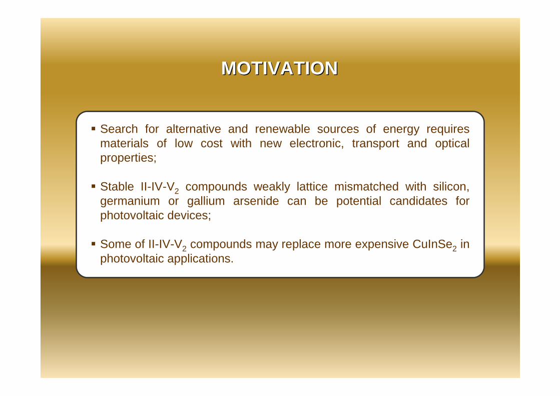
Search for alternative and renewable sources of energy requires materials of low cost with new electronic, transport and opticalproperties;
Stable II-IV-V2 compounds weakly lattice mismatched with silicon, germanium or gallium arsenide can be potential candidates for photovoltaic devices;
Some of II-IV-V2 compounds may replace more expensive CuInSe2 in photovoltaic applications.
MOTIVATIONMOTIVATION
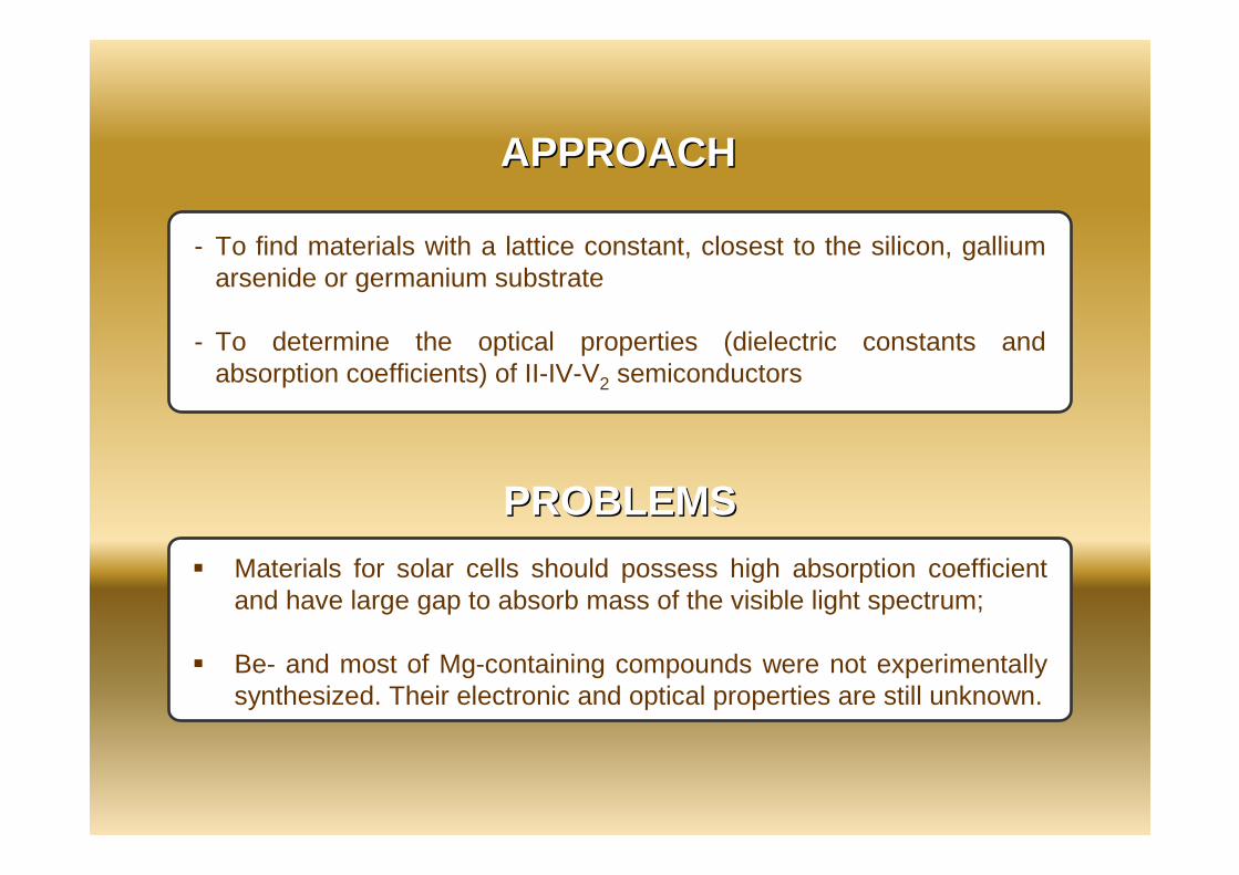
- To find materials with a lattice constant, closest to the silicon, gallium arsenide or germanium substrate
- To determine the optical properties (dielectric constants and absorption coefficients) of II-IV-V2 semiconductors
APPROACHAPPROACH
PROBLEMSPROBLEMS
Materials for solar cells should possess high absorption coefficient and have large gap to absorb mass of the visible light spectrum;
Be- and most of Mg-containing compounds were not experimentally synthesized. Their electronic and optical properties are still unknown.
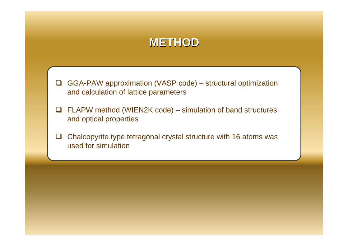
GGA-PAW approximation (VASP code) – structural optimization and calculation of lattice parameters
FLAPW method (WIEN2K code) – simulation of band structures and optical properties
Chalcopyrite type tetragonal crystal structure with 16 atoms wasused for simulation
METHODMETHOD
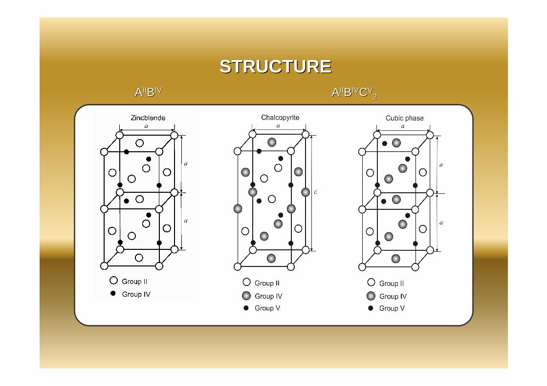
STRUCTURESTRUCTUREAAIIIIBBIVIV AAIIIIBBIVIVCCVV
22
STRUCTURESTRUCTURE
Si Ge Sn5.0
5.2
5.4
5.6
5.8
6.0
6.2
X
GaA
s
a, A
ng
Si
BeXP2
BeXAs2
MgXP2
MgXAs2
ZnXP2
ZnXAs2
CdXP2
CdXAs2
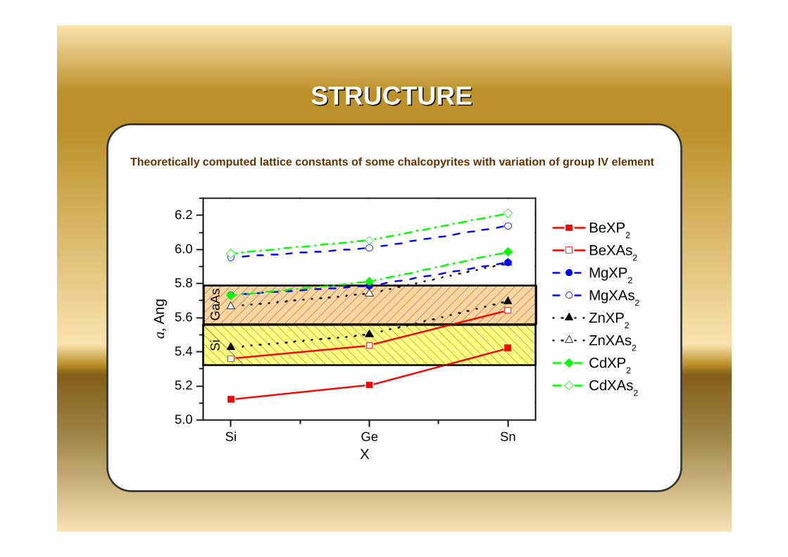
Theoretically computed lattice constants of some ch alcopyrites with variation of group IV element

Be-compounds
-3
-2
-1
0
1
2
3
4
-3
-2
-1
0
1
2
3
4
-3
-2
-1
0
1
2
3
4
-3
-2
-1
0
1
2
3
4
NГ
Ene
rgy,
eV
BeSiAs2
T
N
Г
BeGeAs2
T
N
Г
BeGeP2
T NГ
Ene
rgy,
eV
BeSiP2
T
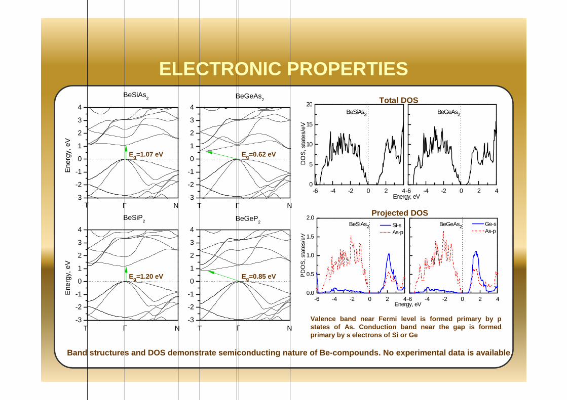
ELECTRONIC PROPERTIES
Eg=1.07 eV Eg=0.62 eV
Eg=1.20 eV Eg=0.85 eV
-6 -4 -2 0 2 4-6 -4 -2 0 2 40.0
0.5
1.0
1.5
2.0
Ge-s As-p
BeGeAs2BeSiAs2
PD
OS
, sta
tes/
eVEnergy, eV
Si-s As-p
Valence band near Fermi level is formed primary by p states of As. Conduction band near the gap is forme d primary by s electrons of Si or Ge
Total DOS
Projected DOS
Band structures and DOS demonstrate semiconducting nature of Be-compounds. No experimental data is ava ilable.
-6 -4 -2 0 2 4-6 -4 -2 0 2 40
5
10
15
20
BeGeAs2
BeSiAs2
DO
S, s
tate
s/eV
Energy, eV
0 2 4 6 8 100
5
10
15
20
25
30
0 2 4 6 8 100
5
10
15
20
25
30
0 2 4 6 8 100
5
10
15
20
25
30
0 2 4 6 8 100
5
10
15
20
25
30
E||x E||z
ε 2
BeSiAs2
E||x E||z
BeGeAs2
E||x E||z
Energy, eV
BeGeP2
E||x E||z
Energy, eV
ε 2
BeSiP2
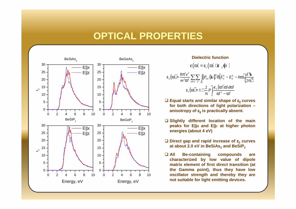
OPTICAL PROPERTIES
Equal starts and similar shape of εεεε2222 curves for both directions of light polarization –anisotropy of εεεε2222 is practically absent.
Slightly different location of the main peaks for E||a and E||c at higher photon energies (about 4 eV)
Direct gap and rapid increase of εεεε2 curves at about 2.0 eV in BeSiAs 2 and BeSiP 2
All Be-containing compounds are characterized by low value of dipole matrix element of first direct transition (at the Gamma point), thus they have low oscillator strength and thereby they are not suitable for light emitting devices.
( ) ( ) ( )( )3
32
22
22
22
8
πω−−δ
ωπ=ωε ′
′≠ ′ Ω′∑∑∫
kk
dEEP
m
e kn
kn
nn nnn h
Dielectric function
( ) ( ) ( )1 2iε ω = ε ω + ε ω
( ) ( )∫∞
ω−ω′ω′ω′ω′ε
π+=ωε
022
21
21
dP
OPTICAL PROPERTIES
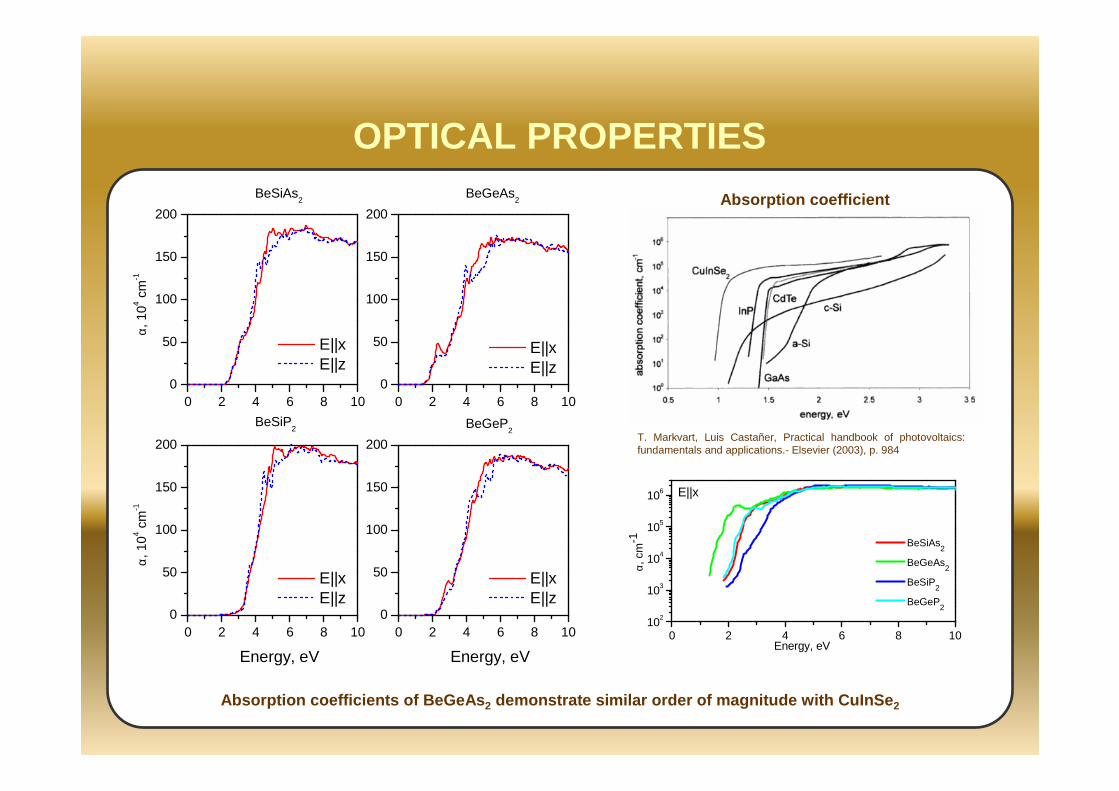
T. Markvart, Luis Castañer, Practical handbook of photovoltaics: fundamentals and applications.- Elsevier (2003), p. 984
Absorption coefficient
0 2 4 6 8 100
50
100
150
200
0 2 4 6 8 100
50
100
150
200
0 2 4 6 8 100
50
100
150
200
0 2 4 6 8 100
50
100
150
200
E||x E||z
α, 1
04 cm
-1
BeSiAs2
E||x E||z
BeGeAs2
E||x E||z
Energy, eV
BeGeP2
E||x E||z
Energy, eV
α, 1
04 cm
-1
BeSiP2
Absorption coefficients of BeGeAs 2 demonstrate similar order of magnitude with CuInSe 2
0 2 4 6 8 10102
103
104
105
106 E||x
BeSiAs2
BeGeAs2
BeSiP2
BeGeP2
α, c
m-1
Energy, eV
Mg-compounds
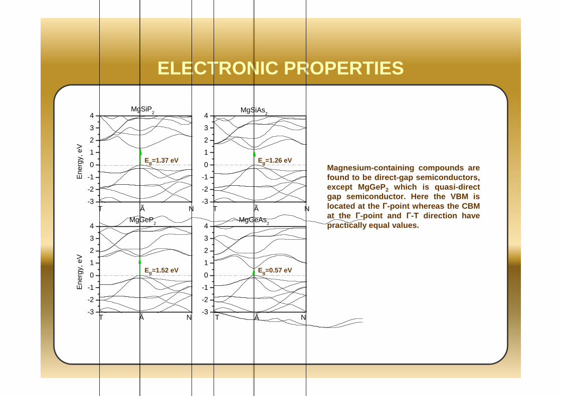
ELECTRONIC PROPERTIES
-3
-2
-1
0
1
2
3
4
-3
-2
-1
0
1
2
3
4
-3
-2
-1
0
1
2
3
4
-3
-2
-1
0
1
2
3
4
NÃ
Ene
rgy,
eV
MgSiP2
T
N
Ã
MgSiAs
2
T
N
Ã
MgGeAs2
T NÃ
Ene
rgy,
eV
MgGeP2
T
Eg=1.37 eV Eg=1.26 eV
Eg=1.52 eV Eg=0.57 eV
Magnesium-containing compounds are found to be direct-gap semiconductors, except MgGeP 2 which is quasi-direct gap semiconductor. Here the VBM is located at the Γ-point whereas the CBM at the Γ-point and Γ-T direction have practically equal values.
OPTICAL PROPERTIES
0 2 4 6 8 100
5
10
15
20
25
30
0 2 4 6 8 100
5
10
15
20
25
30
0 2 4 6 8 100
5
10
15
20
25
30
0 2 4 6 8 100
5
10
15
20
25
30
E||x E||z
ε 2
MgSiP2
Energy, eV Energy, eV
E||x E||z
MgGeAs2
E||x E||z
MgGeP2
E||x E||z
ε 2
MgSiAs2
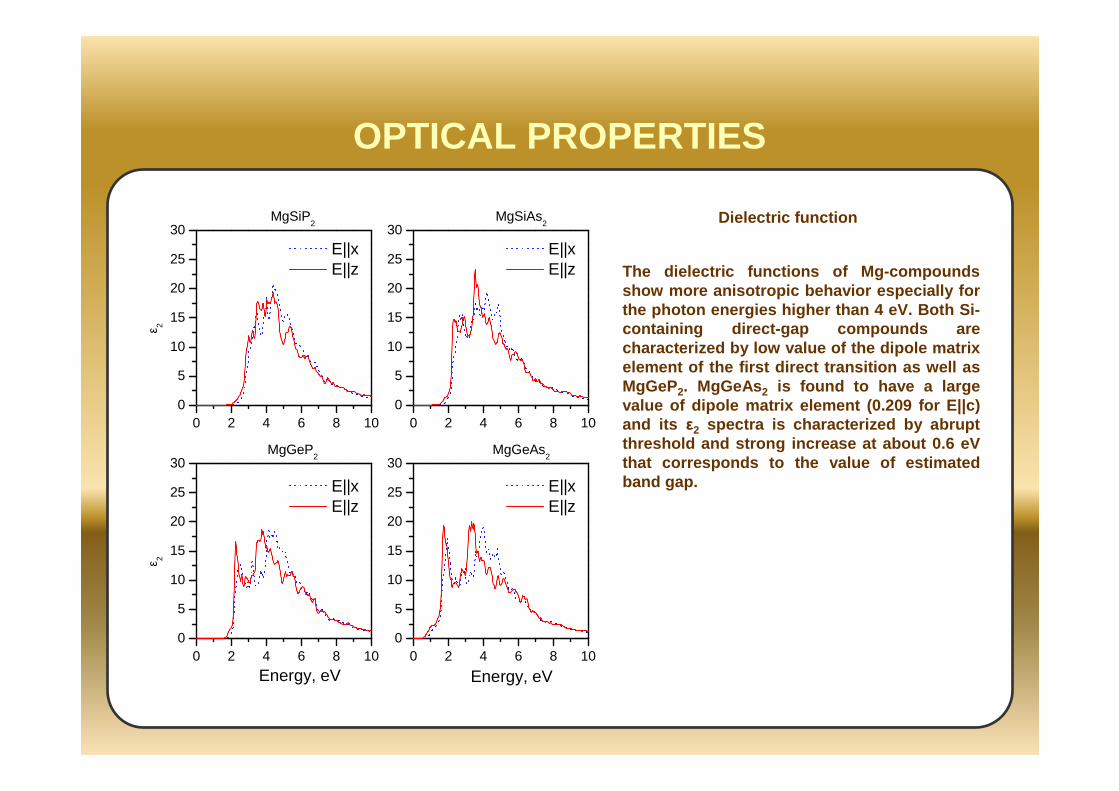
The dielectric functions of Mg-compounds show more anisotropic behavior especially for the photon energies higher than 4 eV. Both Si-containing direct-gap compounds are characterized by low value of the dipole matrix element of the first direct transition as well as MgGeP2. MgGeAs 2 is found to have a large value of dipole matrix element (0.209 for E||c) and its ε2 spectra is characterized by abrupt threshold and strong increase at about 0.6 eV that corresponds to the value of estimated band gap.
Dielectric function
OPTICAL PROPERTIES
0 2 4 6 8 100
50
100
150
200
0 2 4 6 8 100
50
100
150
200
0 2 4 6 8 100
50
100
150
200
0 2 4 6 8 100
50
100
150
200
Energy, eV
E||x E||z
α, 1
04 cm
-1
MgSiAs2
Energy, eV
E||x E||z
MgGeAs2
E||x E||z
MgGeP2
E||x E||z
α, 1
04 cm
-1
MgSiP2 Absorption coefficient
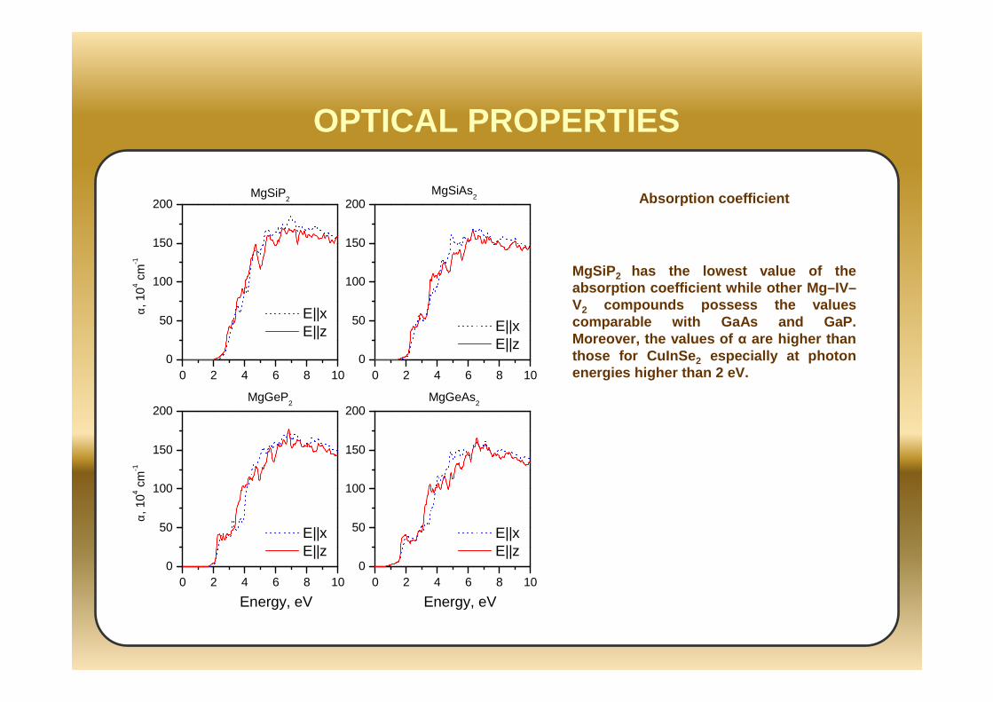
MgSiP 2 has the lowest value of the absorption coefficient while other Mg–IV–V2 compounds possess the values comparable with GaAs and GaP. Moreover, the values of α are higher than those for CuInSe 2 especially at photon energies higher than 2 eV.
Zn-compounds
ELECTRONIC PROPERTIES
-3
-2
-1
0
1
2
3
4
-3
-2
-1
0
1
2
3
4
-3
-2
-1
0
1
2
3
4
-3
-2
-1
0
1
2
3
4
NГ
Ene
rgy,
eV
ZnSiAs2
T
N
Г
ZnGeAs2
T
N
Г
ZnGeP2
T NГ
Ene
rgy,
eV
ZnSiP2
T
10 20 30 40 50
0.00.40.81.21.62.02.4
Eg,
eV
atomic number
calc. ref.
ZnGeP-As-Sb2
P As Sb
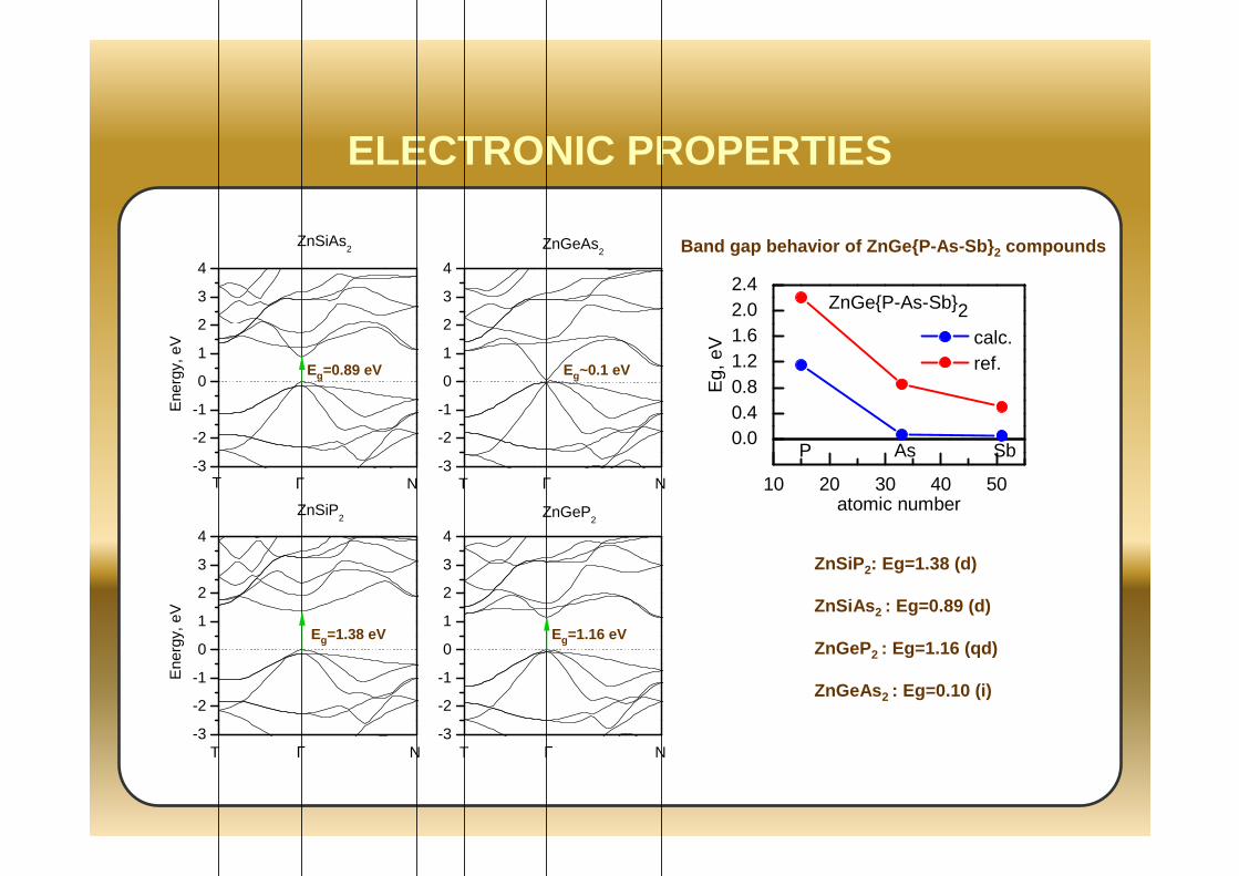
Band gap behavior of ZnGeP-As-Sb 2 compounds
ZnSiP 2: Eg=1.38 (d)
ZnSiAs 2 : Eg=0.89 (d)
ZnGeP2 : Eg=1.16 (qd)
ZnGeAs 2 : Eg=0.10 (i)
Eg=0.89 eV
Eg=1.38 eV Eg=1.16 eV
Eg~0.1 eV
0 2 4 6 8 100
5
10
15
20
25
30
0 2 4 6 8 100
5
10
15
20
25
30
0 2 4 6 8 100
5
10
15
20
25
30
0 2 4 6 8 100
5
10
15
20
25
30
E||x E||z
ε 2
ZnSiAs2
E||x E||z
ZnGeAs2
E||x E||z
Energy, eV
ZnGeP2
E||x E||z
Energy, eV
ε 2
ZnSiP2
OPTICAL PROPERTIES
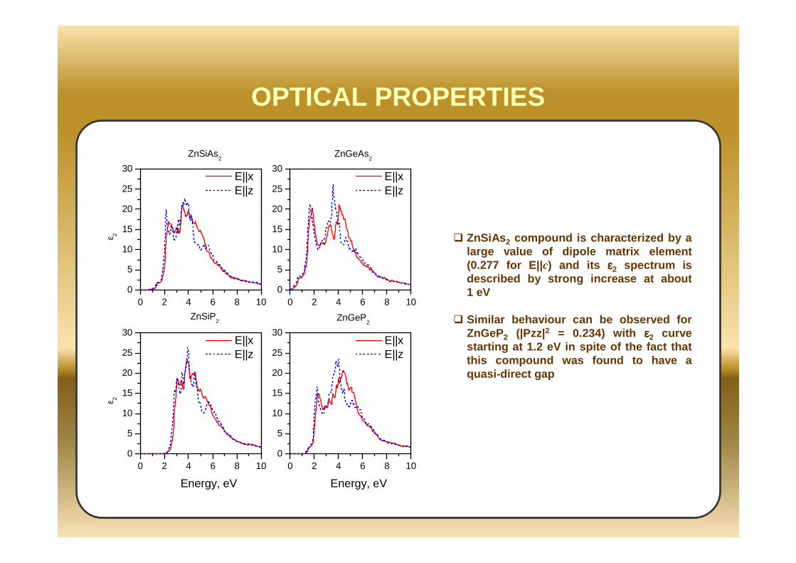
ZnSiAs 2 compound is characterized by a large value of dipole matrix element (0.277 for E||c) and its εεεε2 spectrum is described by strong increase at about 1 eV
Similar behaviour can be observed for ZnGeP2 (|Pzz|2 = 0.234) with εεεε2 curve starting at 1.2 eV in spite of the fact that this compound was found to have a quasi-direct gap
0 2 4 6 8 100
50
100
150
200
0 2 4 6 8 100
50
100
150
200
0 2 4 6 8 100
50
100
150
200
0 2 4 6 8 100
50
100
150
200
E||x E||z
α, 1
04 cm
-1
ZnSiAs2
E||x E||z
ZnGeAs2
E||x E||z
Energy, eV
ZnGeP2
E||x E||z
Energy, eV
α, 1
04 cm
-1
ZnSiP2
OPTICAL PROPERTIES
T. Markvart, Luis Castañer, Practical handbook of photovoltaics: fundamentals and applications.- Elsevier (2003), p. 984
Absorption coefficient
0 2 4 6 8 10
104
105
106 E||x
Energy, eV
ZnSiAs2
ZnGeAs2
ZnSiP2
ZnGeP2
α, c
m-1
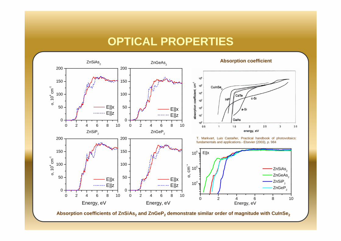
Absorption coefficients of ZnSiAs 2 and ZnGeP 2 demonstrate similar order of magnitude with CuInSe 2
Cd-compounds
-3
-2
-1
0
1
2
3
4
-3
-2
-1
0
1
2
3
4
-3
-2
-1
0
1
2
3
4
-3
-2
-1
0
1
2
3
4
NГ
Ene
rgy,
eV
CdSiAs2
T
N
Г
CdGeAs2
T
N
Г
CdGeP2
T NГ
Ene
rgy,
eV
CdSiP2
T
ELECTRONIC PROPERTIES
10 20 30 40 50
0.0
0.4
0.8
1.2
1.6
Eg,
eV
atomic number
calc.
ref.
CdGeP-As-Sb2
P As Sb
Band gap behaviour of CdGeP-As-Sb 2 compounds
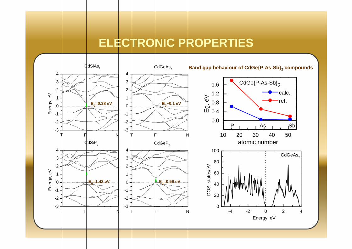
Eg=0.38 eV
Eg=1.42 eV Eg=0.59 eV
Eg~0.1 eV
-4 -2 0 2 40
20
40
60
80
100
DO
S, s
tate
s/eV
Energy, eV
CdGeAs2
0 2 4 6 8 100
5
10
15
20
25
30
0 2 4 6 8 100
5
10
15
20
25
30
0 2 4 6 8 100
5
10
15
20
25
30
0 2 4 6 8 100
5
10
15
20
25
30
E||x E||z
ε 2
CdSiAs2
E||x E||z
CdGeAs2
E||x E||z
Energy, eV
CdGeP2
E||x E||z
Energy, eV
ε 2
CdSiP2
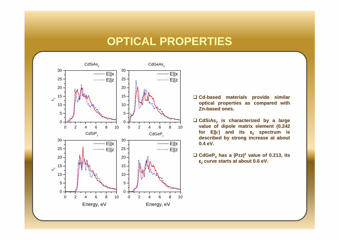
OPTICAL PROPERTIES
Cd-based materials provide similar optical properties as compared with Zn-based ones.
CdSiAs 2 is characterized by a large value of dipole matrix element (0.242 for E||c) and its εεεε2 spectrum is described by strong increase at about 0.4 eV.
CdGeP2 has a |Pzz| 2 value of 0.213, its εεεε2 curve starts at about 0.6 eV.
0 2 4 6 8 100
50
100
150
200
0 2 4 6 8 100
50
100
150
200
0 2 4 6 8 100
50
100
150
200
0 2 4 6 8 100
50
100
150
200
E||x E||z
α, 1
04 cm
-1
CdSiAs2
E||x E||z
CdGeAs2
E||x E||z
Energy, eV
CdGeP2
E||x E||z
Energy, eV
α, 1
04 cm
-1
CdSiP2
OPTICAL PROPERTIES
T. Markvart, Luis Castañer, Practical handbook of photovoltaics: fundamentals and applications.- Elsevier (2003), p. 984
Absorption coefficient
0 2 4 6 8 10101
102
103
104
105
106 E||x
Energy, eV
CdSiAs2
CdGeAs2
CdSiP2
CdGeP2
α, 1
04 cm
-1
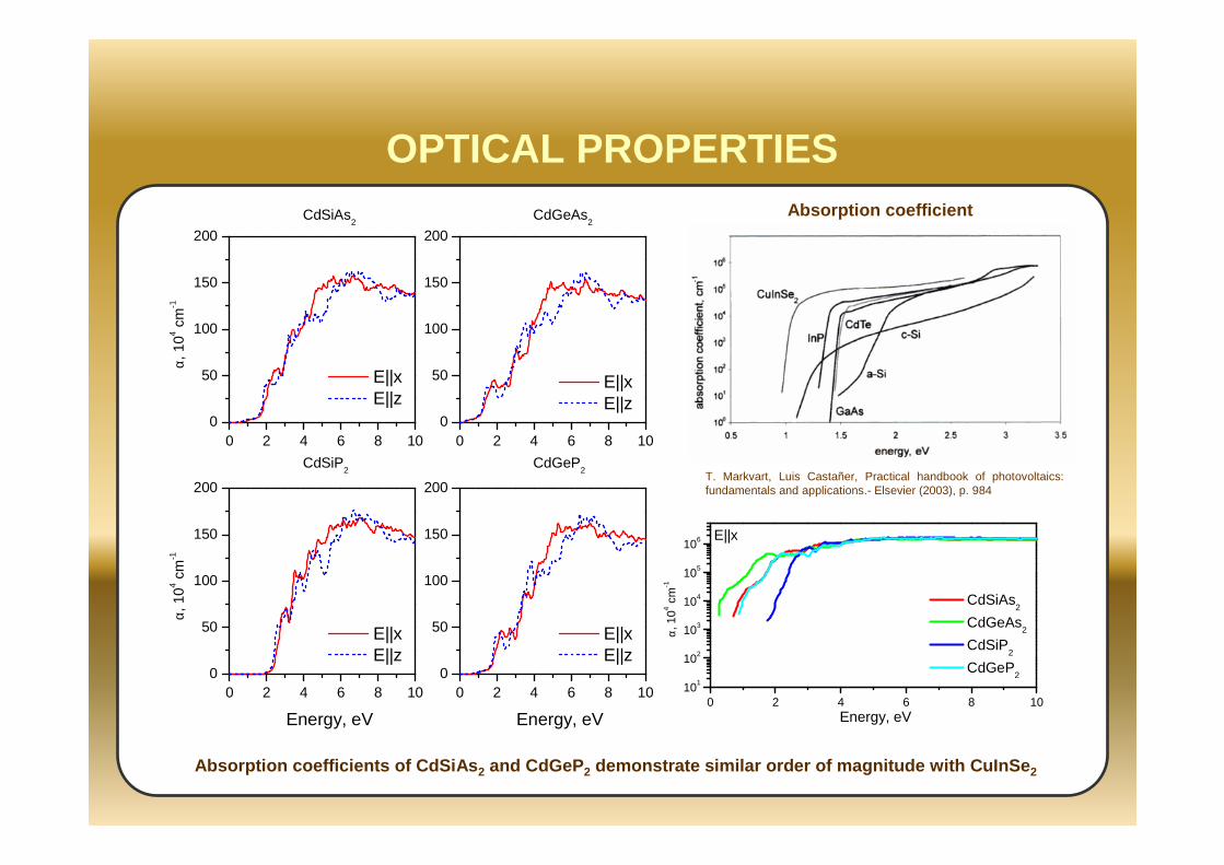
Absorption coefficients of CdSiAs 2 and CdGeP 2 demonstrate similar order of magnitude with CuInSe 2
GENERAL REMARKSGENERAL REMARKS
One of the possible ways to increase the quantum efficiency of solar cell is multilayered heterostructures consisting of semiconducting materials with different band gaps.
For photovoltaic applications we are interested in stable compounds having a direct gap (absorption coefficients and effective masses are higher for direct gaps as compared to indirect ones).
If we want eliminate expensive, rare, dangerous or too toxic elements it is better do not consider Cd-based and P containing compounds, as phosphorous is highly volatile, red-phosphorous burns, and phosphinegas is highly toxic.
Among materials of II-IV-V2 class arsenic compounds are easier to be obtained experimentally in comparison with nitrogen and phosphorous based ternaries.
Zn(Si, Sn)As2 family should possess lattice constants close to GaAs one and have band gap suitable for photovoltaics.
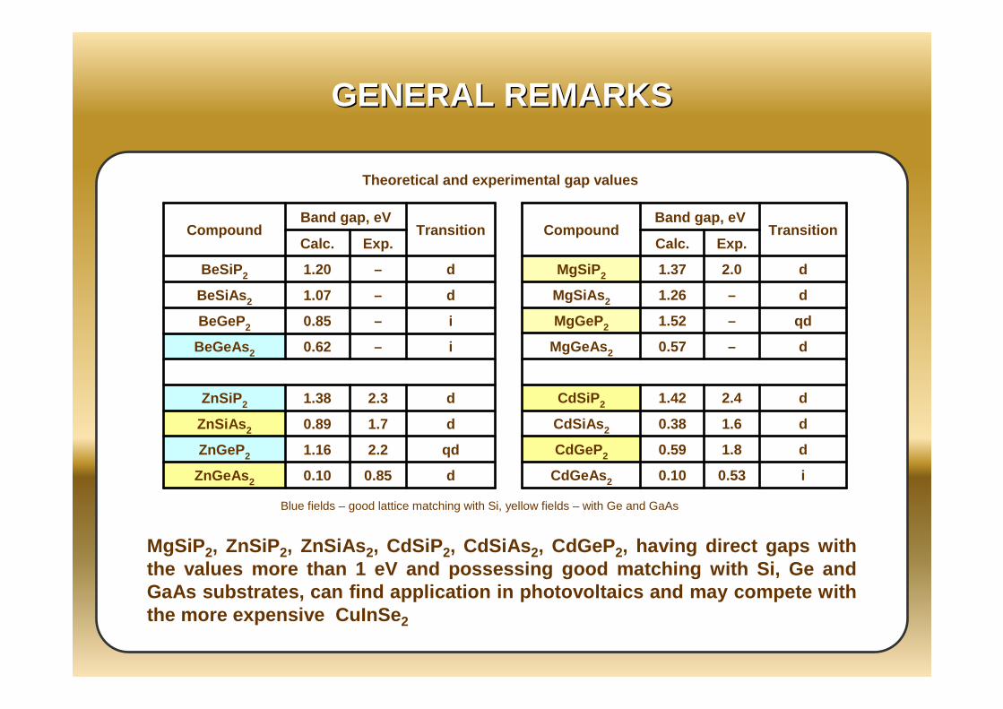
MgSiP2, ZnSiP2, ZnSiAs 2, CdSiP2, CdSiAs 2, CdGeP2, having direct gaps with the values more than 1 eV and possessing good match ing with Si, Ge and GaAs substrates, can find application in photovoltai cs and may compete with the more expensive CuInSe 2
d0.850.10ZnGeAs 2
qd2.21.16ZnGeP2
d1.70.89ZnSiAs 2
d2.31.38ZnSiP 2
i–0.62BeGeAs 2
i–0.85BeGeP2
d–1.07BeSiAs 2
d–1.20BeSiP 2
Exp.Calc.Transition
Band gap, eVCompound
Theoretical and experimental gap values
Blue fields – good lattice matching with Si, yellow fields – with Ge and GaAs
i0.530.10CdGeAs 2
d1.80.59CdGeP2
d1.60.38CdSiAs 2
d2.41.42CdSiP 2
d–0.57MgGeAs 2
qd–1.52MgGeP2
d–1.26MgSiAs 2
d2.01.37MgSiP 2
Exp.Calc.Transition
Band gap, eVCompound
GENERAL REMARKSGENERAL REMARKS
GENERAL REMARKSGENERAL REMARKS
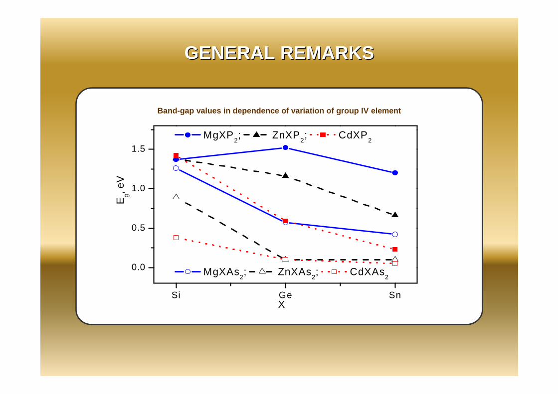
Si Ge Sn
0.0
0.5
1.0
1.5
X
Eg, e
V
MgXAs2; ZnXAs
2; CdXAs
2
MgXP2; ZnXP
2; CdXP
2
Band-gap values in dependence of variation of group IV element
1.0 1.5 2.0 2.5 3.0 3.50.2
0.3
0.4
0.5
R
Photon energy, eV
MgSnAs2
ZnSnAs2
ZnSiAs2
CdGeAs2
CdSiAs2
CuInSe2
GaAs GaP
1200
1000
800
600
400
λ, nm
1.0 1.5 2.0 2.5 3.0 3.5
2
4
6
8
10
1200
1000
800
600
400
α, 1
05 cm
-1
Photon energy, eV
λ, nm
Averaged absorption coefficients of II–IV–V 2 ternaries in comparison with GaAs, GaP and CuInSe 2
Averaged reflectance spectra of II–IV–V 2 ternaries in comparison with GaAs, GaP and CuInSe 2
GENERAL REMARKSGENERAL REMARKS
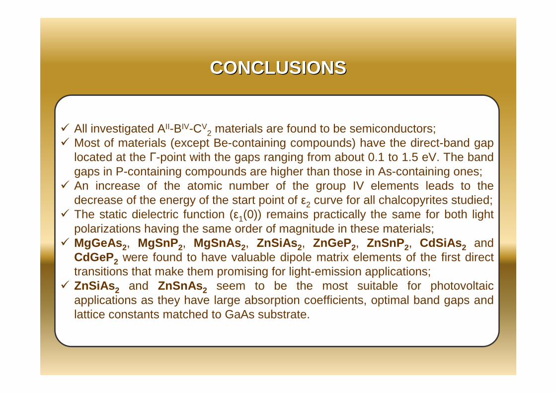
All investigated AII-BIV-CV2 materials are found to be semiconductors;
Most of materials (except Be-containing compounds) have the direct-band gap located at the Γ-point with the gaps ranging from about 0.1 to 1.5 eV. The band gaps in P-containing compounds are higher than those in As-containing ones;
An increase of the atomic number of the group IV elements leads to the decrease of the energy of the start point of ε2 curve for all chalcopyrites studied;
The static dielectric function (ε1(0)) remains practically the same for both light polarizations having the same order of magnitude in these materials;
MgGeAs 2, MgSnP2, MgSnAs 2, ZnSiAs 2, ZnGeP2, ZnSnP2, CdSiAs 2 and CdGeP2 were found to have valuable dipole matrix elements of the first direct transitions that make them promising for light-emission applications;
ZnSiAs 2 and ZnSnAs 2 seem to be the most suitable for photovoltaic applications as they have large absorption coefficients, optimal band gaps and lattice constants matched to GaAs substrate.
CONCLUSIONSCONCLUSIONS

Thank you for your Thank you for your attention!attention!


![Finale 2003 - [Marcha Nupcial de Mendelssohn.MUS]rede.cultura.ce.gov.br/banco-de-partituras/wp-content/...bb # # # # # # # bb bb bb bb Flauta (C) Requinta (Eb) 1º Clarinete (Bb) 2º](https://static.fdocuments.ec/doc/165x107/6103dbb13f2bd2361879278f/finale-2003-marcha-nupcial-de-redeculturacegovbrbanco-de-partituraswp-content.jpg)


![Finale 2002b - [partitura buena.MUS]pop-sheet-music.com/.../3bf3c3cf7a06cee73c5106ab04ad5a66.pdf · 2015-02-23 · v & & &??? Ö Ö & Ö bb bb # # # # bb bb bb 4 2 4 2 4 2 4 2 42](https://static.fdocuments.ec/doc/165x107/5e29b8db29f99e4d883529f9/finale-2002b-partitura-buenamuspop-sheet-musiccom3bf3c3cf7a06-2015-02-23.jpg)