0 37 S/0.37 mS/ μm I In0.53 GGa0.47 A MOSFET ith …...0 37 S/0.37 mS/μm I In0.53GGa0.47A MOSFET...
18
0 37 S/ I G A MOSFET ith 5 h l d 0.37 mS/μm In 0.53 Ga 0.47 As MOSFET with 5 nm channel and self-aligned epitaxial raised source/drain Uttam Singisetti*, Mark A. Wistey, Greg J. Burek, Ashish K. Baraskar, Joel Cagnon, B. J. Thibeault, S. Stemmer , A.C. Gossard, and M.J.W. Rodwell ECE and Materials Departments University of California, Santa Barbara, CA Eun Ji Kim, Byungha Shin, and Paul C McIntyre Materials Science and Engineering, Stanford University, Stanford, CA Yong-ju Lee Intel Corporation, Santa Clara, CA 2009 Device Research Conference DRC 2009 1 2009 Device Research Conference Pennsylvania State University, State College, PA *[email protected]
Transcript of 0 37 S/0.37 mS/ μm I In0.53 GGa0.47 A MOSFET ith …...0 37 S/0.37 mS/μm I In0.53GGa0.47A MOSFET...

0 37 S/ I G A MOSFET ith 5 h l d 0.37 mS/μm In0.53Ga0.47As MOSFET with 5 nm channel and self-aligned epitaxial raised source/drain
Uttam Singisetti*, Mark A. Wistey, Greg J. Burek, Ashish K. Baraskar, Joel Cagnon, B. J. Thibeault, S. Stemmer, A.C. Gossard, and M.J.W. Rodwell, , ,
ECE and Materials DepartmentsUniversity of California, Santa Barbara, CA
Eun Ji Kim, Byungha Shin, and Paul C McIntyreMaterials Science and Engineering, Stanford University, Stanford, CA
Yong-ju LeeIntel Corporation, Santa Clara, CA
2009 Device Research Conference
DRC 20091
2009 Device Research ConferencePennsylvania State University, State College, PA
Outline
• Motivation: III-V MOSFETs
• Approach: Self-aligned source/drain by MBE regrowthpp g y g
• FET and contacts Results
• Conclusion and future work
DRC 20092

Why III-V MOSFETs
Silicon MOSFETs:Gate oxide may limit <16 nm scaling Gate oxide may limit <16 nm scaling
IBM 45nm NMOSNarayan et al, VLSI 2006
Id / Wg ~ cox(Vg-Vth)vinj
Id / Qtransit ~ vinj / Lg
Alternative: In0.53Ga0.47As channel MOSFETs0.53 0.47
low m* (0.041 mo) → high injection velocity (~ 2×107 cm/s)*
→ increase drive current, decreased CV/I
DRC 20093
* Enoki et al , EDL 1990
increase drive current, decreased CV/I

Target device structure
0
1
2
3
y (e
V)
Al2O
3
-3
-2
-1
0
Ener
gy
InGaAs InAlAs
Target 22 nm gate length-4
0 50 100 150 200 250Y (Ang.)
Control of short-channel effects vertical scaling1 nm EOT: thin gate dielectric, surface-channel device5 nm quantum well thicknessq<5 nm deep source / drain regions
~3 mA/μm target drive current low access resistanceself aligned low resisitivity source / drain contacts
DRC 20094
self-aligned, low resisitivity source / drain contactsself-aligned N+ source / drain regions with high doping

22 nm InGaAs MOSFET: source resistance
LgLS/D
i
did Rg
II⋅+
=1 g
DSsheet
DSg
cs W
LLW
R2
/
/
ρρ+=
IBM High-k Metal gate transistorImage Source:EE Times
smi Rg+1 gDSg /
• Source access resistance degrades Id and gmg d gm
• IC Package density : LS/D ~ Lg =22 nm ρc must be low• Need low sheet resistance in thin ~5 nm N+ layer
DRC 20095
y• Design targets: ρc ~1 Ω−μm2, ρsheet ~ 400 Ω

22nm ion implanted InGaAs MOSFET
Key Technological Challenges
• Shallow junctions ( ~ 5 nm), high (~5×1019 cm-3) doping • Doping abruptness ( ~ 1 nm/decade)• Doping abruptness ( 1 nm/decade)• Lateral Straggle ( ~ 5 nm)• Deep junctions would lead to degraded short channel effects
DRC 20096
• Deep junctions would lead to degraded short channel effects

InGaAs MOSFET with raised source/drain by regrowth
HAADF-STEM1*
InGaAsregrowth
Interface
InGaAs
regrowth
2 nm
InGaAs
* TEM by J. Cagnon, Susanne Stemmer Group, UCSB
Self-aligned source/drain defined by MBE regrowth1
Self aligned in situ Mo contacts2Self-aligned in-situ Mo contacts2
Process flow & dimensions selected for 22 nm Lg design;present devices @ 200 nm gate length
DRC 20097
1Wistey, EMC 20082Baraskar, EMC 2009
present devices @ 200 nm gate length

Regrown S/D process: key features
Self-aligned & low resistivityg y...source / drain N+ regions...source / drain metal contacts
Vertical S/D doping profile set by MBEabrupt on ~ 1 nm scale
Gate-firstgate dielectric formed after MBE growth
DRC 20098
uncontaminated / undamaged surface

Process flow*
DRC 20099* Singisetti et al; Physica Status Solidi C, vol. 6, pp. 1394,2009
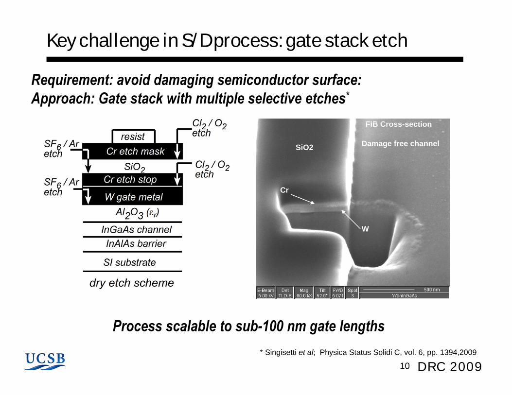
Key challenge in S/D process: gate stack etch
FIB Cross section
Requirement: avoid damaging semiconductor surface:Approach: Gate stack with multiple selective etches*
SiO2
FIB Cross-section
Damage free channel
Cr
W
P l bl t b 100 t l th
DRC 200910
Process scalable to sub-100 nm gate lengths* Singisetti et al; Physica Status Solidi C, vol. 6, pp. 1394,2009

Key challenge in S/D process: dielectric sidewall
Sidewall must be kept thin: avoid carrier depletion, source starvation.
• Target < 15 nm sidewall in 22 nm Lg device Target 15 nm sidewall in 22 nm Lg device • 20-25 nm SiNx thick sidewalls in present devices• Pulse doping in the barrier: compensate for carrier depletion from Dit
DRC 200911
Pulse doping in the barrier: compensate for carrier depletion from Dit

MOSFET SEMs
SiO2SiO2
WCr
InGaAsregrowth
SiNx
WCr
InGaAsregrowth
SiNx
W
Originalinterface
W
Originalinterface Ti/Au Pad
Mo+InGaAs
Ti/Au Pad
Mo+InGaAs
Cross-section after regrowth, b t b f M d iti
Top view of completed devicebut before Mo deposition
DRC 200912

MOSFET characteristics
4 7 Al 0 1×10¹³ 2 l d i
0.8
1L
g=0.8μm, W
g,eff=9μm
Vgs
= -1 V to 3.5, Vgs step
=0.5 V
4.7 nm Al203 , 1×1013 cm-2 pulse doping
0.8
1L
g=1.0μm, W
g,eff=12μm
Vgs
= -1 V to 3.5, Vgs step
=0.5 V
0.4
0.6
gs gs_step
I ds(m
A/μ
m)
0.4
0.6
ds(m
A/μ
m)
gs gs_step
0
0.2
0 0 5 1 1 5 20
0.2
0 0 5 1 1 5 2
I d
0 0.5 1 1.5 2V
ds(V)
• Maximum Drive current (Id): 0.95 mA/μm
0 0.5 1 1.5 2V
ds(V)
• Peak transconductance (gm): 0.37 mS/μm
DRC 200913
Id and gm below expected values

FET source resistance
7000 SEM
5000
6000
7000V
gs=3.0 V
m)
2000
3000
4000R
on (Ω
−μm
InGaAs regrowth on unprocessed thin InP*0
1000
0 2 4 6 8 10Gate Length (μm)
RS+R
D
= 1.0 kΩ−μm
• Series resistance estimated by extrapolating Ron to zero gate length
g (μ )
• Source access resistance ~ 500 Ω−μm
DRC 200914

Source resistance : regrowth TLMs
W / Cr / SiO2 gate
SEM
N th
SEMInGaAs regrowth
FETRegrowth TLMs25
30
35
40
ce (Ω
)
W~ 20 μm
2 g No regrowth
10
15
20
Res
ista
nc
Rsh
~ 29 Ω
0
5
0 5 10 15 20 25 30Contact Separation ( μm)
Rc ~ 5.5 Ω−μm2 (12.6 Ω−μm)
• TLMs fabricated on the regrowth far away from the gate
• Regrowth sheet resistance ~ 29 Ωg
• Mo/InGaAs contact resistance ~ 5.5 Ω−μm2 (12.6 Ω−μm)
DRC 200915
TLM data does not explain 500 Ω−μm observed FET source resistance

Source resistance: electron depletion near gate
SiOSiOSiO2
InGaAsregrowth
SiNx
SiO2
InGaAsregrowth
SiNx
WCr
Originalinterface
g
WCr
Originalinterface
g
R1 interfaceinterfaceR1
R2
• Electron depletion in regrowth shadow region (R1 )1
• Electron depletion in the channel under SiNx sidewalls (R2 )
DRC 200916

InAs source/drain regrowth
InAsregrowthGate regrowth
side of gate
top of gate
M S/D t l ith Mo S/D metal with N+ InAs underneath
Improved InAs regrowth with low As flux for uniform filling1Improved InAs regrowth with low As flux for uniform filling
InAs less susceptible to electron depletion: Fermi pinning above Ec2
DRC 200917
1 Wistey et al, EMC 2009 Wistey et al NAMBE 2009.
2Bhargava et al , APL 1997

Conclusion
• Self-aligned raised source/drain for scaled channel ( 5nm)
• D-FETs: peak Id = 0.95 mA/μm, and peak gm =0.37 mS/μm
• InAs Source/Drain E-FETs1
• Next: Next: scale to ~50 nm Lggate dielectric quality
S C
DRC 200918
This work was supported by Semiconductor Research Corporation under theNon-classical CMOS Research Program
1Singisetti et al, EDL submitted